

Page 1
CS5521/22/23/24/28
16-bit or 24-bit, 2/4/8-channel ADCs with PGIA
Features
z Low Input Current (100 pA), Chopper-
stabilized Instrumentation Amplifier
z Scalable Input Span (Bipolar/Unipolar)
- 2.5V VREF: 25 mV, 55 mV, 100 mV, 1 V,
2.5V, 5V
- External: 10 V, 100 V
z Wide V
z Fourth Order Delta-Sigma A/D Converter
z Easy to Use Three-wire Serial Interface Port
- Programmable/Auto Channel Sequencer with
Conversion Data FIFO
- Accessible Calibration Registers per Channel
- Compatible with SPI™
z System and Self Calibration
z Eight Selectable Word Rates
- Up to 617 Sps (XIN = 200 kHz)
- Single Conversion Settling
- 50/60 Hz ±3 Hz Simultaneous Rejection
z Single +5 V Power Supply Operation
- Charge Pump Drive for Negative Supply
- +3 to +5 V Digital Supply Operation
z Low Power Consumption: 6.0 mW
Input Range (+1 to +5 V)
REF
and Microwire
General Description
The CS5521/22/23/24/28 are highly integrated ∆Σ analog-to-digital converters (ADCs) which use chargebalance techniques to achieve 16-bit (CS5521/23) and
24-bit (CS5522/24/28) performance. The ADCs
either two-channel (CS5521/22), four-channel
(CS5523/24), or eight-channel (CS5528) devices and
include a low-input-current, chopper-stabilized instrumentation amplifier. To permit selectable input spans of
25 mV, 55 mV, 100 mV, 1 V, 2.5 V, and 5 V, the ADCs
include a PGA (programmable gain amplifier). To accommodate ground-based thermocouple applications,
the devices include a charge pump drive which provides
a negative bias voltage to the on-chip amplifiers.
These devices also include a fourth-order ∆Σ modulator
followed by a digital filter
output word rates
. The digital filters are designed to settle
which provides eight selectable
to full accuracy within one conversion cycle and when
operated at word rates below 30 Sps, they reject both
50 Hz and 60 Hz interference.
These single-supply products are ideal solutions for
measuring isolated and non-isolated, low-level signals in
process control applications.
ORDERING INFORMATION
See page 52.
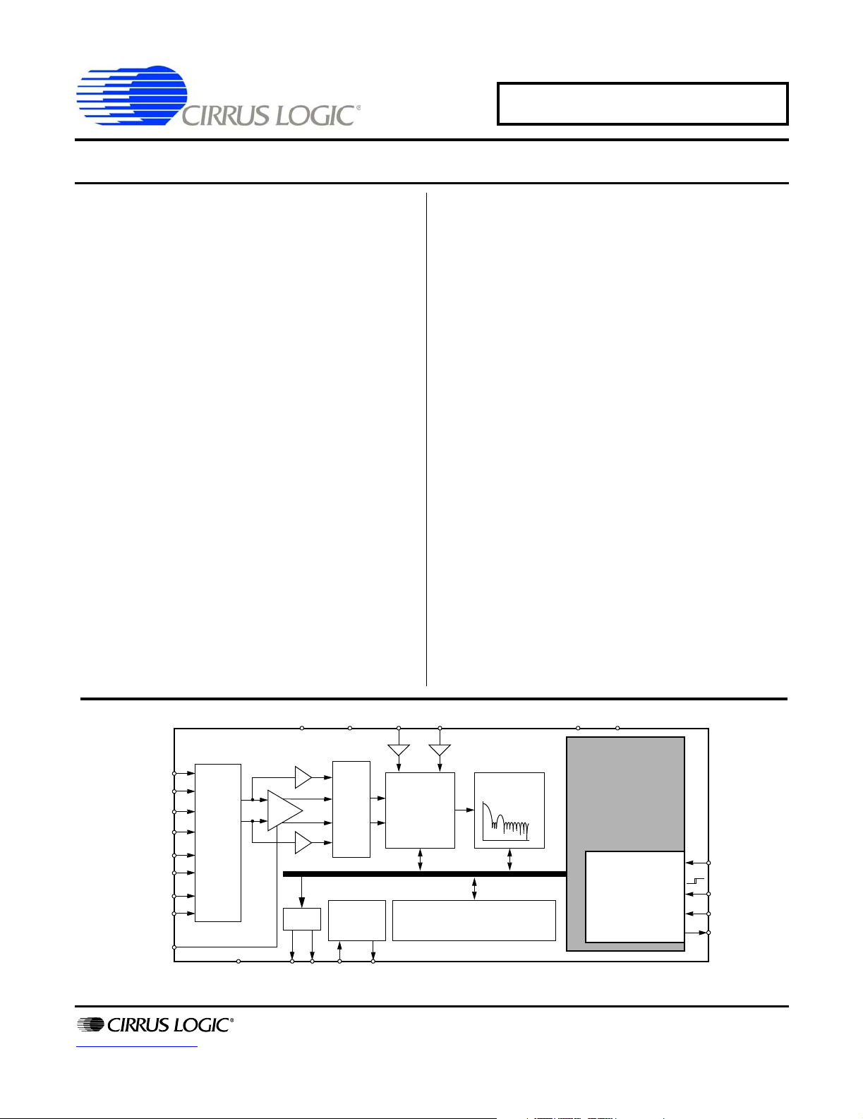
come as
AIN1+
AIN1-
AIN2+
AIN2-
AIN3+
AIN3-
AIN4+
AIN4-
NBV
http://www.cirrus.com
MUX
CS5524
Shown
VA+ AGND VREF+ VREF- VD+DGND
X1
Differential
4th Order
∆Σ
Modulator
Data FIFO &
Calibration R eg ist er s
(All Rights Reserved)
Digital Filter
+
X20
Latch
A0 A1CPD
X1
Gain
X1
Programmable
Clock
Gen.
XIN XOUT
Copyright © Cirrus Logic, Inc. 2005
Controller,
Setup Registers,
&
Channel Scan
Logic
Serial Port
Interface
CS
SCLK
SDI
SDO
AUG ‘05
DS317F4
Page 2

TABLE OF CONTENTS
o
r
d
e
s
s
s
d
R
N
S
E
D
A
M
Y
o
1. CHARACTERISTICS AND SPECIFICATIONS ........................................................................ 5
ANALOG CHARACTERISTICS................................................................................................5
TYPICAL RMS NOISE, CS5521/23.......................................................................................... 7
TYPICAL NOISE FREE RESOLUTION (BITS), CS5521/23 .................................................... 7
TYPICAL RMS NOISE, CS5522/24/28..................................................................................... 8
TYPICAL NOISE FREE RESOLUTION (BITS), CS5522/24/28 ............................................... 8
5 V DIGITAL CHARACTERISTICS...........................................................................................9
3 V DIGITAL CHARACTERISTICS...........................................................................................9
DYNAMIC CHARACTERISTICS ............................................................................................ 10
RECOMMENDED OPERATING CONDITIONS .....................................................................10
ABSOLUTE MAXIMUM RATINGS .........................................................................................10
SWITCHING CHARACTERISTICS ........................................................................................ 11
2. GENERAL DESCRIPTION ..................................................................................................... 13
2.1 Analog Input ........ ....................................... ... ....................................... ... .........................13
2.1.1 Instrumentation Amplifier .........................................................................................14
2.1.2 Coarse/Fine Charge Buffers ...................................... ...................................... ... 14
2.1.3 Analog Input Span Considerations ..........................................................................15
2.1.4 Measuring Voltages Higher than 5 V .................................................................. 15
2.1.5 Voltage Reference ........................................................................ ... ...................16
2.2 Overview of ADC Register Structure and Operating Modes ............................................16
2.2.1 System Initialization ................................... ... ... ....................................... ... .........18
2.2.2 Serial Port Initialization Sequence ............................. ... ... ... .... ............................ 18
2.2.3 Command Register Quick Reference ...................................... ... ... .... ...............19
2.2.4 Command Register Descriptions ........................................................................20
2.2.5 Serial Port Interface ...................................... ... ... ....................................... ... ......25
2.2.6 Reading/Writing the Offset, Gain, and Configuration Registers ................. .........26
2.2.7 Reading/Writing the Channel-Setup Registers ...................................................26
2.2.7.1 Latch Outputs ............ .... ... ....................................... ... ......................... 28
2.2.7.2 Channel Select Bits ............................................................................. 28
2.2.7.3 Output Word Rate Selection ...............................................................28
2.2.7.4 Gain Bits ........... ....................................... ... ...................................... ... 28
CS5521/22/23/24/28
Contacting Cirrus Logic Support
For all product questions and inquiries contact a Cirrus Logic Sales Representative.
To find the one nearest to you go to www.cirrus.com
IMPORTANT NOTICE
Cirrus Logic, Inc. and i ts subsidiaries (“Cirrus”) believe that the i nformation contained in this document is accurate and reliable. However, th e information is subject t
change without notice and is provided “AS IS” without warranty of any kind (express or implied). Customers are advised to obtain the latest version of relevant info
mation to verify, before placing orders, that inform ation being relied on is current and complete. All prod ucts are sold subject to the term s and conditions of sale supp lie
at the time of order acknowl edgment, i ncludin g those per taining to warra nty, in demnifica tion, an d limitat ion of l iabili ty. No r esponsibility is assumed by Cirrus for th
use of this information, including use of this inform atio n as the basis for manufacture or sale of any items, or for infringement of patents or other rights of third partie
This document is the property of Cirrus and by furnishing this information, Cirrus grants no license, express or implied under any patents, mask work rights, copyright
trademarks, trade secrets or other intellectual property rights. Cirrus owns the copyrights associated with the information contained herein and gives consent for copie
to be made of the information on l y for use wi t h i n you r or g aniz a ti on wit h res p ect to Cirr u s integrated circuits or ot h er pr od uc t s of Cirrus. This consent does not ext en
to other copying such as copying for general distribution, advertising or promotional purposes, or for creating any work for resale.
CERTAIN APPLICATIONS USING SEMICONDUCTOR PRODUCTS MAY INVOLVE POTENTIAL RISKS OF DEATH, PERSONAL INJURY, OR SEVERE PROPE
TY OR ENVIRONMENTAL DAMAGE (“CRITICAL APPLICATIONS”). CIRRUS PRODUCTS ARE NOT DESIGNED, AUTHORIZED OR WARRANTED FOR USE I
AIRCRAFT SYSTEMS, MILITARY APPLICATIONS, PRODUCTS SURGICALLY IMPLANTED INTO THE BODY, AUTOMOTIVE SAFETY OR SECURITY DEVICE
LIFE SUPPORT PRODUCTS OR OTHER CRITICAL APPLICATIONS. INCLUSION OF CIRRUS PRODUCTS IN SUCH APPLICATIONS IS UNDERSTOOD TO B
FULLY AT THE CUSTOMER'S RISK AND CIRRUS DISCLAIMS AND MAKES NO WARRANTY, EXPRESS, STATUTORY OR IMPLIED, INCLUDING THE IMPLIE
WARRANTIES OF MERCHANTABILITY AND FITNESS FOR PARTICULAR PURPOSE, WITH REGARD TO ANY CIRRUS PRODUCT THAT IS USED IN SUCH
MANNER. IF THE CUSTOMER OR CUSTOMER'S CUSTOMER USES OR PERMITS THE USE OF CIRRUS PRODUCTS IN CRITICAL APPLICATIONS, CUSTO
ER AGREES, BY SUCH USE, TO FULLY INDEMNIFY CIRRUS, ITS OFFICERS, DIRECTORS, EMPLOYEES, DISTRIBUTORS AND OTHER AGENTS FROM AN
AND ALL LIABILITY, INCLUDING ATTORNEYS' FEES AND COSTS, THAT MAY RESULT FROM OR ARISE IN CONNECTION WITH THESE USES.
Cirrus Logic, Cirrus, and the Cirrus Logic logo designs are trademarks of Cirrus Logic, Inc. All other brand and product names in this document m ay be tradem arks
service marks of their respective owners.
SPI is a trademark of Motorola, Inc.
2 DS317F4
Page 3

CS5521/22/23/24/28
2.2.7.5 Unipolar/Bipolar Bit ............. ... ....................................... ... ................... 28
2.2.8 Configuration Register ..................... ... ....................................... ... ...................... 28
2.2.8.1 Chop Frequency Select ...................................................................... 28
2.2.8.2 Conversion/Calibration Control Bits ........... ......................................... 28
2.2.8.3 Power Consumption Control Bits ........................................................ 28
2.2.8.4 Charge Pump Disable ............................. ... ... ...................................... 29
2.2.8.5 Reset System Control Bits .................................................................. 29
2.2.8.6 Data Conversion Error Flags .............................................................. 29
2.3 Calibration .................................................................... ... ....................................... ......... 31
2.3.1 Self Calibration .......................... ....................................... ... ................................ 31
2.3.2 System Calibration .............................. ... .... ...................................... .... ............... 32
2.3.3 Calibration Tips ... ....................................... ... ....................................... ... ............ 34
2.3.4 Limitations in Calibration Range ......................................................................... 34
2.4 Performing Conversions and Reading the Data Conversion FIFO .................................. 34
2.4.1 Conversion Protocol ......................... ................................................................... 35
2.4.1.1 Single, One-Setup Conversion ........................................................... 35
2.4.1.2 Repeated One-Setup Conversions without Wait ................................ 35
2.4.1.3 Repeated One-Setup Conversions with Wait ..................................... 36
2.4.1.4 Single, Multiple-Setup Conversions .................................................... 36
2.4.1.5 Repeated Multiple-Setup Conversions without Wait ........................... 37
2.4.1.6 Repeated Multiple-Setup Conversions with Wait ................................ 37
2.4.2 Calibration Protocol .......................... ....................................... ... ......................... 38
2.4.3 Example of Using the CSRs to Perform Conversions and Calibrations .............. 38
2.5 Conversion Output Coding .............................................................................................. 40
2.5.1 Conversion Data FIFO Descriptions ................................................................... 41
2.6 Digital Filter ..................................................................................................................... 42
2.7 Clock Generator .............................. ... ... ....................................... ... ................................ 42
2.8 Power Supply Arrangements ................. .... ... ... ....................................... ... ...................... 43
2.8.1 Charge Pump Drive Circuits ......................................... ... ................................... 45
2.9 Digital Gain Scaling ........................................................................................................ 45
2.10 Getting Started .............................................................................................................. 46
2.11 PCB Layout ................................................................................................................... 47
3. PIN DESCRIPTIONS .............................................................................................................. 48
3.1 Clock Generator .............................. ... ... ....................................... ... ................................ 49
3.2 Control Pins and Serial Data I/O ..................................................................................... 49
3.3 Measurement and Reference Inputs ............................................................................... 49
3.4 Power Supply Connections ............................. ... .... ...................................... .... ............... 50
4. SPECIFICATION DEFINITIONS ............................................................................................. 51
5. ORDERING INFORMATION .................................................................................................. 52
6. ENVIRONMENTAL, MANUFACTURING, & HANDLING INFORMATION ............................ 52
7. PACKAGE DIMENSION DRAWINGS ................................................................................... 53
DS317F4 3
Page 4

LIST OF FIGURES
Figure 1. Continuous Running SCLK Timing (Not to Scale) .........................................................12
Figure 2. SDI Write Timing (Not to Scale).....................................................................................12
Figure 3. SDO Read Timing (Not to Scale)...................................................................................12
Figure 4. Multiplexer Configurations.............................................................................................. 13
Figure 5. Input Models for AIN+ and AIN- pins, £(100 mV Input Ranges......................................14
Figure 6. Input Models for AIN+ and AIN- pins, >100 mV input ranges ........................................14
Figure 7. Input Ranges Greater than 5 V ......................................................................................16
Figure 8. Input Model for VREF+ and VREF- Pins........................................................................ 16
Figure 9. CS5523/24 Register Diagram........................................................................................17
Figure 10. Command and Data Word Timing................................................................................ 25
Figure 11. Self Calibration of Offset (Low Ranges)....................................................................... 32
Figure 12. Self Calibration of Offset (High Ranges)......................................................................32
Figure 13. Self Calibration of Gain (All Ranges) ...........................................................................32
Figure 14. System Calibration of Offset (Low Ranges)................................................................. 32
Figure 15. System Calibration of Offset (High Ranges) ................................................................33
Figure 16. System Calibration of Gain (Low Ranges)...................................................................33
Figure 17. System Calibration of Gain (High Ranges) ..................................................................33
Figure 18. Filter Response (Normalized to Output Word Rate = 1) .............................................. 42
Figure 19. Typical Linearity Error for CS5521/23.......................................................................... 42
Figure 20. Typical Linearity Error for CS5522/24/28.....................................................................42
Figure 21. CS5522 Configured to use on-chip charge pump to supply NBV ................................43
Figure 22. CS5522 Configured for ground-referenced Unipolar Signals.......................................44
Figure 23. CS5522 Configured for Single Supply Bridge Measurement....................................... 44
Figure 24. Charge Pump Drive Circuit for VD+ = 3 V.................................................................... 45
Figure 25. Alternate NBV Circuits .................................................................................................45
CS5521/22/23/24/28
LIST OF TABLES
Table 1. Relationship between Full Scale Input, Gain Factors, and Internal Analog
Signal Limitations .............................................................................................................15
Table 2. Command Register Quick Reference.............................................................................. 19
Table 3. Channel-Setup Registers................................................................................................27
Table 4. Configuration Register.....................................................................................................30
Table 5. Offset and Gain Registers...............................................................................................31
Table 6. Output Coding for 16-bit CS5521/23 and 24-bit CS5522/24/28......................................40
REVISION HISTORY
Revision Date Changes
F3 May 2003
F4 August 2005 Added lead-free device ordering information. Updated legal notice.
4 DS317F4
Page 5
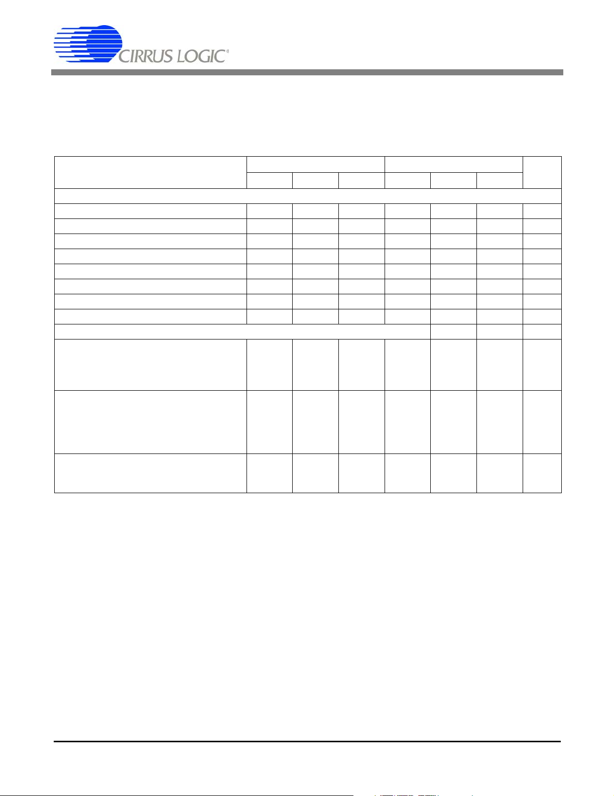
1. CHARACTERISTICS AND SPECIFICATIONS
CS5521/22/23/24/28
ANALOG CHARACTERISTICS (T
= 25° C; VA+, VD+ = 5 V ±5%; VREF+ = 2.5 V, VREF- = AGND,
A
NBV = -2.1 V, XIN = 32.768 kHz, CFS1-CFS0 = ‘00’, OWR (Output Word Rate) = 15 Sps, Bipolar Mode, Input
Range = ±100 mV; See Notes 1 and 2.)
CS5521/23 CS5522/24/28
Parameter
UnitMin Typ Max Min Typ Max
Accuracy
Resolution - - 16 - - 24 Bits
Linearity Error - ±0.0015 ±0.003 - ±0.0007 ±0.0015 %FS
Bipolar Offset (Note 3) - ±1±2 -±16 ±32 LSB
Unipolar Offset (Note 3) - ±2 ±4-±32 ±64 LSB
Offset Drift (Notes 3 and 4) - 20 - - 20 - nV/°C
Bipolar Gain Error - ±8 ±31 - ±8 ±31 ppm
Unipolar Gain Error - ±16 ±62 - ±16 ±62 ppm
Gain Drift (Note 4) - 1 3 - 1 3 ppm/°C
Power Supplies
Power Supply Currents (Normal Mode)
(Note 5)I
I
I
A+
D+
NBV
-
-
-
1.0
90
400
1.4
135
570
-
-
-
1.5
90
525
1.9
135
700
mA
µA
µA
Power Consumption (Note 6)
Normal Mode
Low Power Mode
Standby
Sleep
-
N/A
-
-
6.0
N/A
1.2
500
8.9
N/A
-
-
-
-
-
-
9
5.5
1.2
500
12
7.5
-
-
mW
mW
mW
µW
Power Supply Rejection
Positive Supplies
dc NBV
-
-
120
110
-
-
-
-
120
110
-
-
dB
dB
N
N
Notes: 1. Applies after system calibration at any temperature within -40° C ~ +85° C.
2. Specifications guaranteed by design, characterization, and/or test.
3. Specif ica tio n ap plies to th e de vice on ly and do es not inc lud e an y eff ec ts by ex te rn al para sitic
thermocouples. LSB
: N is 16 for the CS5521/23 and N is 24 for the CS5522/24/28
N
4. Drift over specified temperature range after calibration at power-up at 25° C.
5. Measured with Charge Pump Drive off.
6. All outputs unloaded. All input CMOS levels and the CS5521/23 do not have a low power mode.
DS317F4 5
Page 6
CS5521/22/23/24/28
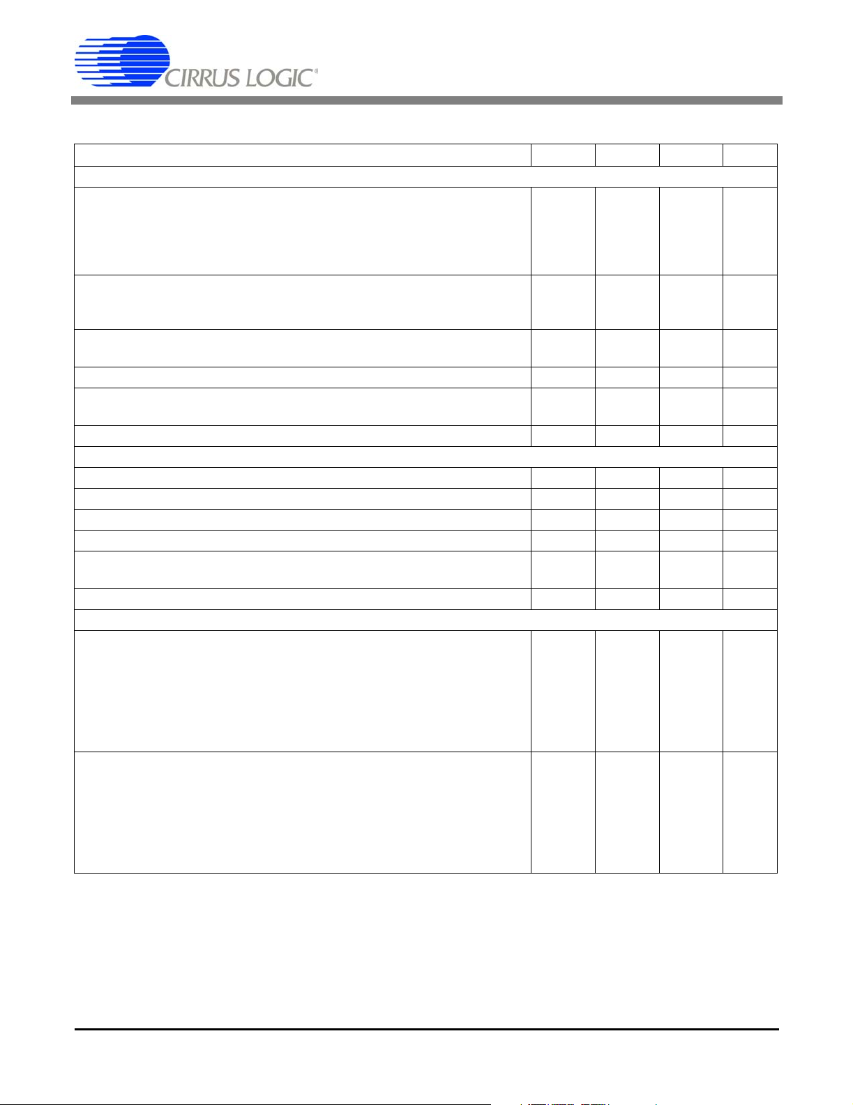
ANALOG CHARACTERISTICS (Continued)
Parameter Min Typ Max Unit
Analog Input
Common Mode + Signal on AIN+ or AIN- Bipolar/Unipolar Mode
NBV = -1.8 to -2.5 V Range = 25 mV, 55 mV, or 100 mV
Range = 1 V , 2.5 V, or 5 V
NBV = AGND Range = 25 mV, 55 mV, or 100 mV (Note 7)
Range = 1 V , 2.5 V, or 5 V
CVF Current on AIN+ or AIN- (Note 8)
Range = 25 mV, 55 mV, or 100 mV
Range = 1 V , 2.5 V, or 5 V
Input Current Drift (Note 8)
Range = 25 mV, 55 mV, or 100 mV - 1 - pA/°C
Input Leakage for Multiplexer when Off - 10 - pA
Common Mode Rejection dc
50, 60 Hz
Input Capacitance - 10 - pF
Voltage Reference Input
Range (VREF+) - (VREF-) 1 2.5 VA+ V
VREF+
VREF- NBV CVF Current (Note 8) - 5.0 - n A
Common Mode Rejection dc
50, 60 Hz
Input Capacitance - 16 - pF
System Calibration Specifications
Full Scale Calibration Range (VREF = 2.5V) Bipolar/Unipolar Mode
25 mV
55 mV
100 mV
1 V
2.5 V
5 V
Offset Calibration Range Bipolar/Unipolar Mode
25 mV
55 mV
100 mV (Note 9)
1 V
2.5 V
5 V
-0.150
NBV
1.85
0.0
-
-
-
-
(VREF-)+1
-
-
10
25
40
0.40
1.0
2.0
-
-
-
-
-
-
-
-
-
-
100
10
120
120
-VA+V
110
130
-
-
-
-
-
-
-
-
-
-
-
-
0.950
VA+
2.65
VA+
300
-
-
-
(VREF+)-1
-
-
32.5
71.5
105
1.30
3.25
VA+
±12.5
±27.5
±50
±0.5
±1.25
±2.50
pA
nA
dB
dB
dB
dB
mV
mV
mV
mV
mV
mV
V
V
V
V
V
V
V
V
V
V
V
Notes: 7. For the CS5528, the 25 mV, 55 mV and 100 mV ranges cannot be used unless NBV is powered at -1.8
to -2.5 V
8. See the section of the data sheet which discusses input models. Chop clock is 256 Hz (XIN/128) for
PGIA (programmable gain instrumentation amplifier). XIN = 32.768 kHz.
9. The maximum full scale signal can be limited by saturation of circuitry within the internal signal path.
6 DS317F4
Page 7

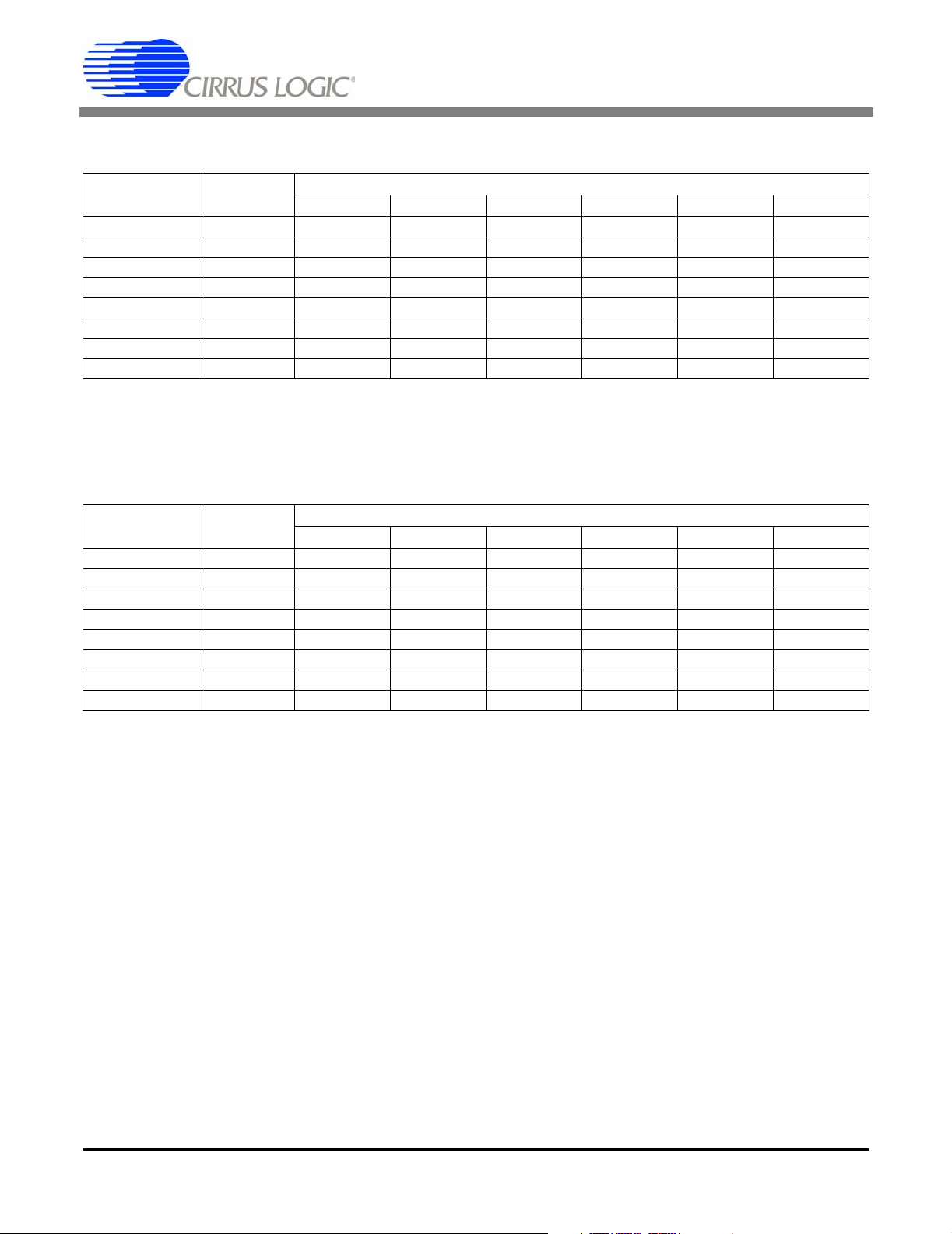
TYPICAL RMS NOISE, CS5521/23 (Notes 10 and 11)
CS5521/22/23/24/28
Output Rate
(Sps)
1.88 1.64 90 nV 148 nV 220 nV 1.8 µV 3.9 µV 7.8 µV
3.76 3.27 122 nV 182 nV 310 nV 2.6 µV 5.7 µV 11.3 µV
7.51 6.55 180 nV 267 nV 435 nV 3.7 µV 8.5 µV 18.1 µV
15.0 12.7 280 nV 440 nV 810 nV 5.7 µV 14 µV 28 µV
30.0 25.4 580 nV 1.1 µV 2.1 µV 18.2 µV 48 µV 96 µV
61.6 (Note 12) 50.4 2.6 µV 4.9 µV 8.5 µV 92 µV 238 µV 390 µV
84.5 (Note 12) 70.7 11 µV 27 µV 43 µV 458 µV 1.1 mV 2.4 mV
101.1 (Note 12) 84.6 41 µV 72 µV 130 µV 1.2 mV 3.4 mV 6.7 mV
Notes: 10. Wideband noise aliased into the baseband. Referred to the input. Typical values shown for 25° C.
11. To estimate Peak-to-Peak Noise, multiply RMS noise by 6.6 for all ranges and output rates.
12. For input ranges <100 mV and output rates ≥60Sps, 16.384 kHz chopping frequency is used.
-3 dB Filter
Frequency
25 mV 55 mV 100 mV 1 V 2.5 V 5 V
Input Range, (Bipolar/Unipolar Mode)
TYPICAL NOISE FREE RESOLUTION (BITS), CS5521/23 (Note 13)
Output Rate
(Sps)
1.88 1.64 16 16 16 16 16 16
3.76 3.27 16 16 16 16 16 16
7.51 6.55 15 16 16 16 16 16
15.0 12.7 15 15 15 16 16 16
30.0 25.4 14 14 14 14 14 14
61.6 (Note 12) 50.4 12 12 12 12 12 12
84.5 (Note 12)70.7999999
101.1 (Note 12)84.6888888
-3 dB Filter
Frequency
25 mV 55 mV 100 mV 1 V 2.5 V 5 V
Input Range, (Bipolar Mode)
Notes: 13. For bipolar mode, the number of bits of Noise Free Resolution is LOG((2XInput Range)/(6.6xRMS
Noise))/LOG(2) rounded to the nearest bit. For unipolar mode, the number of bits of Noise Free
Resolution is LOG((Input Range)/(6.6xRMS Noise))/LOG(2) rounded to the nearest bit. Also, the
CS5521/23’s output conversions are 16 bits. Noise free Resolution numbers are based upon
VREF = 2.5 V and XIN = 32.768 kHz. The values will be affected directly by changes in VREF, but the
effects due to changes in the XIN frequency will be minor.
DS317F4 7
Page 8
TYPICAL RMS NOISE, CS5522/24/28 (Notes 14 and 15)
CS5521/22/23/24/28
Output Rate
(Sps)
1.88 1.64 90 nV 95 nV 140 nV 1.5 µV 3 µV 6 µV
3.76 3.27 110 nV 130 nV 190 nV 2 µV 4 µV 8 µV
7.51 6.55 170 nV 200 nV 275 nV 2.5 µV 6 µV 11.5 µV
15.0 12.7 250 nV 330 nV 580 nV 4.5 µV 10 µV 20 µV
30.0 25.4 500 nV 1 µV 1.5 µV 16 µV 45 µV 85 µV
61.6 (Note 16) 50.4 2 µV 4 µV 8 µV 72 µV 195 µV 350 µV
84.5 (Note 16) 70.7 10 µV 20 µV 35 µV 340 µV 900 µV 2 mV
101.1 (Note 16) 84.6 30 µV 60 µV 105 µV 1.1 mV 3 mV 5.3 mV
Notes: 14. Wideband noise aliased into the baseband. Referred to the input. Typical values shown for 25° C.
15. To estimate Peak-to-Peak Noise, multiply RMS noise by 6.6 for all ranges and output rates.
16. For input ranges <100 mV and output rates ≥60 Sps, 16.384 kHz chopping frequency is used.
-3 dB Filter
Frequency
25 mV 55 mV 100 mV 1 V 2.5 V 5 V
Input Range, (Bipolar/Unipolar Mode)
TYPICAL NOISE FREE RESOLUTION (BITS), CS5522/24/28 (Note 17)
Output Rate
(Sps)
1.88 1.64 16 17 18 18 18 18
3.76 3.27 16 17 17 17 18 18
7.51 6.55 15 16 17 17 17 17
15.0 12.7 15 16 16 16 16 16
30.0 25.4 14 14 14 14 14 14
61.6 (Note 16) 50.4 12 12 12 12 12 12
84.5 (Note 16) 70.7 10 10 10 10 10 10
101.1 (Note 16)84.6888888
-3 dB Filter
Frequency
25 mV 55 mV 100 mV 1 V 2.5 V 5 V
Input Range, (Bipolar Mode)
Notes: 17. For bipolar mode, the number of bits of Noise Free Resolution is LOG((2XInput Range)/(6.6xRMS
Noise))/LOG(2) rounded to the nearest bit. For unipolar mode, the number of bits of Noise Free
Resolution is LOG((Input Range)/(6.6xRMS Noise))/LOG(2) rounded to the nearest bit. Also, the
CS5522/24/28’s output conversions are 24 bits. Noise free Resolution numbers are based upon
VREF = 2.5 V and XIN = 32.768 kHz. The values will be affected directly by changes in VREF, but the
effects due to changes in the XIN frequency will be minor.
8 DS317F4
Page 9

CS5521/22/23/24/28
5 V DIGITAL CHARACTERISTICS (T
= 25° C; VA+, VD+ = 5 V ±5%; GND = 0;
A
See Notes 2 and 18.))
Parameter Symbol Min Typ Max Unit
High-level Input Voltage All Pins Except XIN and SCLK
XIN
SCLK
Low-level Input Voltage All Pins Except XIN and SCLK
XIN
SCLK
High-level Output Voltage
All Pins Except CPD and SDO (Note 19)
CPD, I
SDO, I
= -4.0 mA
out
= -5.0 mA
out
Low-level Output Voltage
All Pins Except CPD and SDO, I
CPD, I
SDO, I
= 1.6 mA
out
= 2 mA
out
= 5.0 mA
out
Input Leakage Current I
3-state Leakage Current I
Digital Output Pin Capacitance C
Notes: 18. All measurements performed under static conditions.
19. I
= -100 µA unless stated otherwise. (VOH = 2.4 V @ I
out
V
IH
V
IL
V
OH
V
OL
in
OZ
out
(VD+) - 0.45
= -40 µA.)
out
0.6 VD+
(VD+)-0.5
-
-
-
(VA+) - 1.0
(VD+) - 1.0
(VD+) - 1.0
-
-
-
-
-
-
-
-
-
-
-
-
-
-
-
-
-
-
0.8
1.5
0.6
-
-
-
0.4
0.4
0.4
V
V
V
V
V
V
V
V
V
V
V
V
-±1±10µA
--±10µA
-9-pF
3 V DIGITAL CHARACTERISTICS (T
= 25° C; VA+ = 5 V ±5%; VD+ = 3.0 V ±10%; GND = 0;
A
See Notes 2 and 18.)
Parameter Symbol Min Typ Max Unit
High-level Input Voltage All Pins Except XIN and SCLK
XIN
SCLK
Low-level Input Voltage All Pins Except XIN and SCLK
XIN
SCLK
High-level Output Voltage
All Pins Except CPD and SDO, I
CPD, I
SDO, I
= -400 µA
out
= -4.0 mA
out
= -5.0 mA
out
Low-level Output Voltage
All Pins Except CPD and SDO, I
CPD, I
SDO, I
= 400 µA
out
= 2 mA
out
= 5.0 mA
out
Input Leakage Current I
3-state Leakage Current I
Digital Output Pin Capacitance C
V
IH
0.6 VD+
(VD+)-0.5
(VD+) - 0.45
V
IL
-
-
-
V
OH
(VA+) - 0.3
(VD+) - 1.0
(VD+) - 1.0
V
OL
-
-
-
in
OZ
out
-±1±10µA
--±10µA
-9-pF
-
-
-
-
-
-
-
-
-
-
-
-
-
-
-
0.16 VD+
0.3
0.6
-
-
-
0.3
0.4
0.4
V
V
V
V
V
V
V
V
V
V
V
V
DS317F4 9
Page 10
DYNAMIC CHARACTERISTICS
Parameter Symbol Ratio Unit
Modulator Sampling Frequency f
Filter Settling Time to 1/2 LSB (Full-scale Step) t
CS5521/22/23/24/28
s
s
XIN/4 Hz
1/f
out
s
RECOMMENDED OPERATING CONDITIONS
(AGND, DGND = 0 V; See Note 20.)
Parameter Symbol Min Typ Max Unit
DC Power Supplies Positive Digital
Positive Analog
Analog Reference V oltage (VREF+) - (VREF-) VRef
VD+
VA+
diff
2.7
4.75
5.0
5.0
5.25
5.25
1.0 2.5 VA+ V
V
V
Negative Bias Voltage NBV -1.8 -2.1 -2.5 V
Notes: 20. All voltages with respect to ground.
ABSOLUTE MAXIMUM RATINGS (AGND, DGND = 0 V; See Note 20.)
Parameter Symbol Min Typ Max Unit
DC Power Supplies (Note 21)
Positive Digital
Positive Analog
Negative Bias Voltage Negative Potential NBV +0.3 -2.1 -3.0 V
Input Current, Any Pin Except Supplies (Note 22 and 23) I
Output Current I
Power Dissipation (Note 24) PDN - - 500 mW
Analog Input Voltage VREF pins
AIN Pins
Digital Input Voltage V
Ambient Operating Temperature T
Storage Temperature T
VD+
VA+
IN
OUT
V
INR
V
INA
IND
A
stg
-0.3
-0.3
-
-
+6.0
+6.0
V
V
--±10mA
--±25mA
NBV -0.3
NBV -0.3
--(VA+) + 0.3
(VA+) + 0.3VV
-0.3 - (VD+) + 0.3 V
-40 - 85 °C
-65 - 150 °C
Notes: 21. No pin should go more negative than NBV - 0.3 V.
22. Applies to all pins including continuous overvoltage conditions at the analog input (AIN) pins.
23. Transient current of up to 100 mA will not cause SCR latch-up. Maximum input current for a power
supply pin is ±50 mA.
24. Total power dissipation, including all input currents and output currents.
WARNING: Operation at or beyond these limits may result in permanent damage to the device.
Normal operation is not guaranteed at these extremes.
10 DS317F4
Page 11
CS5521/22/23/24/28
SWITCHING CHARACTERISTICS (T
Levels: Logic 0 = 0 V, Logic 1 = VD+; C
= 50 pF.))
L
= 25° C; VA+ = 5 V ±5%; VD+ = 3.0 V ±10% or 5 V ±5%;
A
Parameter Symbol Min Typ Max Unit
Master Clock Frequency (Note 25)
External Clock or Internal Oscillator (CS5522/24/28)
(CS5521/23)
XIN
30
30
32.768
32.768
200
130
kHz
kHz
Master Clock Duty Cycle 40 - 60 %
Rise Times (Note 26)
Any Digital Input Except SCLK
SCLK
Any Digital Output
Fall Times (Note 26)
Any Digital Input Except SCLK
SCLK
Any Digital Output
t
rise
t
fall
-
-
-
-
-
-
-
-
50
-
-
50
1.0
100
-
1.0
100
-
µs
µs
ns
µs
µs
ns
Start-up
Oscillator Start-up Time XTAL = 32.768 kHz (Note 27) t
Power-on Reset Period t
ost
por
-500-ms
- 2006 - XIN
cycles
Serial Port Timing
Serial Clock Frequency SCLK 0 - 2 MHz
SCLK Falling to CS
Falling for continuous running SCLK
t
0
100 - - ns
(Note 28)
Serial Clock Pulse Width High
Pulse Width Low
t
1
t
2
250
250
-
-
-
-
ns
ns
SDI Write Timing
CS
Enable to Valid Latch Clock t
Data Set-up Time prior to SCLK rising t
Data Hold Time After SCLK Rising t
SCLK Falling Prior to CS
Disable t
3
4
5
6
50 - - ns
50 - - ns
100 - - ns
100 - - ns
SDO Read Timing
CS
to Data Valid t
SCLK Falling to New Data Bit t
CS
Rising to SDO Hi-Z t
7
8
9
--150ns
--150ns
--150ns
Notes: 25. Device parameters are specified with a 32.768 kHz clock; however, clocks up to 200 kHz
(CS5522/24/28) or 130 kHz (CS5521/23) can be used for increased throughput.
26. Specified using 10% and 90% points on waveform of interest. Output loaded with 50 pF.
27. Oscillator start-up time varies with crystal parameters. This specification does not apply when using an
external clock source.
28. Applicable when SCLK is continuously running.
Specifications are subject to change without notice.
DS317F4 11
Page 12

CS
CS
SCLK
CS5521/22/23/24/28
t
0
t
t
t
3
1
t
2
Figure 1. Continuous Running SCLK Timing (Not to Scale)
t
3
6
CS
SDO
SCLK
SCLK
t
7
MSB
MSB
MSB-1 LSBSDI
t
4
Figure 2. SDI Write Timing (Not to Scale)
t
5
t
1
t
2
t
6
t
9
MSB-1 LSB
t
8
t
2
t
1
Figure 3. SDO Read Timing (Not to Scale)
12 DS317F4
Page 13
2. GENERAL DESCRIPTION
CS5521/22/23/24/28
The CS5521/22/23/24/28 are highly integrated ∆Σ
Analog-to-Digital Converters (ADCs) which use
charge-balance techniques to achieve 16-bit
(CS5521/23) and 24-bit (CS5522/24/28) performance. The ADCs
come as either two-channel
(CS5521/22), four-channel (CS5523/24), or eightchannel (CS5528) devices, and include a low input
current, chopper-stabilized instrumentation amplifier. To permit selectable input spans of 25 mV,
55 mV, 100 mV, 1 V, 2.5 V, and 5 V, the ADCs include a PGA (programmable gain amplifier). To
accommodate ground-based thermocouple applications, the devices include a CPD (Charge Pump
Drive) which provides a negative bias voltage to
the on-chip amplifiers.
These devices also include a fourth order DS modulator followed by a digital filter
eight selectable output word rates of
which provides
1.88 Sps,
3.76 Sps, 7.51 Sps, 15 Sps, 30 Sps, 61.6 Sps,
84.5 Sps, and 101.1 Sps
(XIN = 32.768 kHz).
The
devices are capable of producing output update
rates up to 617 Sps when a 200 kHz clock is used
(CS5522/24/28) or up to 401 Sps using a 130 kHz
clock (CS5521/23). Further note that the digital fil-
ters are designed to settle to full accuracy within
one conversion cycle and simultaneously reject
both 50 Hz and 60 Hz interference when operated
at word rates below 30 Sps (assuming a XIN clock
frequency of 32.768 kHz).
To ease communication between the ADCs and a
micro-controller, the converters include an easy to
use three-wire serial interface which is SPI™ and
Microwire™ compatible.
2.1 Analog Input
Figure 4 illustrates a block diagram of the analog input signal path inside the CS5521/22/23/24/28. The
front end consists of a multiplexer (break before
make configuration), a chopper-stabilized instrumentation amplifier with fixed gain of 20X,
coarse/fine charge buffers, and a programmable gain
section. For the 25 mV, 55 mV, and 100 mV input
ranges, the input signals are amplified by the 20X instrume ntati on amp lifi er. For the 1 V, 2.5 V, and 5 V
input ranges, the instrumentation amplifier is bypassed and the input signals are connected to the
Programmable Gain block via coarse/fine charge
buffers.
NBV
CS5522
IN+
M
U
IN-
X
CS5524
IN+
M
*
U
*
X
*
CS5528
M
*
U
*
X
*
IN+
IN-
IN-
IN+
IN-
Figure 4. Multiplexer Configurations
X20
Programmable
Gain
NBV also supplies the negative
supply voltage for the coarse/fine
change buffers
VREF+
Differential
4th
delta-
modulator
VREF-
order
sigma
Digital
Filter
AIN2+
AIN2-
AIN1+
AIN1-
AIN4+
AIN4-
AIN1+
AIN1-
AIN8+
AIN7+
AIN1+
DS317F4 13
Page 14
CS5521/22/23/24/28
2.1.1 Instrumentation Amplifier
The instrumentation amplifier is chopper stabilized
and is activated any time conversions are performed
with the low-level input ranges, ≤100 mV. The amplifier is powered from VA+ and from the NBV
(Negative Bias Voltage) pin allowing the
CS5521/22/23/24/28 to be operated in either of two
analog input configurations. The NBV pin can be biased to a negative voltage between -1.8 V and
-2.5 V, or tied to AGND (for the CS5528, NBV has
to be between -1.8 V and -2.5 V for the ranges below
100 mV when the amplifier is engaged). The common-mode-plus-signal range of the instrumentation
amplifier is 1.85 V to 2.65 V with NBV grounded.
The common-mode-plus-signal range of the instrumentation amplifier is -0.150 V to 0.950 V with
NBV between -1.8 V to -2.5 V. Whether NBV is
tied between -1.8 V and -2.5 V or tied to AGND,
the (Common Mode + Signal) input on AIN+ and
AIN- must stay between NBV and VA+.
Figure 5 illustrates an analog input model for the
ADCs when the instrumentation amplifier is engaged. The CVF (sampling) input current for each
of the analog input pins depends on the CFS1 and
CFS0 (Chop Frequency Select) bits in the configuration register (see Configuration Register for details). Note that the CVF current is lowest with the
CFS bits in their default states (cleared to logic 0s).
Further note that the CVF current into the instrumentation amplifier is less than 300 pA over -40°C
to +85°C. Note that Figure 5 is for input current
modeling only. For physical input capacitance see
‘Input Capacitance’ specification under ANALOG
CHARACTERISTICS. Also refer to Applications
Note AN30 - “Switched-Capacitor A/D Converter
Input Structures” for more details on input models
and input sampling currents.
Note: Residual noise appears in the converter’s baseband for
output word rates greater than 61.6 Sps if the CFS bits
are logic 0 (chop clock = 256 Hz). For word rates of
30 Sps and lower, 256 Sps chopping is recommended,
and for 61.6 Sps, 84.5 Sps and 101.1 Sps word rate settings, 4096 Hz chopping is recommended.
2.1.2 Coarse/Fine Charge Buffers
The unity gain buffers are activated any time conversions are performed with the high-level inputs ranges, 1 V, 2.5 V, and 5 V. The un ity gain buf fers are
designed to accommodate rail-to-rail input signals.
The common-mode-plus-signal range for the unity
gain buffer amplifier is NBV to VA+.
Typical CVF (sampling) current for the unity gain
buffer amplifiers is about 10 nA
(XIN = 32.768 kHz, see Figure 6).
25 m V, 55 mV, and 100 mV Ranges
AIN
V≤25 mV
os
i=fV C
osn
CFS1/CFS0 = 00, f = 256 Hz
CFS1/CFS0 = 01, f = 4096 Hz
CFS 1/CFS0 = 10, f = 16.384 kHz
CFS1/CFS0 = 11, f = 1024 Hz
Figure 5. Input Models for AIN+ and AIN- pins, ≤(100
mV Input Ranges
14 DS317F4
C=48pF
V≤25 mV
os
i=fV C
Figure 6. Input Models for AIN+ and AIN- pins, >100
1 V, 2.5 V and 5 V Ranges
AIN
osn
,
φ
Fine
1
φ
Coarse
1
C=20pF
f=32.768 kHz
mV input ranges
Page 15
CS5521/22/23/24/28
2.1.3 Analog Input Span Considerations
The CS5521/22/23/24/28 is designed to measure
full-scale ranges of 25 mV, 55 mV, 100 mV, 1 V,
2.5 V, and 5 V. Other full scale values can be accommodated by performing a system calibration
within the limits specified. See the Calibration section for more details. Another way to change the
full scale range is to increase or to decrease the
voltage reference to a voltage other than 2.5 . See
the Voltage Reference section for more details.
Three factors set the operating limits for the input
span. They include: instrumentation amplifier saturation, modulator 1’s density, and a lower reference
voltage. When the 25 mV, 55 mV, or 100 mV
range is selected, the input signal (including the
common-mode voltage and the amplifier offset
voltage) must not cause the 20X amplifier to saturate in either its input stage or output stage. To prevent saturation, the absolute voltages on AIN+ and
AIN- must stay within the limits specified (refer to
the Analog Input section). Additionally, the differential output voltage of the amplifier must not exceed 2.8 V. The equation
is the differential input voltage and VOS is the absolute maximum offset voltage for the instrumentation amplifier (VOS will not exceed 40 mV). If the
differential output voltage from the amplifier exceeds 2.8 V, the amplifier may saturate, which will
cause a measurement error.
The input voltage into the modulator must not
cause the modulator to exceed a low of 20 percent
or a high of 80 percent 1's density. The nominal
full-scale input span of the modulator (from 30 percent to 70 percent 1’s density) is determined by the
VREF voltage divided by the Gain Factor. See
Table 1
to determine if the CS5521/22/23/24/28 is
being used properly. For example, in the 55 mV
range, to determine the nominal input voltage to the
modulator, divide VREF (2.5 V) by the Gain Factor (2.2727).
When a smaller voltage reference is used, the resulting code widths are smaller causing the converter output codes to exhibit more changing codes
for a fixed amount of noise. Table 1 is based upon
a VREF = 2.5 V. For other values of VREF, the
values in Table 1 must be scaled accordingly.
ABS(VIN + VOS) x 20 = 2.8 V
defines the differential output limit, where
VIN = (AIN+) - (AIN-)
Input Range
± 25 mV
± 55 mV
± 100 mV
± 1.0 V - 2.5V 2.5 ± 1.0 V ± 1.5 V
± 2.5 V - 2.5V 1.0 ± 2.5 V ± 5.0 V
± 5.0 V - 2.5V 0.5 ± 5.0 V 0V, VA+
Note: 1. The converter's actual input range, the delta-sigma's nominal full-scale input, and the delta -sig m a's
(1)
Table 1. Relationship between Full Scale Input, Gain Factors, and Internal Analog
maximum full-scale input all scale directly with the value of the voltage reference. The values in the
table assume a 2.5
2. The 2.8 V limit at the output of the 20X amplifier is the differential output voltage.
Max. Differential Output
20X Amplifier
(2)
2.8 V
(2)
2.8 V
(2)
2.8 V
V VREF voltage.
Signal Limitations
2.1.4 Measuring Voltages Higher than 5 V
Some systems require the measurement of voltages
greater than 5 V. The input current of the instru-
VREF Gain Factor
2.5V 5 ± 0.5 V ± 0.75 V
2.5V 2.272727... ± 1.1 V ± 1.65 V
2.5V 1.25 ± 2.0 V ± 3.0 V
∆-Σ Nominal
Differential Input
(1)
(1)
∆-Σ
Max. Input
DS317F4 15
Page 16
CS5521/22/23/24/28
mentation amplifier, typically 100 pA, is low
enough to permit large external resistors to divide
down a large external signal without significant
loading. Figure 7 illustrates an example circuit. Refer to Application Note 158 for more details on
high-voltage (>5 V) measurement.
2.1.5 Voltage Reference
The CS5521/22/23/24/28 devices are specified for
operation with a 2.5 V reference voltage between
the VREF+ and VREF- pins of the device. For a
single-ended reference voltage, such as the
LT1019-2.5, the reference voltage is input into the
VREF+ pin of the converter and the VREF- pin is
grounded.
The differential voltage between the VREF+ and
VREF- can be any voltage from 1.0 V up to VA+,
however, the VREF+ cannot go above VA+ and the
VREF- pin can not go below NBV.
10
VA+
+
PGIA
-
Ω
0.1 µF
VD+
∆Σ
ADC
±10V
+5 V
1 M
Voltage
Divider
0.1 µF
10 K
VREF+
VREF-
Ω
2.5 V
Ω
Figure 8 illustrates the input models for the VREF
pins. The dynamic input current for each of the pins
can be determined from the models shown.
2.2 Overview of ADC Register Structure and Operating Modes
The CS5521/22/23/24/28 ADCs have an on-chip
controller, which includes a number of user-accessible registers. The registers are used to hold offset
and gain calibration results, configure the chip's
operating modes, hold conversion instructions, and
to store conversion data words. Figure 9 depicts a
block diagram of the on-chip controller’s internal
registers for the CS5523/24.
Each of the converters has 24-bit registers to function as offset and gain calibration registers for each
channel. The converters with two channels have
two offset and two gain calibration registers, the
converters with four channels have four offset and
four gain calibration registers, and the eight channel converter has eight offset and eight gain calibration registers. These registers hold calibration
results. The contents of these registers can be read
or written by the user. This allows calibration data
to be off-loaded into an external EEPROM. The
user can also manipulate the contents of these registers to modify the offset or the gain slope of the
converter.
The converters include a 24-bit configuration register of which 17 of the bits are used for setting options such as the conversion mode, operating power
options, setting the chop clock rate of the instru-
PGIA set for
100 mV
+
chop clock = 256 Hz
NBV
≈
-2.1 V
V
Charge Pump
Regulator
1N4148
µ
F
10
+
CPD
0.033
1N4148BAT85
µ
F
Figure 7. Input Ranges Greater than 5 V
DGND
Charge Pump
Circuitry
VREF
V ≤ 25mV
os
i = fV C
osn
f = 32.768 kHz
Figure 8. Input Model for VREF+ and VREF- Pins
Fin e
φ
1
Coarse
φ
2
C = 10pF
16 DS317F4
Page 17
CS5521/22/23/24/28
mentation amplifier, and providing a number of
flags which indicate converter operation.
A group of registers, called Channel Set-up Registers, are also included in the converters. These registers are used to hold pre-loaded conversion
instructions. Each channel set-up register is 24 bits
wide and holds two 12-bit conversion instructions
(Setups). Upon power-up, these registers can be
initialized by the user’s microcontroller with conversion instructions. The user can then use bits in
the configuration register to choose a conversion
mode.
Several conversion modes are possible. Using the
single conversion mode, an 8-bit command word
can be written into the serial port. The command includes pointer bits which ‘point’ to a 12-bit command in one of the Channel Setup Registers which
is to be executed. The 12-bit commands can be setup to perform a conversion on any of the input
channels of the converter. More than one of the 12bit Setups can be used for the same analog input
channel. This allows the user to convert on the
same signal with either a different conversion
speed, a different gain range, or any of the other options available in the Setup Register. The user can
set up the registers to perform conversions using
different conversion options on each of the input
channels.
The ADCs also include multiple-channel conversion capability. User bits in the configuration register of the ADCs can be configured to sequence
through the 12-bit command Setups, performing a
conversion according to the content of each 12-bit
Setup. This channel scanning capability can be
configured to run continuously, or to scan through
a specified number of Setup Registers and stop until commanded to continue. In the multiple-channel
scanning modes, the conversion data words are
loaded into an on-chip data FIFO. The converter issues a flag on the SDO pin when a scan cycle is
completed so the user can read the FIFO. More details are given in the following pages.
Instructions are provided on how to initialize the
converter, perform offset and gain calibrations, and
to configure the converter for the various conversion modes. Each of the bits of the configuration
register and of the Channel Setup Registers is described. A list of examples follows the description
section. Table 2 can be used to decode all valid
commands (the first 8 bits into the serial port).
4 (24) 4 (24) 4 (12 x 2) 8 x 24
AIN1
AIN2
AIN3
AIN4
Off 1
Off 2
Off 3
Off 4
1 x 24
Configuration
Chop Frequency
Multiple Conversions
Depth Pointer
Loop
Read Convert
Powerdown Modes
Flags
Etc.
Figure 9. CS5523/24 Register Diagram
Gain 1
Gain 2
Gain 3
Gain 4
Setup 1
Setup 3
Setup 5
Setup 7
Setup 2
Setup 4
Setup 6
Setup 8
Latch Outputs
Channel Select
Output Word Rate
PGA Selection
Unipolar/Bipolar
DATA
FIFO
SDO
DS317F4 17
Page 18

CS5521/22/23/24/28
2.2.1 System Initialization
When power to the CS5521/22/23/24/28 is applied,
the chips are held in a reset condition until the
32.768 kHz oscillator has started and a countertimer elapses. Due to the high Q of the 32.768 kHz
crystal, the oscillator takes 400-600 ms to start. The
counter-timer counts 2006 oscillator clock cycles
to make sure the oscillator is fully stable. During
this time-out period, the serial port logic is reset
and the RV (Reset Valid) bit in the configuration
register is set to indicate that a valid reset occurred.
After a reset, the on-chip registers are initialized to
the following states and the converter is placed in
the command mode where it waits for a valid command.
configuration register: 000040(H)
offset registers: 000000(H)
gain registers: 400000(H)
channel setup registers: 000000(H)
Note: A system reset can be initiated at any time by writing
a logic 1 to the RS (Reset System) bit in the configuration register. After a reset, the RV bit is set until the
configuration register is read. The user must then
write a logic 0 to the RS bit to take the part out of the
reset mode. Any other bits written to the configuration
register at this time will be lost. The configuration register must be written again once RS = 0 to set any other
bits.
2.2.2 Serial Port Initialization Sequence
The serial port is initialized to the command mode
whenever a power-on reset is performed inside the
converter, or when the user transmits the port initialization sequence. The port initialization sequence involves clocking 15 bytes of all 1's,
followed by one byte with the following bit contents ‘1111 1110’. This sequence places the chip in
the command mode where it waits for a valid command to be written.
18 DS317F4
Page 19

CS5521/22/23/24/28
2.2.3 Command Register Quick Reference
D7(MSB)D6D5D4D3D2D1D0
CB CS2 CS1 CS0 R/W
BIT NAME VALUE FUNCTION
D7 Command Bit, CB 0
1
D6-D4 Channel Select Bits,
CSB2-CSB0
D3 Read/Write
D2-D0 Register Select Bit,
RSB2-RSB0
, R/W 0
000
.
.
111
1
000
001
010
011
101
110
111
RSB2 RSB1 RSB0
Must be logic 0 for these commands.
See table below.
CS2-CS0 provide the address of one of the eight physical
channels. These bits are used to access the calibration registers associated with respective channels.
Note: These bits are ignored when reading the data register.
Write to selected register.
Read from selected register.
Reserved
Offset Register
Gain Register
Configuration Register
Channel Set-up Registers
- register is 48-bits long for CS5521/22
- register is 96-bits long for CS5523/24
- register is 192-bits long for CS5528
Reserved
Reserved
D7(MSB)D6D5D4D3D2D1D0
CB CSRP3 CSRP2 CSRP1 CSRP0 CC2 CC1 CC0
BIT NAME VALUE FUNCTION
D7 Command Bit, CB 0
D6-D3 Channel Pointer Bits,
CSRP3-CSRP0
D2-D0 Conversion/Calibration
Bits, CC2-CC0
0000
1111
000
001
010
011
100
101
110
111
1
.
.
.
See table above.
Must be logic 1 for these commands.
These bits are used as pointers to the Setups.
Note: The MC bit, must be logic 0 for these bits to take effect.
When MC = 1, these bits are ignored. The LP, MC, and RC
bits in the configuration register are ignored during calibration.
Normal Conversion
Self-Offset Calibration
Self-Gain Calibration
Reserved
Reserved
System-Offset Calibration
System-Gain Calibration
Reserved
Table 2. Command Register Quick Reference
DS317F4 19
Page 20

CS5521/22/23/24/28
2.2.4 Command Register Descriptions
READ/WRITE INDIVIDUAL OFFSET CALIBRATION REGISTER
D7(MSB) D6 D5 D4 D3 D2 D1 D0
0 CS2 CS1 CS0 R/W
001
Function
: These commands are used to access each offset register separately. CS1 - CS0 decode the
registers accessed.
R/W
(Read/Write)
0 Write to selected register.
1 Read from selected register.
CS[2:0] (Channel Select Bits)
000 Offset Register 1(All devices)
001 Offset Register 2 (All devices)
010 Offset Register 3 (CS5523/24/28 only)
011 Offset Register 4 (CS5523/24/28 only)
100 Offset Register 5 (CS5528 only)
101 Offset Register 6 (CS5528 only)
110 Offset Register 7 (CS5528 only)
111 Offset Register 8 (CS5528 only)
READ/WRITE INDIVIDUAL GAIN REGISTER
D7(MSB) D6 D5 D4 D3 D2 D1 D0
0 CS2 CS1 CS0 R/W
Function
: These commands are used to access each gain register separately. CS1 - CS0 decode the r eg-
010
isters accessed.
(Read/Write)
R/W
0 Write to selected register.
1 Read from selected register.
CS[2:0] (Channel Select Bits)
000 Gain Register 1(All devices)
001 Gain Register 2 (All devices)
010 Gain Register 3 (CS5523/24/28 only)
011 Gain Register 4 (CS5523/24/28 only)
100 Gain Register 5 (CS5528 only)
101 Gain Register 6 (CS5528 only)
110 Gain Register 7 (CS5528 only)
111 Gain Register 8 (CS5528 only)
20 DS317F4
Page 21

CS5521/22/23/24/28
READ/WRITE CONFIGURATION REGISTER
D7(MSB) D6 D5 D4 D3 D2 D1 D0
0000R/W
Function: These commands are used to read from or write to the configuration register.
R/W
(Read/Write)
0 Write to selected register.
1 Read from selected register.
READ/WRITE CHANNEL-SETUP REGISTER(S)
D7(MSB) D6 D5 D4 D3 D2 D1 D0
0000R/W
011
101
Function
: These commands are used to access the channel-setup registers (CSRs). The number of
CSRs accessed is determined by the device being u sed and the number of CSRs that are being
accessed (i.e. the depth bits in the configuration reg iste r de te rm in e th e nu m ber of lev els accessed). This register is 48-bits long (4 Setups) for the CS5521/22, 96-bits long (8 Setups) for
the CS5523/24, and 192-bits (16 Setups) long for the CS5528.
R/W
(Read/Write)
0 Write to selected register.
1 Read from selected register.
DS317F4 21
Page 22

CS5521/22/23/24/28
PERFORM CONVERSION
D7(MSB) D6 D5 D4 D3 D2 D1 D0
1 CSRP3 CSRP2 CSRP1 CSRP0 0 0 0
Function: These commands instruct the ADC to perform conversions on the physical input channel point-
ed to by the pointer bits (CSRP2 - CSRP0) in the channel-setup registers. The particular type
of conversion performed is determined by the states of the conversion contro l bits (the multiple
conversion bit, the loop bit, read convert bit, and the depth pointer bits) in the configuration register.
CSRP [3:0] (Channel Setup Register Pointer Bits)
0000 Setup 1 (All devices)
0001 Setup 2 (All devices)
0010 Setup 3 (All devices)
0011 Setup 4 (All devices)
0100 Setup 5 (CS5523/24/28)
0101 Setup 6 (CS5523/24/28)
0110 Setup 7 (CS5523/24/28)
0111 Setup 8 (CS5523/24/28)
1000 Setup 9 (CS5528 only)
1001 Setup 10 (CS5528 only)
1010 Setup 11 (CS5528 only)
1011 Setup 12 (CS5528 only)
1100 Setup 13 (CS5528 only)
1101 Setup 14 (CS5528 only)
1110 Setup 15 (CS5528 only)
1111 Setup 16 (CS5528 only)
22 DS317F4
Page 23

CS5521/22/23/24/28
PERFORM CALIBRATION
D7(MSB) D6 D5 D4 D3 D2 D1 D0
1 CSRP3 CSRP2 CSRP1 CSRP0 CC2 CC1 CC0
Function: These commands instruct the ADC to perform a calibration on the physical input channel refer-
enced which is chosen by the command byte pointer bits (CSRP3 - CRSP0).
CSRP [3:0] (Channel Setup Register Pointer Bits)
0000 Setup 1 (All devices)
0001 Setup 2 (All devices)
0010 Setup 3 (All devices)
0011 Setup 4 (All devices)
0100 Setup 5 (CS5523/24/28 only)
0101 Setup 6 (CS5523/24/28 only)
0110 Setup 7 (CS5523/24/28 only)
0111 Setup 8 (CS5523/24/28 only)
1000 Setup 9 (CS5528 only)
1001 Setup 10 (CS5528 only)
1010 Setup 11 (CS5528 only)
1011 Setup 12 (CS5528 only)
1100 Setup 13 (CS5528 only)
1101 Setup 14 (CS5528 only)
1110 Setup 15 (CS5528 only)
1111 Setup 16 (CS5528 only)
CC [2:0] (Calibration Control Bits)
000 Reserved
001 Self-Offset Calibration
010 Self-Gain Calibration
011 Reserved
100 Reserved
101 System-Offset Calibration
110 System-Gain Calibration
111 Reserved
DS317F4 23
Page 24

CS5521/22/23/24/28
SYNC1
D7(MSB) D6 D5 D4 D3 D2 D1 D0
11111111
Function: Part of the serial port re-initialization sequence.
SYNC0
D7(MSB) D6 D5 D4 D3 D2 D1 D0
11111110
Function: End of the serial port re-initialization sequence.
NULL
D7(MSB) D6 D5 D4 D3 D2 D1 D0
00000000
Function: This command is used to clear a port flag and keep the converter in the continuous conver sion
mode.
24 DS317F4
Page 25

CS5521/22/23/24/28
2.2.5 Serial Port Interface
The CS5521/22/23/24/28’s serial interface consists
of four control lines: CS, SCLK, SDI, SDO.
Figure 10 illustrates the serial sequence necessary
to write to, or read from the serial port’s registers.
CS
(Chip Select) is the control line which enables
access to the serial port. If the CS
the port can function as a three-wire interface.
SDI (Serial Data In) is the data signal used to transfer data to the converters.
SDO (Serial Data Out) is the data signal used to
transfer output data from the converters. The SDO
CS
SCLK
SDI
pin is tied low,
output will be held at high impedance any time CS
is at logic 1.
SCLK (Serial Clock) is the serial bit clock which
controls the shifting of data to or from the ADC’s
serial port. The CS
pin must be held low (logic 0)
before SCLK transitions can be recognized by the
port logic. To accommodate opto-isolators SCLK
is designed with a Schmitt-trigger input to allow an
opto-isolator with slower rise and fall times to directly drive the pin. Additionally, SDO is capable
of sinking or sourcing up to 5 mA to directly drive
an opto-isolator LED. SDO will have less than a
400 mV loss in the drive voltage when sinking or
sourcing 5 mA.
MSB
LSB
SCLK
SDI
SDO
CS
SCLK
SDI
SDO
Command Time
8 SCLKs
Command T ime
8SCLKs
Command Time
8SCLKs
t *
d
Data Time 24 SCLKs
Write Cycle
MSB
Data Time 24SCLKs
Read Cycle
8 SCLKs Clear SDO Flag
MSB
LSB
XIN/OWR
Clock Cycles
LSB
* td = XIN/OWR cl ock cycles for each convers i o n except the
first conversion which will take XIN/OWR + 7 clock cycles
Figure 10. Command and Data Word Timing
Data Time
24 SCLKs
DS317F4 25
Page 26

CS5521/22/23/24/28
2.2.6 Reading/Writing the Offset, Gain, and Configuration Registers
The CS5521/22/23/24/28’s offset, gain, and configuration registers are accessed individually and can
be read from or written to. To write to an offset, a
gain, or the configuration register, the user must
transmit the appropriate write command which accesses the particular register and then follow that
command with 24 bits of data (refer to Figure 10 for
details). For example, to write 0x800000 (hexadecimal) to physical channel one’s gain register, the user
would transmit the command byte 0x02 (hexadecimal) and then follow that command byte with the
data 0x800000 (hexadecimal). Similarly, to read
physical channel one’s gain register, the user must
first transmit the command byte 0x0A (hexadecimal) and then read the 24 bits of data. Once an offset, a gain, or the configuration register is written to
or read from, the serial p
mode.
2.2.7 R
sters
i
The CS5521/22 have two 24-bit channel-setup registers (CSRs). The CS5523/24 have four CSRs, and
the CS5528 has eight CSRs (refer to Table 3 for
more detail on the CSRs). These registers are accessed in conjunction with the depth pointer bits in
the configuration register. Each CSR contains two
12-bit Setups which are programmed by the user to
contain data conversion or calibration information
such as:
1) state of the output latch pins
2) output word rate
3) gain range
4) polarity
5) the address of a physical input channel to be
eading/Writing the Channel-Setup Reg-
converted.
ort returns to the command
Once programmed, they are used to determine the
mode (e.g. unipolar, 15 Sps, 100 mV range etc.) the
ADC will operate in when future conversions or
calibrations are performed.
To access the CSRs, the user must first initialize the
depth pointer bits in the configuration register as
these bits determine the number of CSRs to read
from or write to. For example, to write CSR1
(Setup1 and Setup2), the user would first program
the configuration register’s depth pointer bits with
‘0001’ binary. This notifies the ADC’s serial port
that only the first CSR is to be accessed. Then, the
user would transmit the write command, 0x05
(hexadecimal) and follow that command with 24
bits of data. Similarly, to read CSR1, the user must
transmit the command byte 0x0D (hexadecimal)
and then read the 24 bits of data. To write more
than one CSR, for instance CSR1 and CSR2
(Setup1, Setup2, Setup3, and Setup4), the user
would first set the depth pointer bits in the configuration register to ‘0011’ binary. The user would then
transmit the write CSR command 0x05 (hexadecimal) and follow that with the information for
Setup1, Setup2, Setup 3, and Setup 4 which is 48
bits of information. Note that while reading/writing
CSRs, two Setups are accessed in pairs as a single
24-bit CSR register. Even if one of the Setups isn’t
used, it must be written to or read. Further note that
the CSRs are accessed as a closed array – the user
can not access CSR2 without accessing CSR1. This
requirement means that the depth bits in the configuration register can only be set to one of the following states when the CSRs are being read from or
written to: 0001, 0011, 0101, 0111, 1001, 1011,
1101, 1111. Examples detailing the power of the
CSRs are provided in the
and Reading the Data Conversion FIFO
Once the CSRs are written to or read from, the serial
port returns to the command
Performing Conversions
section.
mode.
26 DS317F4
Page 27

CS5521/22/23/24/28
CSR (Channel-Setup Register) CSR CSR
#1 Setup 1
Bits <47:36>
#2 Setup 3
Bits <23:12>
CS5521/22 CS5523/24 CS5528
D23(MSB) D22 D21 D20 D19 D18 D17 D16 D15 D14 D13 D12
A1 A0 CS2 CS1 CS0 WR2 WR1 WR0 G2 G1 G0 U/B
D11 D10 D9 D8 D7 D6 D5 D4 D3 D2 D1 D0
A1 A0 CS2 CS1 CS0 WR2 WR1 WR0 G2 G1 G0 U/B
BIT NAME VALUE FUNCTION
D23-D22/
D11-D10
D21-D19/
D9-D7
D18-D16/
D6-D4
D15-D13/
D3-D1
D12/D0 Unipolar/Bipolar, U/B
Latch Outputs, A1-A0 00 *R Latch Output Pins A1-A0 mimic D23/D11-D22/D10 register bits.
Channel Select, CS2CS0
Word Rate, WR2-WR0 000
Gain Bits, G2-G0 000
Setup 2
Bits <35:24>
Setup 4
Bits <11:0>
000
001
010
011
100
101
110
111
001
010
011
100
101
110
111
001
010
011
100
101
110
111
0
1
#1 Setup 1
Bits <95:84>
#4 Setup 7
Bits <23:12>
R Select physical channel 1 (All devices)
Select physical channel 2(All devices)
Select physical channel 3 (CS5523/24/28 only)
Select physical channel 4 (CS5523/24/28 only)
Select physical channel 5 (CS5528 only)
Select physical channel 6 (CS5528 only)
Select physical channel 7 (CS5528 only)
Select physical channel 8 (CS5528 only)
R 15.0 Sps (2180 XIN cycles).
30.0 Sps (1092 XIN cycles).
61.6 Sps (532 XIN cycles).
84.5 Sps (388 XIN cycles).
101.1 Sps (324 XIN cycles).
1.88 Sps (17444 XIN cycles).
3.76 Sps (8724 XIN cycles).
7.51 Sps (4364 XIN cycles).
R 100 mV (assumes VREF Differential = 2.5 V)
55 mV
25 mV
1.0 V
5.0 V
2.5 V
Not used.
Not used.
R Bipolar measurement mode.
Unipolar measurement mode.
Setup 2
Bits <83:72>
Setup 8
Bits <11:0>
#1 Setup1
Bits <191:180>
#8 Setup 15
Bits <23:12>
Setup 2
Bits <179:168>
Setup 16
Bits <11:0>
* R indicates the bit value after the part is reset
Table 3. Channel-Setup Registers
DS317F4 27
Page 28

CS5521/22/23/24/28
2.2.7.1 Latch Outputs
The A1-A0 pins mimic the latch output, D23/D11D22/D10, bits of the channel-setup registers. A1-A0
can be used to control external multiplexers and other logic functions outside the converter. The outputs
can sink or source at least 1 mA, but it is recommended to limit drive currents to less than 20µA to
reduce self-heating of the chip. T
powered from VA+, hence their output voltage for
a logic 1 will be limited to the VA+ supply voltage.
hese outputs are
2.2.7.2 Channel Select Bits
The channel select, CS1-CS0, bits are used to determine which physical input channel will be used
when a conversion is performed with a particular
Setup.
2.2.7.3 Output Word Rate Selection
The word rate, WR2-WR0, bits of the channel-setup registers set the output conversion word rate of
the converter when a conversion is performed with
a particular Setup. The word rates indicated in
Table 3 assume a master clock of 32.768 kHz, and
scale linearly when using other master clock frequencies. Upon reset the converter is set to operate
with an output word rate of 15.0 Sps.
2.2.7.4 Gain Bits
The gain bits, G2-G0, of the channel-setup registers set the full-scale differential input range for the
ADC when a conversion is performed with a particular Setup. The input ranges in the table assume a
2.5 V reference voltage, and scale linearly when
using other reference voltages.
2.2.8 Configuration Register
The configuration register is 24 bits long. The following subsections detail the bits in the configuration register. Table 4 summarizes the configuration
register.
2.2.8.1 Chop Frequency Select
The chop frequency select (CFS1-CFS0) bits are
used to set the rate at which the instrumentation
amplifier’s chop switches modulate the input signal. The 256 Hz rate is desirable as it provides the
lowest input CVF (sampling) current, <300 pA
over -40 to 85 °C. The higher rates can be used to
eliminate modulation/aliasing effects as the frequency of the input signal increases.
2.2.8.2 Conversion/Calibration Control Bits
The conversion/calibration control bits in the configuration register are used to control the particular
type of conversion required for the users applications. In short, the depth pointer (DP3-DP0) bits
determine the number of Setups that will be referenced when conversions are performed. The multiple conversion (MC) bit instructs the converter to
perform conversions on the number of Setups in the
channel-setup registers which are referenced by the
depth pointer bits. The converter begins with
Setup1 and moves sequentially through the Setups
in this mode. The Loop (LP) bit instructs the converter to continuously perform conversions until a
Stop command is sent to the converter. The read
convert (RC) bit instructs the converter to wait until
the conversion data is read before performing the
next conversion or set of conversions.
2.2.7.5 Unipolar/Bipolar Bit
The unipolar/bipolar bit is used to determine the
type of conversion, unipolar or bipolar, that will be
performed with a particular Setup.
28 DS317F4
2.2.8.3 Power Consumption Control Bits
The CS5522/24/28 devices accommodate four
power consumption modes: normal, low power,
standby, and sleep. The CS5521/23 accommodate
three power consumption modes: normal, standby,
and sleep. The normal (default) mode is entered after a power-on reset. In normal mode, the
Page 29

CS5521/22/23/24/28
CS5522/24/28 typically consume 9.0 mW. The
CS5521/23 typically consume 6.0 mW. The lowpower mode is an alternate mode in the
CS5522/24/28 that reduces the consumed power to
5.5 mW. It is entered by setting bit D8 (the lowpower mode bit) in the configuration register to
logic 1. Slightly degraded noise or linearity performance should be expected in the low-power mode.
Note that the XIN clock should not exceed 130 kHz
in low-power mode. The final two modes accommodated in all devices are referred to as the power
save modes. They power down most of the analog
portion of the chip and stop filter convolutions. The
power-save modes are entered whenever the PS/R
bit of the configuration register is set to logic 1. The
particular power-save mode entered depends on
state of bit D11 (PSS, the Power Save Select bit) in
the configuration register. If PSS is logic 0, the
converters enters the standby mode reducing the
power consumption to 1.2 mW. The standby mode
leaves the oscillator and the on-chip bias generator
running. This allows the converter to quickly return
to the normal or low-power mode once the PS/R bit
is set back to a logic 0. If PSS and PS/R in the configuration register are set to logic 1, the sleep mode
is entered reducing the consumed power to around
500 µW. Since the sleep mode disables the oscillator, approximately a 500ms oscillator start-up delay period is required before returning to the
normal or low-power mode.
2.2.8.4 Charge Pump Disable
The pump disable (PD) bit permits the user to turn
off the charge pump drive thus enabling the user to
reduce the radiation of digital interference from the
CPD pin when the charge pump is not being used.
2.2.8.5 Reset System Control Bits
The reset system (RS) bit permits the user to perform a system reset. A system reset can be initiated
at any time by writing a logic 1 to the RS bit in the
configuration register. After a system reset cycle is
complete, the reset valid (RV) bit is set indicating
that the internal logic was properly reset. The RV
remains set until the configuration register is read.
Note that the user must write a logic 0 to the RS bit
to take the part out of the reset mode. No other bits
in the configuration register can be written at this
time. A subsequent write to the configuration register is necessary to write to any other bits in this
register. Once reset, the on-chip registers are initialized to the following states.
configuration register: 000040(H)
offset registers: 000000(H)
gain registers: 400000(H)
channel setup registers: 000000(H)
2.2.8.6 Data Conversion Error Flags
The oscillation detect (OD) and overflow (OF) bits
in the configuration register are flag bits used to indicate that the ADC performed a conversion on an
input signal that was not within the conversion
range of the ADC. For convenience, the OD and
OF bits are also in the data conversion word of the
CS5521/23.
The OF bit is set to logic 1 when the input signal is:
1) more positive than full scale
2) more negative than zero in unipolar mode, or
3) more negative than negative full scale in bipolar mode.
The OF flag is cleared to logic 0 when a conversion
occurs which is not out of range.
The OD bit is set to logic 1 any time that an oscillatory condition is detected in the modulator. This
does not occur under normal operating conditions,
but may occur when the input is extremely overranged. The OD flag will be cleared to logic 0 when
the modulator becomes stable.
DS317F4 29
Page 30

CS5521/22/23/24/28
D23(MSB) D22 D21 D20 D19 D18 D17 D16 D15 D14 D13 D12
NU NU CFS1 CFS0 NU MC LP RC DP3 DP2 DP1 DP0
D11 D10 D9 D8 D7 D6 D5 D4 D3 D2 D1 D0
PSS PD PS/R
BIT NAME VALUE FUNCTION
D23-D22 Not Used, NU 00 R* Must always be logic 0.
D21-D20 Chop Frequen cy Select,
CFS1-CFS0
D19 Not Used, NU 0 R Must always be lo gic 0.
D18 Multiple Conversion, MC 0
D17 Loop, LP 0
D16 Read Convert, RC 0
D15-D12 Depth Pointer, DP3-DP0 0000
D1 1 Power Save Select, PSS 0
D10 Pump Disable, PD 0
D9 Power Save/Run
D8 Low Power Mode, LPM 0
D7 Reset System, RS 0
D6 Reset Valid, RV 0
D5 Oscillation Detect, OD 0
D4 Overrange Flag, OF 0
D3-D0 Not Used, NU 0000 R Must always be logic 0.
LPM RS RV OD OF NU NU NU NU
00
01
10
11
1111
, PS/R 0
R 256 Hz Amplifier chop frequency. (XIN = 32.768 kHz)
4,096 Hz Amplifier chop frequency.
16,384 Hz Amplifier chop frequency.
1,024 Hz Amplifier chop frequency.
R Perform single-Setup conversions. MC bit is ignored during calibrations.
1
1
1
.
.
1
1
1
1
1
1R
1
1
Perform multiple-Setup conversions on Setups in the channel-setup register by issuing only one command with MSB = 1.
R The conversions on the single Setup (MC = 0) or multiple Setups (MC =
1) are performed only once.
The conversions on the single Setup (MC = 0) or multiple Setups (MC =
1) are continuously performed.
R Don’t wait for user to finish reading data before starting new conversions.
The RC bit is used in conjunction with the LP bit when the LP bit is set to
logic 1. If LP = 0, the RC bit is ignored. If LP = 1, the ADC waits for user to
read data conversion(s) before converting again. The RC bit is ignored
during calibrations. Refer to Calibration Protocol for details.
R When writing or reading the CSRs, these bits (DP3-DP0) determine the
number of CSR’s to be accessed (0000=1). They are also used to determine how many Setups are converted when MC=1 and a command byte
with its MSB = 1 is issued. Note that the CS5522 has two CSRS, the
CS5524 has four CSRs, and the CS5528 has 8 CSRs.
R Standby Mode (Oscillator active, allows quick power-up).
Sleep Mode (Oscillator inactive).
R Charge Pump Enabled.
For PD = 1, the CPD pin goes to a Hi-Z output state.
RRun.
Power Save.
R Normal Mode (LPM bit is only for the CS5522/24/28)
Reduced Power Mode
R Normal Operation.
Activate a Reset cycle. To return to Normal Ope r ation write bit to zero.
No reset has occurred or bit has been cleared (read only).
Bit is set after a Valid Reset has occurred. (Cleared when read.)
R Bit is clear when an oscillation condition has not occurred (read only).
Bit is set when an oscillatory condition is detected in the modulator.
R Bit is clear when an overrange condition has not occurred (read only).
Bit is set when input signal is more positive than the positive full scale,
more negative than zero (unipolar mode), or when the input is more negative than the negative full scale (bipolar mode).
* R indicates the bit value after the part is reset
Table 4. Configuration Register
30 DS317F4
Page 31

CS5521/22/23/24/28
2.3 Calibration
The CS5521/22/23/24/28 offer four different calibration functions including self calibration and system calibration. However, after the devices are
reset, the converter is functional and can perform
measurements without being calibrated. In this
case, the converter will utilize the initialized values
of the on-chip registers (Gain = 1.0, Offset = 0.0)
to calculate output words for the ±100 mV range.
Any initial offset and gain errors in the internal circuitry of the chip will remain.
The gain and offset registers, which are used for
both self and system calibration, are used to set the
zero and full-scale points of the converter’s transfer
function. One LSB in the offset register is 2
portion of the input span when the gain register is
set to 1.0 decimal (bipolar span is 2 times the unipolar span). The MSB in the offset register determines if the offset to be trimmed is positive or
negative (0 positive, 1 negative). The converter can
typically trim ±50 percent of the input span. The
-24
pro-
gain register spans from 0 to (4 - 2
-22
). The decimal
equivalent meaning of the gain register is:
N
Db
MSB
21b(020b121–… bN2N–)++++ b
1
2
+==
MSB
i 0=
∑
bi2
i–
where the binary numbers have a value of either
zero or one (b
corresponds to bit MSB-1, N=22).
0
Refer to Table 5 for details.
The offset and gain calibration steps each take one
conversion cycle to complete. At the end of the calibration step, SDO falls to indicate that the calibration has finished.
2.3.1 Self Calibration
The CS5521/22/23/24/28 offer both self-offset and
self-gain calibrations. For self calibration of offset
in the 25 mV, 55 mV, and 100 mv ranges, the converters internally tie the inputs of the instrumentation amplifier together and route them to the AINpin as shown in Figure 11 (in the CS5528 they are
routed to AGND). For proper self-calibration of
Offset Register
MSB LSB
-2
-3
-4
-5
Register
Reset (R) 000000 000000
One LSB represents 2
Offset and data word bits align by MSB (bit MSB-4 of offset register changes bit MSB-4 of data)
Sign
-24
2 times unipolar span)
2
2
proportion of the input span when gain regist er is set to 1.0 decimal (bipola r span is
2
2
-6
2
-19
2
≈
-20
2
-21
2
-22
2
-23
2
-24
2
Gain Register
MSB LSB
Register
Reset (R) 010000 000000
The gain register span is from 0 to (4-2
1
2
0
-1
-2
-3
2
2
2
2
-22
). After Reset the (MSB-1) bit is 1, all other bits are 0.
Table 5. Offset and Gain Registers
-4
2
-17
2
≈
-18
2
-19
2
-20
2
-21
2
-22
2
DS317F4 31
Page 32

CS5521/22/23/24/28
offset to occur in the 25 mV, 55 mV, and 100 mV
ranges, the AIN- pin must be at the proper common-mode voltage as specified in ‘Common Mode
+Signal AIN+/-’ specification in the Analog Input
section (if AIN- = 0 V, NBV must be between -
1.8 V to -2.5 V). For self calibration of offset in the
1.0 V, 2.5 V, and 5 V ranges, the inputs of the modulator are connected together and then routed to the
VREF- pin as shown in Figure 12.
For self calibration of gain, the differential inputs
of the modulator are connected to VREF+ and
VREF- as shown in Figure 13. For any input range
other than the 2.5 V range, the converter’s gain error can not be completely calibrated out when using
self calibration. This is due to the lack of an accurate full-scale voltage internal to the chips. The
2.5 V range is an exception because the external
reference voltage is 2.5 V nominal and is used as
the full-scale voltage. In addition, when self calibration of gain is performed in the 25 mV, 55 mV,
and 100 mV input ranges, the instrumentation amplifier’s gain is not calibrated. These two factors
can leave the converters with a gain error of up to
±20% after self calibration of gain. Therefore, a
system gain calibration is required to get better accuracy, except for the 2.5 V range.
2.3.2 System Calibration
For the system calibration functions, the user must
supply the calibration signals to the converter which
represent ground and full scale. When a system offset
calibration is performed, a ground-referenced signal
must be applied to the converters. See
Figures 14 and 15.
As shown in Figures 16 and 17, the user must input
a signal representing the positive full-scale point to
S1
OPEN
AIN+
S2
CLOSED
AIN-
+
X20
-
+
-
Figure 11. Self Calibration of Offset (Low Ranges)
OPEN
Reference
+
-
AIN+
AIN-
VREF+
VREF-
+
X20
OPEN
CLOSED
CLOSED
+
-
S1
OPEN
AIN+
AIN-
VREF-
+
X20
S2
OPEN
S4
CLOSED
S3
+
CLOSED
-
Figure 12. Self Calibration of Offset (High Ranges)
External
Connections
0V
CM
AIN+
+
-
AIN-
+
-
+
X20
-
+
-
Figure 13. Self Calibration of Gain (All Ranges)
Figure 14. System Calibration of Offset (Low Ranges)
32 DS317F4
Page 33

CS5521/22/23/24/28
perform a system gain calibration. In either case,
the calibration signals must be within the specified
calibration limits for each specific calibration step
(refer to the ‘System Calibration Specifications’ in
ANALOG CHARACTERISTICS). If a system gain
calibration is performed the following conditions
must be met:
External
Connections
AIN+
+
0V
-
AIN-
+
CM
-
Figure 15. System Calibration of Offset (High Ranges)
External
Connections
AIN+
CM
+
-
AIN-
+
-
Full Scale
+
X20
-
+
X20
-
+
-
+
-
2) The 1’s density of the modulator must not be
greater than 80 percent (the input to the ∆Σ
modulator must not exceed the maximum input
which Table 1 specifies).
3) The input must not be so small, relative to the
range chosen, that the resulting gain register’s
content, decoded in decimal, exceeds
3.9999998 (see the discussion of operating limits on input span under the Analog Input and
Limitations in Calibration Range sections).
This requires the full-scale input voltage to the
modulator to be at least 25 percent of the nominal value.
The converter’s input ranges were chosen to guarantee gain calibration accuracy to 1 LSB
or 16
16
LSB24 when system gain calibration is performed.
This is useful when a user wants to manually scale
the full-scale range of the converter and maintain
accuracy. For example, if a gain calibration is performed with a 2.5 V full-scale voltage and a 1.25 V
input range is desired, the user can read the contents of the gain register, shift the register contents
left by 1 bit, and then write the result back to the
gain register. This multiples the gain by 2.
Figure 16. System Calibration of Gain (Low Ranges)
Assuming a system can provide two known voltages, the following equations allow the user to manually compute the calibration register’s values based
Full Scale
CM
External
Connections
AIN+
+
-
AIN-
+
-
+
X20
-
+
-
on two uncalibrated conversions (see note). The
offset and gain calibration registers are used to adjust a typical conversion as follows:
Rc = (Ru + Co) * Cg / 2
22
.
Calibration can be performed using the following
equations:
Figure 17. System Calibration of Gain (High Ranges)
1) Full-scale input must not saturate the 20X instrumentation amplifier, if the calibration is on
an input range where the instrumentation amplifier is involved.
Note: Uncalibrated conversions imply that the gain and off-
where G = (Rc1 - Rc0)/(Ru1-Ru0).
set registers are at default {gain register = 0x400000
(Hex) and offset register = 0x000000 (Hex)}.
DS317F4 33
Co = (Rc0/G - Ru0)
Cg = 2
22
* G
Page 34

CS5521/22/23/24/28
The variables are defined below.
V0 = First calibrat ion voltage
V1 = Second calibration voltage (greater than V0)
Ru = Result of any uncalibrated conversion
Ru0 = Result of uncalibrated conversion V0
(24-bit integer or 2’s complement)
Ru1 = Result of uncalibrated conversion of V1
(24-bit integer or 2’s complement)
Rc = Result of any conversion
Rc0 = Desired calibrated result of converting V0
(24-bit integer or 2’s complement)
Rc1 = Desired calibrated result of converting V1
(24-bit integer or 2’s complement)
Co = Offset calibration register value
(24-bit 2’s complement)
Cg = Gain calibration register value
(24-bit integer)
2.3.3 Calibration Tips
Calibration steps are performed at the output word
rate selected by the WR2-WR0 bits of the configuration register. Since higher word rates result in
conversion words with more peak-to-peak noise,
calibration should be performed at lower output
word rates. Also, to minimize digital noise near
the device, the user should wait for each calibration
step to be completed before reading or writing to
the serial port.
For maximum accuracy, calibrations should be performed for offset and gain (selected by changing
the G2-G0 bits of the desired Setup). Note that only
one gain range can be calibrated per physical channel. If factory calibration of the user’s system is
performed using the system calibration capabilities
of the CS5521/22/23/24/28, the offset and gain register contents can be read by the system microcontroller and recorded in EEPROM. These same
calibration words can then be uploaded into the offset and gain registers of the converter when power
is first applied to the system, or when the gain range
is changed.
2.3.4 Limitations in Calibration Range
System calibration can be limited by signal headroom in the analog signal path inside the chip as
discussed under the Analog Input section of this
data sheet. For gain calibration the full-scale input
signal can be reduced to the point in which the gain
register reaches its upper limit of (4-2
-22
decimal)
or FFFFFF (hexadecimal). Under nominal conditions, this occurs with a full-scale input signal
equal to about 1/4 the nominal full scale. With the
converter’s intrinsic gain error, this full-scale input
signal may be higher or lower. In defining the minimum Full Scale Calibration Range (FSCR) under
ANALOG CHARACTERISTICS, margin is retained
to accommodate the intrinsic gain error. Alternatively the input full-scale signal can be increased to
a point in which the modulator reaches its 1’s density limit of 80 percent, which under nominal condition occurs when the full-scale input signal is 1.5
times the nominal full scale. With the chip’s intrinsic gain error, this full-scale input signal may be
higher or lower. In defining the maximum FSCR,
margin is again incorporated to accommodate the
intrinsic gain error. In addition, for full-scale inputs
greater than the nominal full-scale value of the
range selected, there is some voltage at which various internal circuits may saturate due to limited
amplifier headroom. This is most likely to occur in
the 100 mV range.
2.4 Performing Conversions and Reading the Data Conversion FIFO
The CS5521/22/23/24/28 offers various modes of
performing conversions. The sections that follow
detail the differences between the conversion
modes. The sections also provide examples illustrating how to use the conversion modes with the
channel-setup registers and to acquire conversions
for further processing. While reading, note that the
CS5521/22 have a FIFO which is four words deep.
The CS5523/24 have a FIFO which is eight words
deep and the CS5528 has a FIFO which is sixteen
34 DS317F4
Page 35

CS5521/22/23/24/28
conversion words deep. Further note that the type
of conversion(s) performed and the way to access
the resulting data from the FIFO is determined by
the MC (multiple conversion), the LP (loop), the
RC (read convert), and the DP (depth pointer) bits
in the configuration register.
2.4.1 Conversion Protocol
The CS552x offer six different conversion modes,
which can be categorized into two main types of
conversions: one-Setup conversions, which reference only one Setup, and multiple-Setup conversions, which reference any number of Setups. The
converter can be instructed to perform single conversions or repeated conversions (with or without
wait) in either of these modes, using the MC, LP,
and RC bits in the Configuration Register. The MC
bit controls whether the part will do one-Setup or
multiple-Setup conversions. The LP bit controls
whether the part will perform a single or repeated
conversion set. When doing repeated conversion
sets, the RC bit controls whether or not the converter will wait for the data from the current conversion
set to be read before beginning the next conversion
set. The sections that follow further detail the various conversion modes.
2.4.1.1 Single, One-Setup Conversion
(LP = 0 MC = 0 RC = X)
In this conversion mode, the ADC will perform a
single conversion, referencing only one Setup, and
return to command mode after the data word has
been fully read. The 8-bit command word contains
the CSRP bits, which instruct the converter which
Setup to use when performing the conversion.
To perform a single, one-Setup conversion, the MC
and LP bits in the Configuration Register must be
set to '0'. Then, the 8-bit command word that references the desired Setup must be sent to the converter. The ADC will then perform a single conversion
on the referenced Setup, and SDO will fall to indicate that the conversion is complete. Thirty-two
SCLKs are then needed to read the conversion
word from the data register. The first 8 SCLKs are
used to clear the SDO flag. During the last 24
SCLKs, the data word will be output from the converter on the SDO line. The part returns to command mode immediately after the data word has
been read, where it waits for the next command to
be issued.
2.4.1.2 Repeated One-Setup Conversions without Wait
(LP = 1 MC = 0 RC = 0)
In this conversion mode, the ADC will repeatedly
perform conversions, referencing only one Setup.
The 8-bit command word contains the CSRP bits,
which instruct the converter which Setup to use
when performing the conversion. Note that in this
mode, the part will continually perform conversions, and the user need not read every conversion
as it becomes available. Although conversions can
be read whenever they are needed, they must be
read within one conversion cycle (defined by the
referenced Setup), as the data word will be overwritten when new conversion data becomes available. The SDO line rises and falls to indicate the
availability of new conversion data. When new
data is available, the current conversion data will
be lost, or in the case that the user has only read a
part of the conversion word, the remainder of the
conversion word will be corrupted.
To perform repeated, one-Setup conversions with
no wait, the MC bit must be set to '0', the LP bit
must be set to '1', and the RC bit must be set to '0'
in the Configuration Register. Then, the 8-bit command word that references the desired Setup must
be sent to the converter. The ADC will then begin
performing conversions on the referenced Setup,
and SDO will fall to indicate when a conversion is
complete, and data is available. Thirty-two SCLKs
are then needed to read the conversion word from
the data register. The first 8 SCLKs are used to
clear the SDO flag. During the last 24 SCLKs, the
data word will be output from the converter on the
DS317F4 35
Page 36

CS5521/22/23/24/28
SDO line. If, during the first 8 SCLKs,
"00000000" is provided on SDI, the converter will
remain in this conversion mode, and continue to
perform conversions on the selected Setup. To exit
this conversion mode, "11111111" must be provided on SDI during the first 8 SCLKs. If the user decides to exit, 24 more SCLKs are required to read
the final conversion word from the data register and
return to command mode.
2.4.1.3 Repeated One-Setup Conversions with
Wait
(LP = 1 MC = 0 RC = 1)
In this conversion mode, the ADC will repeatedly
perform conversions, referencing only one Setup.
The 8-bit command word contains the CSRP bits,
which instruct the converter which Setup to use
when performing the conversion. Note that in this
mode, every conversion word must be read. The
part will wait for the current conversion word to be
read before performing the next conversion.
To perform repeated, one-Setup conversions with
wait, the MC bit must be set to '0', the LP bit must
be set to '1', and the RC bit must be set to '1' in the
Configuration Register. Then, the 8-bit command
word that references the desired Setup must be sent
to the converter. The ADC will then begin performing conversions on the referenced Setup, and
SDO will fall to indicate when a conversion is complete, and data is available. Thirty-two SCLKs are
then needed to read the conversion word from the
data register. The first 8 SCLKs are used to clear
the SDO flag. During the last 24 SCLKs, the data
word will be output from the converter on the SDO
line. If, during the first 8 SCLKs, "00000000" is
provided on SDI, the converter will remain in this
conversion mode, and continue to perform conversions on the selected Setup after each data word is
read. To exit this conversion mode, "1111 1111"
must be provided on SDI during the first 8 SCLKs.
If the user decides to exit, 24 more SCLKs are re-
quired to read the final conversion word from the
data register and return to command mode.
2.4.1.4 Single, Multiple-Setup Conversions
(LP = 0 MC = 1 RC = X)
In this conversion mode, the ADC will perform sin-
gle conversions, referencing multiple Setups, and
return to command mode after the data for all conversions have been read. The CSRP bits in the
command word are ignored in this mode. Instead,
the Depth Pointer (DP3-DP0) bits in the Configuration Register are accessed to determine the number of Setups to reference when collecting the data.
The number of Setups referenced will be equal to
(DP3-DP0) + 1, and will be accessed in order, beginning with Setup1.
To perform single, multiple-Setup conversions, the
MC bit must be set to '1', and the LP bit must be set
to '0' in the Configuration Register. Then, the 8-bit
command word to start a conversion must be sent
to the converter. Because the CSRP bits of the
command word are ignored in this mode, a "start
convert" command referencing any of the available
Setups will begin the conversions. The ADC will
then perform conversions using the appropriate
number of Setups (as dictated by the DP bits in the
Configuration Register), beginning with Setup1.
The SDO line will fall after the final conversion to
indicate that the data is ready. Eight SCLKs, plus
24 SCLKs for each Setup referenced are required to
read the conversion words from the data FIFO. The
first 8 SCLKs are used to clear the SDO flag. Every 24 bits thereafter consist of the data words of
each Setup that was referenced, until all of the data
has been read from the part. The data word from
Setup1 is output first, followed by the data word
from Setup2, and so on for the appropriate number
of Setups. The part returns to command mode immediately after the final data word has been read,
and waits for the next command to be issued.
36 DS317F4
Page 37

CS5521/22/23/24/28
2.4.1.5 Repeated Multiple-Setup Conversions
without Wait
(LP = 1 MC = 1 RC = 0)
In this conversion mode, the ADC will repeatedly
perform conversions, referencing multiple Setups.
The CSRP bits in the command word are ignored in
this mode. Instead, the Depth Pointer (DP3-DP0)
bits in the Configuration Register are accessed to
determine the number of Setups to reference when
collecting the data. The number of Setups referenced will be equal to (DP3-DP0) + 1, and will be
accessed in order, beginning with Setup1. Note that
in this mode, the part will continually perform conversions, looping back to Setup1 when finished
with each set, and the user need not read every conversion set as it becomes available. The SDO line
rises and falls to indicate the availability of new
conversion data sets. When new data is available,
the current conversion data set will be lost, or in the
case that the user has only read a part of the conversion set, the remainder of the conversion set will be
corrupted.
To perform repeated, multiple-Setup conversions
with no wait, the MC bit must be set to '1', the LP
bit must be set to '1', and the RC bit must be set to
'0' in the Configuration Register. Then, the 8-bit
command word to start a conversion must be sent
to the converter. Because the CSRP bits of the
command word are ignored in this mode, a "start
convert" command referencing any of the available
Setups will begin the conversions. The ADC will
then perform conversions using the appropriate
number of Setups (as dictated by the DP bits in the
Configuration Register), beginning with Setup1.
The SDO line will fall after the final conversion to
indicate that the data is ready. Eight SCLKs, plus
24 SCLKs for each Setup referenced are required to
read the conversion words from the data FIFO. The
first 8 SCLKs are used to clear the SDO flag. Every 24 bits thereafter consist of the data words of
each Setup that was referenced, until all of the data
has been read from the part. If, during the first 8
SCLKs, "00000000" is provided on SDI, the converter will remain in this conversion mode, and
continue to perform conversions on the desired
number of Setups. To exit this conversion mode,
"1111 1111" must be provided on SDI during the
first 8 SCLKs. If the user decides to exit, 24 more
SCLKs for each referenced Setup are required to
read the final conversion data set from the FIFO
and return to command mode.
2.4.1.6 Repeated Multiple-Setup Conversions
with Wait
(LP = 1 MC = 1 RC = 1)
In this conversion mode, the ADC will repeatedly
perform conversions, referencing multiple Setups.
The CSRP bits in the command word are ignored in
this mode. Instead, the Depth Pointer (DP3-DP0)
bits in the Configuration Register are accessed to
determine the number of Setups to reference when
collecting the data. The number of Setups referenced will be equal to (DP3-DP0) + 1, and will be
accessed in order, beginning with Setup1. Note that
in this mode, every conversion data set must be
read. The part will wait for the current conversion
data set to be read before performing the next set of
conversions.
To perform repeated, multiple-Setup conversions
with wait, the MC bit must be set to '1', the LP bit
must be set to '1', and the RC bit must be set to '1'
in the Configuration Register. Then, the 8-bit command word to start a conversion must be sent to the
converter. Because the CSRP bits of the command
word are ignored in this mode, a "start convert"
command referencing any of the available Setups
will begin the conversions. The ADC will then perform conversions using the appropriate number of
Setups (as dictated by the DP bits in the Configuration Register), beginning with Setup1. The SDO
line will fall after the final conversion to indicate
that the data is ready. Eight SCLKs, plus 24
DS317F4 37
Page 38

CS5521/22/23/24/28
SCLKs for each Setup referenced are required to
read the conversion words from the data FIFO. The
first 8 SCLKs are used to clear the SDO flag. Every 24 bits thereafter consist of the data words of
each Setup that was referenced, until all of the data
has been read from the part. If, during the first 8
SCLKs, "0000 0000" is provided on SDI, the converter will remain in this conversion mode, and begin performing the next set of conversions. To exit
this conversion mode, "1111 1111" must be provided on SDI during the first 8 SCLKs. If the user
decides to exit, 24 more SCLKs for each referenced
Setup are required to read the final conversion data
set from the FIFO and return to command mode.
2.4.2 Calibration Protocol
To perform a calibration, the user must send a command byte with its MSB=1, its pointer bits
(CSRP3-CSRP0) set to address the desired Setup to
be calibrated, and the appropriate calibration bits
(CC2-CC0) set to choose the type of calibration to
be performed. Proper calibration assumes that the
CSRs have been previously initialized because the
information concerning the physical channel, its
filter rate, gain range, and polarity, comes from the
channel-setup register being addressed by the
pointer bits in the command byte.
Once the CSRs are initialized, all future calibrations can be performed with one command byte.
Once a calibration cycle is complete, SDO falls and
the results are stored in either the gain or offset register for the physical channel being calibrated. Note
that if additional calibrations are performed on the
same physical channel referenced by a different
Setup with different filter rates, gain ranges, or conversion modes, the last calibration results will replace the effects from the previous calibration as
only one offset and gain register is available per
physical channel. One final note is that only one
calibration is performed with each command byte.
To calibrate all the channels additional calibration
commands are necessary.
2.4.3 Example of Using the CSRs to Perform Conversions and Calibrations
Any time a calibration command is issued (CB=1
and proper CC2-CC0 bits set) or any time a normal
conversion command is issued (CB=1,
CC2=CC1=CC0=0, MC=0), the bits D6-D3 (or
CSRP3 - CSRP0) in the command byte are used as
pointers to address one of the Setups in the channel-setup registers (CSRs). Five example situations
that a user might encounter when acquiring a conversion or calibrating the converter follow. These
examples assume that the user is using a CS5528
(16 Setups) and that its CSRs are programmed with
the following physical channel order:
6, 1, 6, 2, 6, 3, 6, 4, 6, 5, 6, 2, 6, 7, 6, 8.
Example 1:
The configuration register has the following bits as
shown: DP3-DP0 = ‘XXXX’, MC = 0, L = 0,
RC = X. The command issued is ‘1111 0000’.
These settings instruct the converter to convert the
15th Setup once, as CPB3 - CPB0 = ‘1110’ (which
happens to be physical channel 6 in this example).
SDO falls after physical channel 6 is converted. To
read the conversion results, 32 SCLKs are then required. Once acquired, the serial port returns to the
command mode.
Example 2:
The configuration register has the following bits as
shown: DP3-DP0 = ‘XXXX’, MC = 0, LP = 1,
RC = 1. The command byte issued is ‘1001 1000’.
These settings instruct the converter to repeatedly
convert the fourth Setup as CPB3-CPB0 = ‘0011’
(which happens to be physical channel 2 in this example). SDO falls after physical channel 2 is converted. To read the conversion results 32 SCLKs
are required. The first 8 SCLKs are needed to clear
the SD0 flag. If ‘0000 0000’ is provided to the SDI
pin during the first 8 SCLKs, the conversion is performed again on physical channel 2. The converter
will remain in data mode until ‘1111 1111’ is provided during the first 8 SCLKs following the fall of
38 DS317F4
Page 39

CS5521/22/23/24/28
SD0. After ‘1111 1111’ is provided, 24 additional
SCLKs are required to transfer the last 3 bytes of
conversion data before the serial port will return to
the command mode.
Example 3:
The configuration register has the following bits as
shown: DP3-DP = ‘0101’, MC = 1, LP = 0,
RC = X. The command issued is ‘1XXX X000’.
These settings instruct the converter to perform a
single conversion on six Setups once. The order in
which the channels are converted is 6, 1, 6, 2, 6, and
3. SDO falls after physical channel 3 is converted.
To read the 6 conversion results 8 SCLKs are required to clear the SD0 flag. Then 144 additional
SCLKs are required to read the conversion data
from the FIFO. Again, the order in which the data
is provided is the same as the order in which the
channels are converted. After the last 3 bytes of the
conversion data corresponding to physical channel
3 is read, the serial port automatically returns to the
command mode where it will remain until the next
valid command byte is received.
Example 4:
The configuration register has the following bits as
shown: DP3-DP0 = ‘1001’, MC = 1, LP = 1,
RC = 0. The command byte issued is
‘1XXX X000’. These settings instruct the converter to repeatedly perform multiple-setup conversions using ten Setups. The order in which the
channels are converted is: 6, 1, 6, 2, 6, 3, 6, 4, 6, 5.
SDO falls after physical channel 5 is converted. To
read the 10 conversion results 8 SCLKs with
SDI = 0 are required to clear the SD0 flag. Then
240 more SCLKs are required to read the conversion data from the FIFO. The order in which the
data is provided is the same as the order in which
the channels are converted. The first 3 bytes of data
correspond to the first Setup which in this example
is physical channel 6; the next 3 bytes of data correspond to the second Setup which in this example
is physical channel 1; and, the last 3 bytes of data
corresponds to 10th Setup which here is physical
channel 5. Since the Setups are converted in the
background, while the data is being read, the user
must finish reading the conversion data FIFO before it is updated with new conversions. To exit this
conversion mode the user must provide
‘1111 1111’ to SDI during the first 8 SCLKs. If a
byte of 1’s is provided, the serial port returns to the
command mode only after the conversion data
FIFO is emptied (in this case 10 conversions are
performed). Note that in this example physical
channel 6 is converted five times. Each conversion
could be with the same or different filter rates depending on the setting of Setups 1, 3, 5, 7 and 9.
Note that there is only one offset and one gain register per physical channel. Therefore, any physical
channel can only be calibrated for the gain range
selected during calibration. Specifying a different
gain range in the Setup other than the range that
was calibrated will result in a gain error.
Example 5:
The configuration register has the following bits as
shown: DP3-DP0 = ‘XXXX’, MC = X, LP = X,
RC = X. The command issued is ‘1010 1101’.
These settings instruct the converter to perform a
system offset calibration of the 6th Setup (which is
physical channel 3 in this example). During calibration, the serial port remains in the command
mode. Once the calibration is completed, SDO
falls. To perform additional calibrations, more
commands have to be issued.
Notes: 1)The configuration register must be written before
channel-setup registers (CSRs) because the depth
information contained in the configuration register defines how many of the CSRs to use.
2) The CSRs need to be written regardless of single
conversion or multiple single conversion mode.
3) When single-Setup conversions (MC = 0) are de-
sired, the channel address is embedded in the
command byte. In the multiple-Setup conversion
mode (MC = 1), channels are selected in a preprogrammed order based on information contained in the CSRs and the depth bits (DP3-DP0)
DS317F4 39
Page 40

CS5521/22/23/24/28
of the configuration register.
4) Once the CSRs are programmed, repeated conversions on up to 16 Setups can be performed by issuing only one command byte.
5) The single conversion mode also requires only one
command, but whenever another or a different
single conversion is wanted, this command or a
modified version of it has to be issued again.
6) The NULL command is used to keep the serial port
in command mode, once it is in command mode.
2.5 Conversion Output Coding
The CS5521/22/23/24/28 devices output 16-bit
(CS5521/23) and 24-bit (CS5522/24/28) data conversion words. To read a conversion word, the user
must read the conversion data FIFO. The conversion data FIFO is up to 192 bits long and outputs
the conversions MSB first. The last byte of the conversion data word (CS5521/23 only) contains data
monitoring flags. The channel indicator (CI) bits
keep track of which physical channel was converted, and the overrange flag (OF) and the oscillation
detect (OD) bits monitor conversions to determine
if a valid conversion was performed. Refer to the
Conversion Data FIFO Descriptions section for
more details.
The CS5521/22/23/24/28 output data conversions
in binary format when operating in unipolar mode
and in two's complement when operating in bipolar
mode. Refer to the Conversion Data FIFO De-
scriptions section for more details.
CS5521/23 16-Bit Output Coding CS5522/24/28 24-Bit Output Coding
Unipolar Input
Voltage
>(VFS-1.5 LSB) FFFF >(VFS-1.5 LSB) 7FFF >(VFS-1.5 LSB) FFFFFF >(VFS-1.5 LSB) 7FFFFF
VFS-1.5 LSB FFFF
VFS/2-0.5 LSB 8000
+0.5 LSB 0001
<(+0.5 LSB) 0000 <(-VFS+0.5 LSB) 8000 <(+0.5 LSB) 000000 <(-VFS+0.5 LSB) 800000
Offset
Binary
------
FFFE
------
7FFF
------
0000
Bipolar Input
Voltage
VFS-1.5 LSB
-0.5 LSB
-VFS+0.5 LSB
Two's
Complement
7FFF
------
7FFE
0000
------
FFFF
8001
------
8000
Unipolar Input
Voltage
VFS-1.5 LSB FFFFFF
VFS/2-0.5 LSB 800000
+0.5 LSB 000001
Offset
Binary
------
FFFFFE
------
7FFFFF
------
000000
Bipolar Input
Voltage
VFS-1.5 LSB
-0.5 LSB
-VFS+0.5 LSB
Two's
Complement
7FFFFF
------
7FFFFE
000000
------
FFFFFF
800001
------
800000
Note: VFS in the table equals the voltage between ground and full scale for any of the unipolar gain ranges, or the
voltage between ± full scale for any of the bipolar gain ranges. See text about error flags under overrange
conditions.
Table 6. Output Coding for 16-bit CS5521/23 and 24-bit CS5522/24/28
40 DS317F4
Page 41

CS5521/22/23/24/28
2.5.1 Conversion Data FIFO Descriptions
CS5521/23 (EACH 16-BIT CONVERSIONS)
D23 D22 D21 D20 D19 D18 D17 D16 D15 D14 D13 D12
MSB1413121110987654
D11 D10D9D8D7D6 D5 D4D3D2D1D0
3 2 1 LSB 1 1 1 0 CI1 CI0 OD OF
CS5522/24/28 (EACH 24-BIT CONVERSION LEVELS)
D23 D22 D21 D20 D19 D18 D17 D16 D15 D14 D13 D12
MSB 2221201918 171615141312
D11 D10D9D8D7D6 D5D4D3D2D1D0
11 10 9 8 7 6 5 4 3 2 1 LSB
Conversion Data Bits [23:8 for CS5521/23; 23:0 for CS5522/24/28]
These bits depict the latest output conversion.
OD (Oscillation detect Flag Bit)
0 Bit is clear when oscillatory condition in modulator does not exist (bit is read only).
1 Bit is set any time an oscillatory condition is detected in the modulator. This does not occur under normal
operation conditions, but may occur when the input is extremely overranged. The OD flag will be cleared
to logic 0 when the modulator becomes stable.
OF (Over-range Flag Bit)
0 Bit is clear when over-range condition has not occurred (bit is read only).
1 Bit is set when input signal is more positive than the positive full scale, more negative than zero (unipolar
mode) or when the input is more negative than the negative full scale (bipolar mode).
CI (Channel Indicator Bits) [1:0]
These bits indicate which physical input channel was converted.
00 Physical Channel 1 (CS5521/23 only)
01 Physical Channel 2 (CS5521/23 only)
10 Physical Channel 3 (CS5523 only)
11 Physical Channel 4 (CS5523 only)
DS317F4 41
Page 42

CS5521/22/23/24/28
2.6 Digital Filter
The CS5521/22/23/24/28 have eight different linear phase digital filters which set the output word
rates (OWRs) shown in Table 3. These rates assume that XIN is 32.768 kHz. Each of the filters
has a magnitude response similar to that shown in
Figure 18. The filters are optimized to settle to full
accuracy every conversion and yield better than
80 dB rejection for both 50 and 60 Hz with output
word rates at or below 15.0 Sps.
The converter’s digital filters scale with XIN. For
example with an output word rate of 15 Sps, the filter’s corner frequency is typically 12.7 Hz using a
32.768 kHz clock. If XIN is increased to
65.536 kHz the OWR doubles and the filter’s corner frequency moves to 25.4 Hz.
2.7 Clock Generator
The CS5521/22/23/24/28 include a gate which can
be connected with an external crystal to provide the
master clock for the chip. The chips are designed to
operate using a low-cost 32.768 kHz “tuning fork”
type crystal. One lead of the crystal should be connected to XIN and the other to XOUT. Lead lengths
should be minimized to reduce stray capacitance.
Note that the oscillator circuit will also operate
with a 100 kHz “tuning fork” type crystal.
0
-10
-20
-30
-40
-50
-60
-70
-80
-90
Attenuation (dB)
-100
-110
-120
-130
f1
15 Sps
0
123456
f2
7
for OWR = 15.0 Sps
f1 = 47.5 Hz
f2 = 65.5 Hz
fS/2 = XIN/4
8 9 10 11 12 13 14 15
The converters will operate with an external
(CMOS compatible) clock with frequencies up to
130 kHz (CS5521/23) or 200 kHz (CS5522/24/28).
Figures 19 and 20 detail the CS5521/23 and
CS5522/24/28’s performance (respectively) at increased clock rates.
The 32.768 kHz crystal is normally specified as a
time-keeping crystal with tight specifications for
both initial frequency and for drift over temperature. To maintain excellent frequency stability,
these crystals are specified only over limited operating temperature ranges (i.e. -10° C to +60° C).
However, applications with the
CS5521/22/23/24/28 don’t generally require such
tight tolerances.
0.002
0.0018
0.0016
0.0014
0.0012
0.001
0.0008
Linear ity Er ro r (%F S)
0.0006
0.0004
30 50 70 90 110 130
XIN (kHz)
Figure 19. Typical Linearity Error for CS5521/23
0.0013
0.0012
0.0011
0.001
0.0009
0.0008
0.0007
0.0006
Linearity Error (%F S)
0.0005
0.0004
20 40 60 80 100 120 140 160 180 200
XIN (kHz)
Figure 18. Filter Response (Normal ized to Output Word
Rate = 15 Sps)
Figure 20. Typical Linearity Error for CS5522/24/28
42 DS317F4
Page 43

CS5521/22/23/24/28
2.8 Power Supply Arrangements
The CS5521/22/23/24/28 A/D converters are designed to operate from a single +5 V analog supply
and a single +5 V or +3 V digital supply. A -2.1 V
supply is usually generated from the charge pump
drive to provide power to the instrumentation amplifier’s NBV (negative bias voltage) pin.
Figure 21 illustrates the CS5522 connected with a
+5 V analog supply and with the external components required for the charge pump drive. This enables the CS5522 to measure ground-referenced
signals with magnitudes down to ±100 mV.
Figure 22 illustrates the CS5522 connected to measure ground-referenced unipolar signals of a positive polarity using the 1 V, 2.5 V, and 5 V ranges
+5V
Analog
Supply
Cold Junction
LM334
Absolute
Current
Reference
2.5V
Up to ± 100 mV Input
10 k
0.1µF
10 k
+5V
V+
R
V-
Ω
301
0.1µF0.1
20
VREF+
19
VREF-
Ω
BAV199
Ω
499
Ω
3
4
1
18
17
16
6
BAT85
AIN1+
AIN1AGND
AIN2+
AIN2-
A1
A0
on the converter. For the 25 mV, 55 mV, and
100 mV ranges, the signals being digitized must
have a common mode between +1.85 to +2.65 V
(NBV = 0 V).
Although CS5521/22/23/24/28 are optimized for
the measurement of thermocouple outputs, they are
also well suited for the measurement of ratiometric
bridge transducer outputs. Figure 23 illustrates the
CS5522 connected to measure the output of a ratiometric differential bridge transducer while operating from a single +5 V supply. Bridge outputs may
range from 5 mV to 400 mV. See “Digital Gain
Scaling” on page 45 section about manipulating the
gain register to achieve optimum gain scaling.
Ω
10
µ
F
214
CPD
VD+
XOUT
XIN
CS
SCLK
SDI
SDO
DGNDNBV
7
0.033
1N4148
11
32.768 ~ 100 kHz
10
9
15
8
12
Logic Outputs:
A0 - A1 Switch from
135
VA+ to AGND.
µ
F
Charge-pump network
for V D + = 5 V on ly a n d
XIN = 32.768 kHz.
Optional
Clock
Source
Serial
Data
Inte rfa ce
VA+
CS5522
1N4148
10µF
+
Figure 21. CS5522 Configured to use on-chip charge pump to supply NBV
DS317F4 43
Page 44

+5V
Analog
Supply
0 to +5V Input
CM = 0 to VA+
0.1
+
-
CS5521/22/23/24/28
10
Ω
F
0.1
F
µ
214
20
19
18
17
16
3
4
1
6
VREF+
VREF-
AIN1+
AIN1-
AGND
AIN2+
AIN2A1
A0
CS5522
CPD
7
VD+VA+
DGNDNBV
XOUT
XIN
CS
SCLK
SDI
SDO
135
11
32.768 ~ 100 kHz
10
9
15
8
12
µ
Optional
Clock
Source
Serial
Data
Inte rfa ce
Figure 22. CS5522 Configured for ground-referenced Unipolar Signals
10
+5V
Analog
Supply
0.1 µF
VA+
20
VREF+
19
VREF-
+
3
AIN1+
Ω
2
14
VD+
XIN
11
32.768 ~ 100kHz
10
XOUT
CS5522
9
SCLK
SDO
DGNDNBV
CS
SDI
135
15
8
12
18
17
16
4
1
6
AIN1AGND
AIN2+
AIN2A1
A0
CPD
7
0.1 µF
Optional
Clock
Source
Serial
Data
Inte rfa c e
Figure 23. CS5522 Configured for Single Supply Bridge Measurement
44 DS317F4
Page 45

2.8.1 Charge Pump Drive Circuits
The CPD (Charge Pump Drive) pin of the converter
can be used with external components (shown in
Figure 21) to develop an appropriate negative bias
voltage for the NBV pin. When CPD is used to gen-
10
safety requirements prohibit the use of electrolytic
capacitors. In this case, four 0.47 µF ceramic capacitors in parallel can be used.
Note: The charge pump is designed to nominally provide
erate the NBV, the NBV voltage is regulated with
an internal regulator loop referenced to VA+.
Therefore, any change on VA+ results in a proportional change on NBV. With VA+ = 5 V, NBV’s
regulation is set proportional to VA+ at approximately -2.1 V.
Figure 24 illustrates a charge pump circuit when
the converters are powered from a +3.0 V digital
supply. Alternatively, the negative bias supply can
be generated from a negative supply voltage or a
resistive divider as illustrated in Figure 25.
For ground-based signals with the instrumentation
amplifier engaged (when in the 25 mV, 55 mV, or
100 mV ranges), the voltage on the NBV pin
should at no time be less negative than -1.8 V or
more negative than -2.5 V. To prevent excessive
voltage stress to the chip when the instrumentation
amplifier isn’t engaged (when in the 1 V, 2.5 V, or
5 V ranges) the NBV voltage should not be more
negative than -2.5 V.
The components in Figure 21 are the preferred
components for the CPD filter. However, smaller
capacitors can be used with acceptable results. The
2.9 Digital Gain Scaling
The CS5521/22/23/24 and CS5528 all feature a
gain register capable of being scaled from 0.6 to 42
verter are defined with a voltage reference of 2.5 V
and the gain register set at approximately 1.0. The
gain register can be manipulated to scale the input
for ranges other than those specified. For example,
when using a 2.5 V voltage reference, and the
25 mV input range setting, the gain register can be
changed from 1.000 to 2.000 (shift the entire register contents to the left one position) to achieve an
input span of 12.5 mV. Under this condition the
full span of the converter codes will appear across
a 12.5 mV span. The amount of noise in the con-
CS5521/22/23/24/28
µF ensures very low ripple on NBV. Intrinsic
400
µA of current for the instrumentation amplifier
when a 0.033
(XIN = 32.768 kHz). When a larger pumping capacitor is used, the charge pump can source more current
to power external loads. Refer to Applications Note
152 “Using the CS5521/23, CS5522/24/28, and
CS5525/26 Charge Pump Drive for External Loads”
for more details on using the charge pump with external loads.
-22
in decimal. The specified ranges of the con-
µF pumping capacitor is used
2N5087
NBV
Figure 24. Charge Pump Drive Circuit for VD+ = 3 V
DS317F4 45
or sim ilar
BAT85
10µF
+
Figure 25. Alternate NBV Circuits
-5V
34.8K
30.1K
Ω
Ω
2.0K
NBV
BAT85
+
Ω
-5V
2.1K
10 µF
Ω
Page 46

CS5521/22/23/24/28
verter stays constant but the number of codes affected is doubled because the code size has been
reduced by half.
The converter input ranges are specified with a
voltage reference of 2.5 V. The device can be operated with the reference tied directly to the +5 V
supply. When this is done, the input span of the input ranges is doubled; the 25 mV range actually becomes a 50 mV range. The gain register can be set
to 2.0 (shift contents left one bit) and the input
range will be scaled back to 25 mV. Since the gain
register can actually be as great as 4-2
one could scale the input span on the 25 mV range
to accept an analog full-scale span of about
6.25 mV. This is useful for ratiometric bridge measurement of low-level differential outputs.
The gain register can also be scaled manually to a
value lower than 1.0. It is not recommended to use
the devices with the gain register scaled lower than
0.6. This can enable the converter to accept a
40 mV input signal on the 25 mV range when using
a voltage reference of 2.5 V. Caution though in
scaling the gain register below 1.0 on the 100 mV,
2.5 and 5 volt ranges as the analog signal path into
the converter may saturate before the expected
full-scale code output is produced by the converter.
Note that digital gain scaling will directly influence
the number of digital output codes affected by
noise. The effects can be analytically determined
by calculating the size of the codes (V/Count)
which result from a given gain scaling condition
and relating the amount of noise in the converter
relative to the determined code size. The evaluation board for the converter is a useful tool to aid
the assessment of noise performance with various
voltage reference values, input range settings, and
gain register settings. The evaluation board supports noise analysis through data capture and noise
histogram analysis.
-22
decimal,
2.10 Getting Started
The CS5521/22/23/24/28 have many features.
From a software programmer’s perspective, what
should be done first? To begin, a 32.768 kHz crystal takes approximately 500 ms to start-up. To accommodate for this, it is recommended that a
software delay of approximately 500 ms to 1 second precede the processor’s ADC initialization
code before any registers are accessed in the ADC.
This delay time is dependent on the start-up delay
of the clock source. If a CMOS clock source with
no start-up delay is being used to drive the ADC,
then this delay is not necessary.
The converters include an on-chip, power-on reset
circuit to automatically reset the ADCs shortly after power up. When power to the
CS5521/22/23/24/28 is applied, the chips are held
in a reset condition until the 32.768 kHz oscillator
has started and a counter-timer elapses. The
counter-timer counts 2006 oscillator clock cycles
to make sure the oscillator is fully stable. During
this time-out period the serial port logic is reset and
the RV (Reset Valid) bit in the configuration register is set to indicate that a valid reset occurred. In
normal start-up conditions, this power-on-reset circuit should reset the chip when power is applied. If
your application may experience abnormal power
start-up conditions, the following sequence of instructions should be performed to guarantee the
converter begins proper operation:
1) After power is applied, initialize the serial port
using the serial port synchronization sequence.
2) Write a ‘1’ to the reset bit (RS) of the configuration register to reset the converter.
3) Read the configuration register to determine if
the reset valid bit (RV) is set to ‘1’. If the RV
bit is not set, the configuration register should
be read again.
4) When the RV bit has been set to ‘1’, reset the
RS bit back to ‘0’ by writing to 0x000000 to the
46 DS317F4
Page 47

CS5521/22/23/24/28
configuration register. Note that while the RS
bit is set to ‘1’ all other register bits in the ADC
will be reset to their default state, and the RS bit
must be set to ‘0’ for normal operation of the
converters.
Once the RS bit has been set to ‘0’, the ADC is
placed in the command state were it waits for a valid command to execute. The next step is to load the
configuration register and then the channel setup
registers with conditions that you have decided. If
you need to do a factory calibration, perform offset
and gain calibrations for each channel that is to be
used. Then off-load the offset and gain register
contents into EEPROM. These registers can then
be initialized to these conditions when the instrument is used in normal operation. Once calibration
is ready, input the command to start conversions in
the mode you have selected via the configuration
register bits. Monitor the SDO pin for a flag that the
data is ready and read conversion data.
2.11 PCB Layout
The CS5521/22/23/24/28 should be placed entirely
over an analog ground plane with both the AGND
and DGND pins of the device connected to the analog plane. Place the analog-digital plane split immediately adjacent to the digital portion of the chip.
If separate digital (VD+) and analog (VA+) supplies are used, it is recommended that a diode be
placed between them (the cathode of the diode
should point to VA+). If the digital supply comes
up before the analog supply, the ADC may not start
up properly.
DS317F4 47
Page 48

3. PIN DESCRIPTIONS
CS5521/22/23/24/28
ANALOG GROUND
POSITIVE ANALOG POWER
DIFFERENTIAL ANALOG INPUT
DIFFERENTIAL ANALOG INPUT
NEGATIVE BIAS VOLTAGE
LOGIC OUTPUT
CHARGE PUMP DRIVE
SERIAL DATA INPUT
CHIP SELECT
CRYSTAL IN
ANALOG GROUND
POSITIVE ANALOG POWER
DIFFERENTIAL ANALOG INPUT
DIFFERENTIAL ANALOG INPUT
DIFFERENTIAL ANALOG INPUT
DIFFERENTIAL ANALOG INPUT
NEGATIVE BIAS VOLTAGE
LOGIC OUTPUT
CHARGE PUMP DRIVE
SERIAL DATA INPUT
CHIP SELECT
CRYSTAL IN
AGND
VA+
AIN1+
AIN1-
NBV
A0
CPD
CS
AGND
VA+
AIN1+
AIN1-
AIN3+
AIN3-
NBV
CPD
SDI
CS
24
23
22
21
20
19
18
16
15
14
20
19
18
17
16
15
14
12
VREF+
VREFAIN2+
AIN2-
A1
SCLK
VD+
DGNDSDI
SDO
XOUTXIN
VREF+
VREFAIN2+
AIN2-
AIN4+
AIN4A1
SCLKA0
VD+
DGND
SDO
XOUTXIN
1
CS5521
2
CS5522
3
4
5
6
7
813
9
10 11
1
2
CS5523
CS5524
3
4
5
6
7
817
9
10
11
12 13
VOLTAGEREFERENCE INPUT
VOLTAGEREFERENCE INPUT
DIFFERENTIAL ANALOG INPUT
DIFFERENTIAL ANALOG INPUT
LOGIC OUTPUT
SERIAL CLOCK INPUT
POSITIVE DIGITAL POWER
DIGITAL GROUND
SERIAL DATA OUT
CRYSTAL OUT
VOLTAGE REFERENCE INPUT
VOLTAGE REFERENCE INPUT
DIFFERENTIAL ANALOG INPUT
DIFFERENTIAL ANALOG INPUT
DIFFERENTIAL ANALOG INPUT
DIFFERENTIAL ANALOG INPUT
LOGIC OUTPUT
SERIAL CLOCK INPUT
POSITIVE DIGITAL POWER
DIGITAL GROUND
SERIAL DATA OUT
CRYSTAL OUT
ANALOG GROUND
POSITIVE ANALOG POWER
SINGLE-ENDED ANALOG INPUT
SINGLE-ENDED ANALOG INPUT
SINGLE-ENDED ANALOG INPUT
SINGLE-ENDED ANALOG INPUT
NEGATIVE BIAS VOLTAGE
LOGIC OUTPU T
CHARGE PUMP DRIVE
SERIAL DATA INPUT
CHIP SELECT
CRYSTAL IN
AGND
VA+
AIN1+
AIN2+
AIN5+
AIN6+
NBV
A0
CPD
SDI
CS
1
2
CS5528
3
4
5
6
7
817
9
10
11
12 13
24
23
22
21
20
19
18
16
15
14
VREF+
VREFAIN3+
AIN4+
AIN7+
AIN8+
A1
SCLK
VD+
DGND
SDO
XOUTXIN
VOLTAGE REFERENCE INPUT
VOLTAGE REFERENCE INPUT
SINGLE-ENDED ANALOG INPUT
SINGLE-ENDED ANALOG INPUT
SINGLE-ENDED ANALOG INPUT
SINGLE-ENDED ANALOG INPUT
LOGIC OUTPUT
SERIAL CLOCK INPUT
POSITIVE DIGITAL POWER
DIGITAL GROUND
SERIAL DATA OUT
CRYSTAL OUT
48 DS317F4
Page 49

3.1 Clock Generator
XIN; XOUT - Crystal In; Crystal Out.
A gate inside the chip is connected to these pins and can be used with a crystal to provide the
master clock for the device. Alternatively, an external (CMOS compatible) clock can be
supplied into the XIN pin to provide the master clock for the device.
3.2 Control Pins and Serial Data I/O
CS - Chip Select.
When active low, the port will recognize SCLK. When high the SDO pin will output a high
impedance state. CS
SDI - Serial Data Input.
SDI is the input pin of the serial input port. Data will be input at a rate determined by SCLK.
SDO - Serial Data Output.
should be changed when SCLK = 0.
CS5521/22/23/24/28
SDO is the serial data output. It will output a high impedance state if CS
SCLK - Serial Clock Input.
A clock signal on this pin determines the input/output rate of the data for the SDI/SDO pins
respectively. This input is a Schmitt trigger to allow for slow rise time signals. The SCLK pin
will recognize clocks only when CS
A0, A1 - Logic Outputs.
The logic states of A0-A1 mimic the states of the D22/D10-D23/D11 bits of the channel-setup
register. Logic Output 0 = AGND, and Logic Output 1 = VA+.
is low.
=1.
3.3 Measurement and Reference Inputs
AIN1+, AIN1-, AIN2+, AIN2- AIN3+, AIN3-, AIN4+, AIN4- - Differential Analog Input.
Differential input pins into the CS5522 and CS5524 devices.
AIN1+, AIN2+, AIN3+, AIN4+, AIN5+, AIN6+, AIN7+, AIN8+ - Single-Ended Analog Input.
Single-ended input pins into the CS5528.
VREF+, VREF- - Voltage Reference Input.
Fully differential inputs which establish the voltage reference for the on-chip modulator.
DS317F4 49
Page 50

NBV - Negative Bias Voltage.
Input pin to supply the negative supply voltage for the 20X gain instrumentation amplifier and
coarse/fine charge buffers. May be tied to AGND if AIN+ and AIN- inputs are centered around
+2.5 V; or it may be tied to a negative supply voltage (-2.1 V typical) to allow the amplifier to
handle low level signals more negative than ground. When using the CS5528 in either the
25 mV, 55 mV or 100 mV range, the analog inputs are expected to be ground referenced;
therefore, NBV must be between -1.8 to -2.5 to ensure proper operation.
CPD - Charge Pump Drive.
Square wave output used to provide energy for the charge pump.
3.4 Power Supply Connections
VA+ - Positive Analog Power.
Positive analog supply voltage. Nominally +5 V.
VD+ - Positive Digital Power.
Positive digital supply voltage. Nominally +3.0 V or +5 V.
CS5521/22/23/24/28
AGND - Analog Ground.
Analog Ground.
DGND - Digital Ground.
Digital Ground.
50 DS317F4
Page 51

4. SPECIFICATION DEFINITIONS
Linearity Error
The deviation of a code from a straight line which connects the two endpoints of the A/D
Converter transfer function. One endpoint is located 1/2 LSB below the first code transition and
the other endpoint is located 1/2 LSB beyond the code transition to all ones. Units in percent of
full-scale.
Differential Nonlinearity
The deviation of a code's width from the ideal width. Units in LSBs.
Full Scale Error
The deviation of the last code transition from the ideal [{(VREF+) - (VREF-)} - 3/2 LSB].
Units are in LSBs.
Unipolar Offset
The deviation of the first code transition from the ideal (1/2 LSB above the voltage on the
AIN- pin.). When in unipolar mode (U/B
CS5521/22/23/24/28
bit = 1). Units are in LSBs.
Bipolar Offset
The deviation of the mid-scale transition (111...111 to 000...000) from the ideal (1/2 LSB below
the voltage on the AIN- pin). When in bipolar mode (U/B
bit = 0). Units are in LSBs.
DS317F4 51
Page 52

CS5521/22/23/24/28
5. ORDERING INFORMATION
Model Number Package Bits Channels Lin earity Error (Max) Temperature Range
CS5521-AS 20-pin 0.2" Plastic SSOP
CS5521-ASZ 20-pin 0.2" Plastic SSOP (Lead Free)
CS5522-AP 20-pin 0.3" Plastic DIP
CS5522-AS 20-pin 0.2" Plastic SSOP
CS5522-ASZ 20-pin 0.2" Plastic SSOP (Lead Free)
CS5523-AS 24-pin 0.2" Plastic SSOP
CS5523-ASZ 24-pin 0.2" Plastic SSOP (Lead Free)
CS5524-AP 24-pin 0.3" Plastic DIP
CS5524-AS 24-pin 0.2" Plastic SSOP
CS5524-ASZ 24-pin 0.2" Plastic SSOP (Lead Free)
CS5528-AS 24-pin 0.2" Plastic SSOP
CS5528-ASZ 24-pin 0.2" Plastic SSOP (Lead Free)
16
2
24 ±0.0015%
16
4
24 ±0.0015%
8
±0.003%
±0.003%
-40°C to +85°C
6. ENVIRONMENTAL, MANUFACTURING, & HANDLING INFORMATION
Model Number Package MSL Rating* Peak Reflow Temp Max Floor Life
CS5521-AS 20-pin 0.2" Plastic SSOP 2 240 °C 365 Days
CS5521-ASZ 20-pin 0.2" Plastic SSOP (Lead Free) 3 260 °C 7 Days
CS5522-AP 20-pin 0.3" Plastic DIP 1 260 °C No Limit
CS5522-AS 20-pin 0.2" Plastic SSOP 2 240 °C 365 Days
CS5522-ASZ 20-pin 0.2" Plastic SSOP (Lead Free) 3 260 °C 7 Days
CS5523-AS 24-pin 0.2" Plastic SSOP 2 240 °C 365 Days
CS5523-ASZ 24-pin 0.2" Plastic SSOP (Lead Free) 3 260 °C 7 Days
CS5524-AP 24-pin 0.3" Plastic DIP 1 260 °C No Limit
CS5524-AS 24-pin 0.2" Plastic SSOP 2 240 °C 365 Days
CS5524-ASZ 24-pin 0.2" Plastic SSOP (Lead Free) 3 260 °C 7 Days
CS5528-AS 24-pin 0.2" Plastic SSOP 2 240 °C 365 Days
CS5528-ASZ 24-pin 0.2" Plastic SSOP (Lead Free) 3 260 °C 7 Days
* MSL (Moisture Sensitivity Level) as specified by IPC/JEDEC J-STD-020.
52 DS317F4
Page 53

7. PACKAGE DIMENSION DRAWINGS
20 PIN PLASTIC (PDIP) (300 MIL) PACKAGE DRAWING
CS5521/22/23/24/28
eB
E
∝
eA
SIDE VIEW
eC
c
1
TOP VIEW
E1
SEATING
PLANE
D
b1
e
BOTTOM VIEW
A
A2
A1
b
L
INCHES MILLIMETERS
DIM MIN NOM MAX MIN NOM MAX
A 0.000 -- 0.210 0.00 -- 5.33
A1 0.015 0.020 0.025 0.38 0.508 0.64
A2 0.115 0.130 0.195 2.92 3.302 4.95
b 0.014 0.018 0.022 0.36 0.4572 0.56
b1 0.045 0.058 0.070 1.14 1.46 1.78
c 0.008 0.010 0.014 0.20 0.25 0.36
D 0.980 1.030 1.060 24.89 26.162 26.92
E 0.300 0.310 0.325 7.62 7.874 8.26
E1 0.240 0.252 0.280 6.10 6.40 7.11
e 0.090 0.100 0.110 2.29 2.54 2.79
eA 0.280 0.30 0.320 7.11 7.62 8.13
eB 0.300 0.37 0.430 7.62 9.40 10.92
eC 0.000 -- 0.060 0.00 -- 1.52
L 0.115 0.130 0.150 2.92 3.302 3.81
∝
0° 8° 15° 0° 8° 15°
JEDEC # : MS-001
Controling Dimension is Inches
Notes: 1. Positional tolerance of leads shall be within 0.25 mm (0.010 in.) at maximum material condition, in
relation to seating plane and each other.
2. Dimension eA to center of leads when formed parallel.
3. Dimension E does not include mold flash.
DS317F4 53
Page 54

CS5521/22/23/24/28
24 PIN SKINNY PLASTIC (PDIP) (300 MIL) PACKAGE DRAWING
eB
E
∝
eA
SIDE VIEW
eC
c
1
TOP VIEW
E1
SEATING
PLANE
D
b1
e
BOTTOM VIEW
A
A2
A1
b
L
INCHES MILLIMETERS
DIM MIN NOM MAX MIN NOM MAX
A 0.000 -- 0.210 0.00 -- 5.33
A1 0.015 0.020 0.025 0.38 0.51 0.64
A2 0.115 0.130 0.195 2.92 3.30 4.95
b 0.014 0.018 0.022 0.36 0.46 0.56
b1 0.045 0.058 0.070 1.14 1.46 1.78
c 0.008 0.010 0.014 0.20 0.25 0.36
D 1.230 1.255 1.280 31.24 31.88 32.51
E 0.300 0.310 0.325 7.62 7.87 8.26
E1 0.240 0.252 0.280 6.10 6.40 7.11
e 0.090 0.100 0.110 2.29 2.54 2.79
eA 0.280 0.30 0.320 7.11 7.62 8.13
eB 0.300 0.37 0.430 7.62 9.40 10.92
eC 0.000 -- 0.060 0.00 -- 1.52
L 0.115 0.130 0.150 2.92 3.30 3.81
∝
0° 8° 15° 0° 8° 15°
JEDEC # : MS-001
Controling Dimension is Inches
54 DS317F4
Page 55

CS5521/22/23/24/28
20L SSOP PACKAGE DRAWING
N
D
E
A2
A
E1
1
∝
2
b
SIDE VIEW
1
23
e
TOP VIEW
INCHES MILLIMETERS NOTE
DIM MIN NOM MAX MIN NOM MAX
A -- -- 0.084 -- -- 2.13
A1 0.002 0.006 0.010 0.05 0.13 0.25
A2 0.064 0.068 0.074 1.62 1.73 1.88
b 0.009 -- 0.015 0.22 -- 0.38 2,3
D 0.272 0.2834 0.295 6.90 7.20 7.50 1
E 0.291 0.307 0.323 7.40 7.80 8.20
E1 0.197 0.209 0.220 5.00 5.30 5.60 1
e 0.022 0.026 0.030 0.55 0.65 0.75
L 0.025 0.03 0.041 0.63 0.75 1.03
∝
0° 4° 8° 0° 4° 8°
A1
SEATING
PLANE
L
END VIEW
JEDEC #: MO-150
Controling Dimension is Millimeters.
Notes: 1. “D” and “E1” are reference datums and do not included mold flash or protrusions, but do include mold
mismatch and are measured at the parting line, mold flash or protrusions shall not exceed 0.20 mm per
side.
2. Dimension “b” does not include dambar protrusion/intrusion. Allowable dambar protrusion shall be
0.13 mm total in excess of “b” dimension at maximum material condition. Dambar intrusion shall not
reduce dimension “b” by more than 0.07 mm at least material condition.
3. These dimensions apply to the flat section of the lead between 0.10 and 0.25 mm from lead tips.
DS317F4 55
Page 56

CS5521/22/23/24/28
24L SSOP PACKAGE DRAWING
N
D
E
A2
A
E1
1
∝
2
b
SIDE VIEW
1
23
e
TOP VIEW
INCHES MILLIMETERS NOTE
DIM MIN NOM MAX MIN NOM MAX
A -- -- 0.084 -- -- 2.13
A1 0.002 0.006 0.010 0.05 0.13 0.25
A2 0.064 0.068 0.074 1.62 1.73 1.88
b 0.009 -- 0.015 0.22 -- 0.38 2,3
D 0.311 0.323 0.335 7.90 8.20 8.50 1
E 0.291 0.307 0.323 7.40 7.80 8.20
E1 0.197 0.209 0.220 5.00 5.30 5.60 1
e 0.022 0.026 0.030 0.55 0.65 0.75
L 0.025 0.03 0.041 0.63 0.75 1.03
∝
0° 4° 8° 0° 4° 8°
A1
SEATING
PLANE
L
END VIEW
JEDEC #: MO-150
Controling Dimension is Millimeters.
Notes: 1. “D” and “E1” are reference datums and do not included mold flash or protrusions, but do include mold
mismatch and are measured at the parting line, mold flash or protrusions shall not exceed 0.20 mm per
side.
2. Dimension “b” does not include dambar protrusion/intrusion. Allowable dambar protrusion shall be
0.13 mm total in excess of “b” dimension at maximum material condition. Dambar intrusion shall not
reduce dimension “b” by more than 0.07 mm at least material condition.
3. These dimensions apply to the flat section of the lead between 0.10 and 0.25 mm from lead tips.
56 DS317F4
 Loading...