

Page 1
CS5516
CS5520
16-Bit/20-Bit Bridge Transducer A/D Converter
Features
l On-chip Instrume nta t ion Amplifier
l On-chip Programmable Gain Amplifier
l On-Chip 4-Bit D/A For Offset Removal
l Dynamic Excitation Options
l Linearity Error: ±0.0015% FS
- 20-Bit No Missing Codes
l CMRR at 50/60 Hz > 200 dB
l System Calibration Capability with calibration
read/write option
l 3, 4 or 5 wire Serial Communications Port
l Low Power Consumption: 40 mW
- 10 µW Standby Mode for Portable applications
Description
The CS5516 and CS5520 are complete solutions for digitizing low le vel signals from strain gauge s, load cells,
and pressure transducers. Any family of mV output
transducers, includi ng those requiring bridge excitat ion,
can be interfaced directly to the CS5516 or CS5520. The
devices offer an on-chi p software p rogramm able instrumentation amplifier block, choice of DC or AC bridge
excitation, and software selectable reference and signal
demodulation.
The CS5516 uses delta-sigma modulation to achieve
16-bit resolution at outpu t word rates up to 60 Hz. The
CS5520 achieves 20 -bit resolution at word rates u p to
60 Hz.
The CS5516 and CS5520 sample at a rate set by the
user in the form of eith er an external CMOS clock or a
crystal. On-chi p digital filtering provides rejec tion of all
frequencies above 12 Hz for a 4.096 MHz clock.
The CS5516 and CS5520 includ e system calibrat ion to
null offset and gain errors in the input channel. The digital values assoc iate d wi th the sys tem calibration can b e
written to, or read from, the calibration RAM locations at
any time via the serial commun ications port. The 4-bit
DC offset D/A converter, in conjunction with digital correction, is initially used to zero the input offset value.
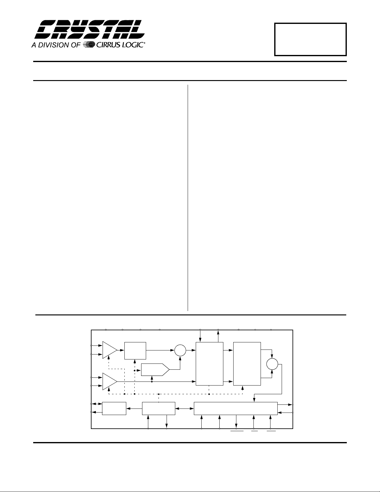
I
9$9$$*1'$*1'
;
;
%ULGJH
6\QF
*DLQ
%ORFN
$,1
$,1
95()
95()
%;
%;
Cirrus Logic, Inc.
Crystal Semiconductor Products Division
P.O. Box 17847, Austin, Texas 78760
(512) 445 7222 FAX: (512) 445 7581
http://www.crystal.com
ELW'$
&RQYHUWHU
&DOLEUDWLRQ
;,1;287
ORDERING INFORMATION
See page 29.
0'590'599'9''*1'
,1 287
Σ
&KDQQHO
'HOWD6LJPD
0RGXODWRU
,1 287
602'(6&/.'5'<&6567
Copyright Cirrus Logic, Inc. 1997
(All Rights Reserved)
&KDQQHO
),5
)LOWHU
6HULDO,QWHUIDFH
÷
62'
6,'
MAR ‘95
DS74F1
1
Page 2
CS5516
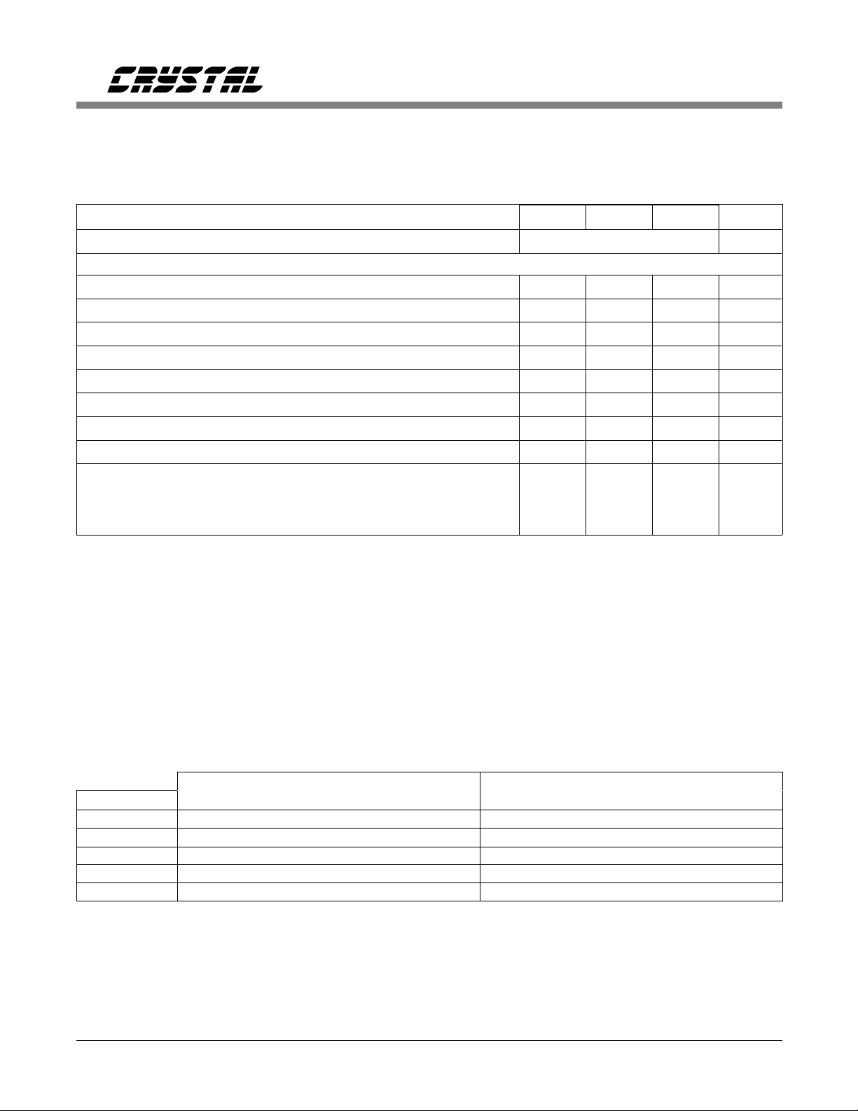
ANALOG CHARACTERISTICS (T
VREF= 2.5V (externa l differen tial volt age across VREF+ an d VREF-); f
AC Excitation 300 Hz; Gain = 25; Bipolar Mode; R
A
= T
source
MIN
to T
; VA+, VD+, MDRV+ = 5V; VA-, VD- = -5V;
MAX
= 4.9152 MHz ;
CLK
= 300Ω with a 4.7nF to AGND at AIN (see Note 1);
unless otherwise specified.)
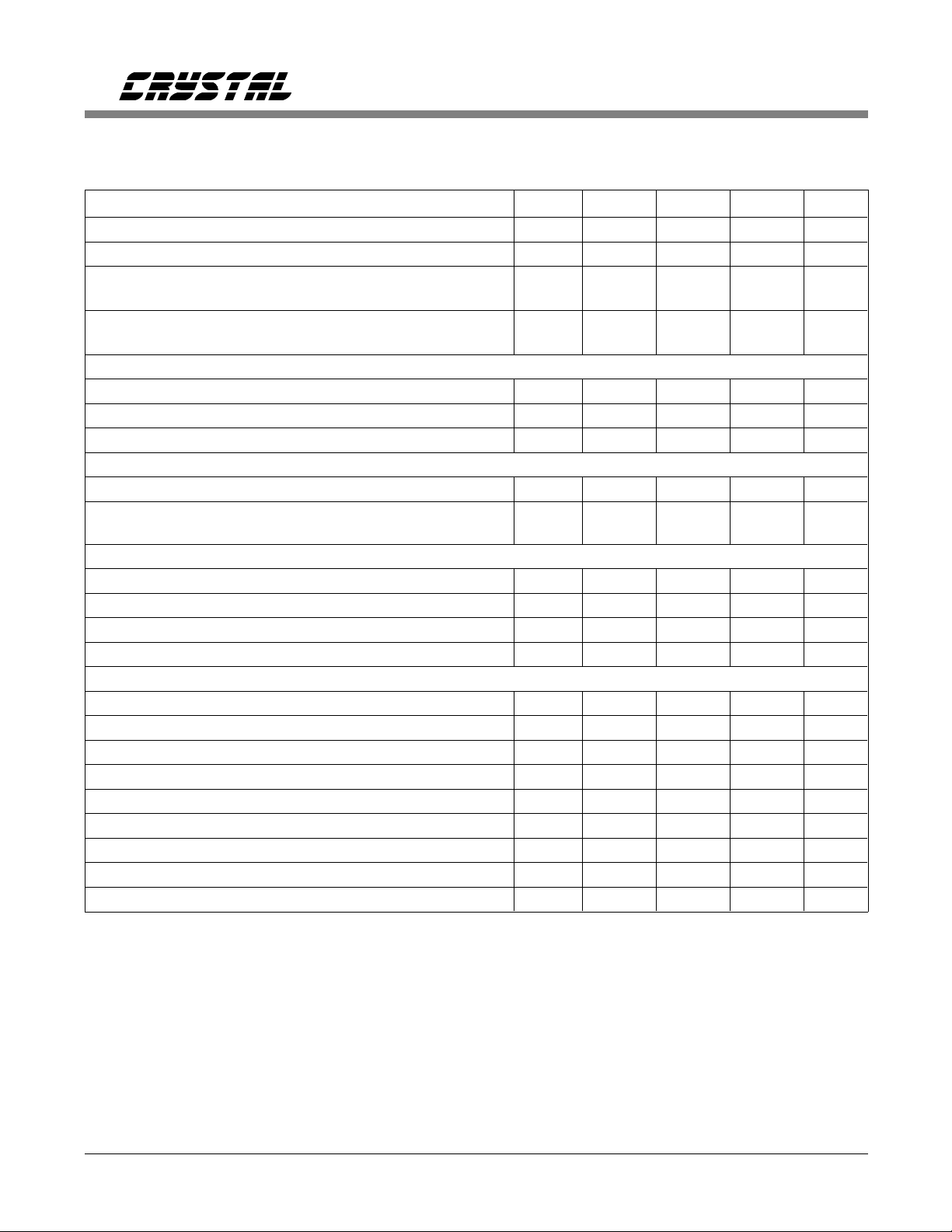
Parameter* Min Typ Max Units
Specified Temperature Range -40 to +85
°
C
Accuracy
Linearity Error - 0.0015 0.003
Differential Nonlinearity Unipolar Gain Error (Note 2) Bipolar Gain Error (Note 2) Unipolar/Bipolar Gain Drift Unipolar Offset (Note 2) Bipolar Offset (Note 2) Offset Drift Noise (Referred to Input) Gain = 25 (25 x 1)
Gain = 50 (25 x 2)
Gain = 100 (25 x 4)
Gain = 200 (25 x 8)
-
-
-
-
±
0.25
±
±
±
±
±
±
0.005
250
200
150
150
±
0.5
8
8
1
1
1
±
31
±
31
-
±
2
±
2
-
-
-
-
-
±
%FS
LSB
16
ppm
ppm
ppm/°C
LSB
16
LSB
16
µV/°
C
nVrms
nVrms
nVrms
nVrms
Notes: 1. The AIN and VREF pins present a very high input resistance at dc and a minor dynamic load which
scales to the master clock fr equency. Both source r esistance and shunt capac itance are therefore
critical in determining the source impedance requirements of the CS5516 and CS5520 at these pins.
2. Applies after system calibration at the temperature of interest.
Unipolar Mode Bipolar Mode
µ
V
LSB’s % FS ppm FS LSB’s % FS ppm FS
0.4 0.26 0.0004 4 0.13 0.0002 2
0.76 0.50 0.0008 8 0.26 0.0004 4
1.52 1.00 0.0015 15 0.50 0.0008 8
3.04 2.00 0.0030 30 1.00 0.0015 15
6.08 4.00 0.0061 61 2.00 0.0030 30
VREF = 2.5V PGA gain = 1
CS5516; 16-Bit Unit Conversion Factors
* Refer to the Specification Definitions immediately following the Pin Description Section.
Specifications are subject to change without notice.
2 DS74F1
Page 3
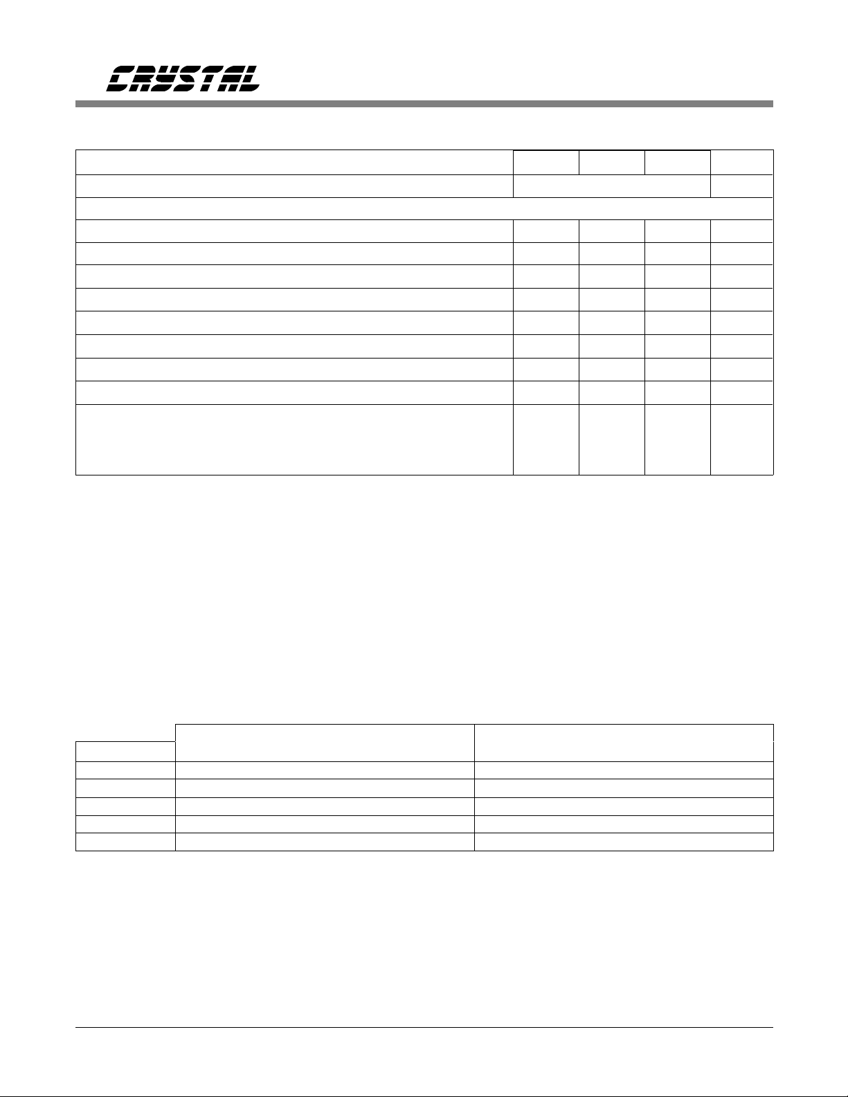
ANALOG CHARACTERISTICS (continued)
Parameter* Min Typ Max Units
CS5520
Specified Temperature Range -40 to +85
°
C
Accuracy
Linearity Error - 0.0007 0.0015
Differential Nonlinearity (No Missing Codes) 20 - - Bits
Unipolar Gain Error (Note 2) Bipolar Gain Error (Note 2) Unipolar/Bipolar Gain Drift Unipolar Offset (Note 2) Bipolar Offset (Note 2) Offset Drift Noise (Referred to Input) Gain = 25 (25 x 1)
Gain = 50 (25 x 2)
Gain = 100 (25 x 4)
Gain = 200 (25 x 8)
-
-
-
-
±
±
±
±
±
±
0.005
250
200
150
150
4
4
1
4
4
±
24
±
24
-
±
8
±
8
-
-
-
-
-
±
%FS
ppm
ppm
ppm/°C
LSB
LSB
µV/°
nVrms
nVrms
nVrms
nVrms
20
20
C
Unipolar Mode Bipolar Mode
µ
V
0.025 0.26 0.0000238 0.25 0.13 0.0000119 0.125
0.047 0.50 0.0000477 0.50 0.26 0.0000238 0.25
0.095 1.00 0.0000954 1.0 0.50 0.0000477 0.50
0.190 2.00 0.0001907 2.0 1.00 0.0000954 1.0
0.380 4.00 0.0003814 4.0 2.00 0.0001907 2.0
* Refer to the Specification Definitions immediately following the Pin Description Section.
DS74F1 3
LSB’s % FS ppm FS LSB’s % FS ppm FS
VREF = 2.5V PGA gain = 1
CS5520; 20-Bit Unit Conversion Factors
Specifications are subject to change without notice.
Page 4
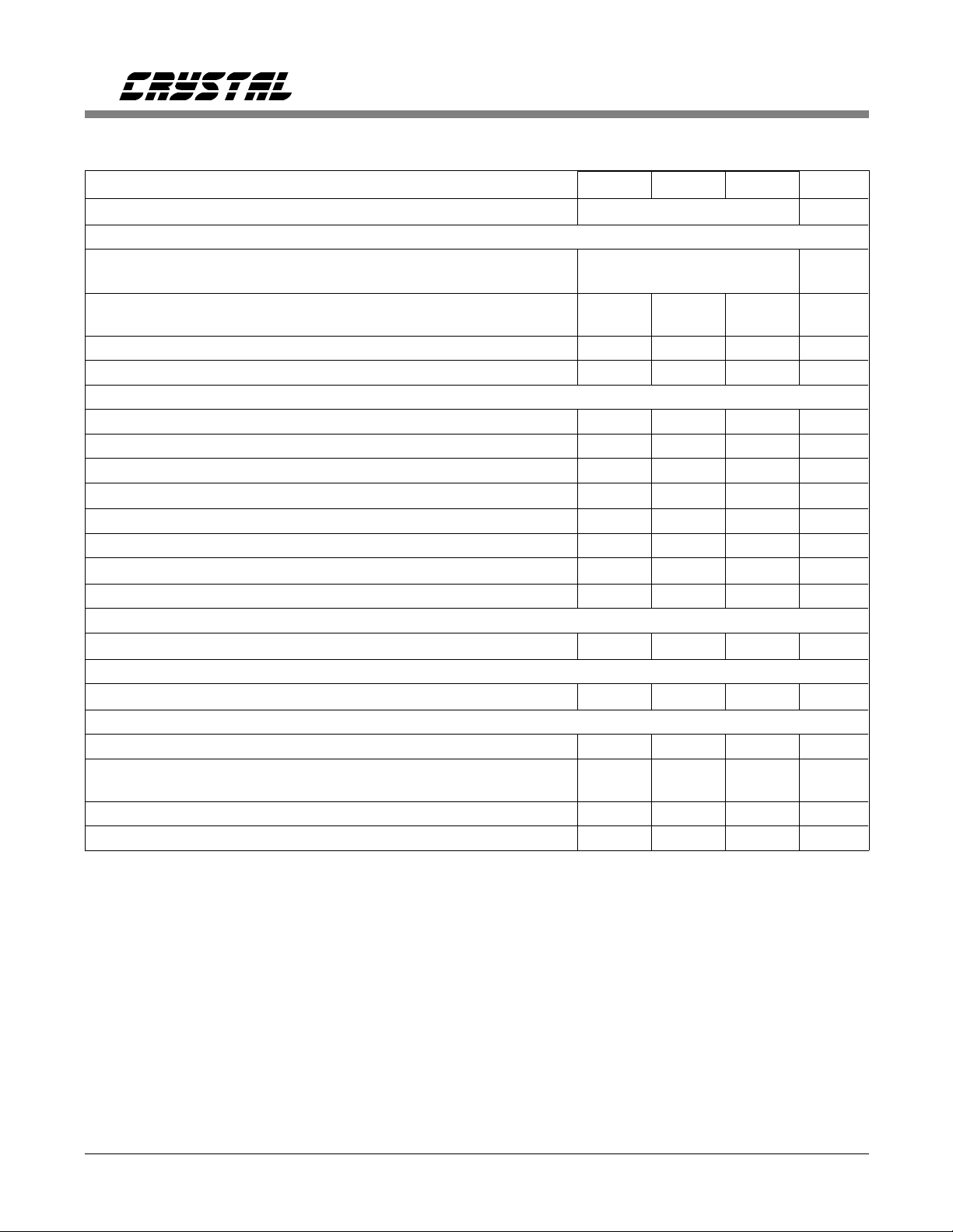
ANALOG CHARACTERISTICS (continued)
Parameter Min Typ Max Units
CS5516, CS5520
Specified Temperature Range -40 to +85
°
C
Analog Input
Analog Input Range Unipolar
Bipolar
Common Mode Rejection dc
50, 60 Hz
Input Capacitance - 5 - pF
Input Bias Current (Note 1) - 100 - pA
12.5, 25, 50, 100
±
12.5, ±25, ±50, ±100
-
-
165
200
mV
mV
-
-
dB
dB
Instrumentation Amplifier
Gain - 25 Bandwidth - 200 - kHz
Unity Gain Bandwidth - 5 - MHz
Output Slew Rate - 1.5 -
Noise @ 10 Hz BW - 100 - nV rms
Power Supply Rejection @ 50/60 Hz (Note 3) - 120 - dB
Common Mode Range (Note 4) -
Chopping Frequency - XIN/128 - Hz
±
3
-V
V/µsec
Programmable Gain Amplifier
Gain Tracking (Note 5) -
±
1
-%
4-Bit Offset Trim DAC
Accuracy -
±
5
-%
Voltage Reference Input
Range (Note 6) 2.0 2.5 3.8 V
Common Mode Rejection: dc
50, 60 Hz
Input Capacitance - 15 - pF
Input Bias Current (Note 1) - 10 - nA
Notes: 3. This includes the on-chip digital filtering.
4. The maximum magnitude of the differential input voltage, Vdiff(in) is determined by the following:
Vdiff(in) < 300 mV - |Vcm/12.5 | and should never exceed 300mV .
Vcm is the common mode voltage which is applied to the ins trumentation amplifier inputs.
The above equation should be used to calculate the allowable common mode voltage for a given
differential voltage applied to the firs t gain stage inputs. This limit ensures
that the instrumentation amplifier does not saturate.
5. Gain tracking accuracy can be significantly improved by uploading a calibrated gain word to the
gain register for each PGA gain s election.
6. The common mode voltage on the Voltage Reference Input, plus the reference range,
[(VREF+) - (VREF-)]/2, must not exceed ±3 volts.
-
-
60
200
-
-
dB
4 DS74F1
Page 5
CS5516, CS5520
ANALOG CHARACTERISTICS (continued)
Parameter Min Typ Max Units
Modulator Differential Voltage Reference
Nominal Output Voltage - 3.75 - V
Initial Output Voltage Tolerance -
Temperature Coefficient - 100 Line Regulation (4.75V < VA < 5.25V) - 0.5 - mV/V
Output Voltage Noise 0.1 to 15 Hz - 10 Output Current Drive: Source Current
Sink Current
-
-
±
100
-
-
Power Supplies
DC Power Supply Currents I
Power Dissipation: (Note 7)
Normal Operation
Standby Mode
Power Supply Rejection: dc Positive Supplies
dc Negative Supplies
I
A+
I
A-
D+
I
D-
-
-
-
-
-
-
-
-
2.7
-2.7
1.5
-0.6
37.5
10
100
95
System Calibration Specifications
Positive Full Scale Calibration Range (Note 8)
Unipolar Mode
Bipolar Mode
Maximum Ratiometric Offset Calibration Range (Note 8)
Unipolar Mode
Bipolar Mode
Differential Input Voltage Range (Notes 4, 8, 9, 10)
Unipolar Mode
Bipolar
Notes: 7. All outputs unloaded. All inputs CMOS levels.
8. T=VREF/(Gx25), where T is the full s cale span, where VREF i s the differential voltage ac ross
VREF+ and VREF- in volts, and G is the gain setting of the second gain block. G can be set
to 1, 2, 4, 8. This sets the overall gain to 25, 50, 100, 200. The gai n can then be fine tuned by
using the calibration of the full s cale point.
9. When calibrated.
10. V
is the offset corrected by the offset c alibration routine. V
offset
0.8T
0.8T
-2T
-2T
Voffset + (1.2T)
Voffset ± (1.2T)
offset
-
-
-
-
may be as large as 2T.
-mV
ppm/°C
µ
V
20
20
3.5
-3.5
2.2
-0.8
-
-
-
-
1.2T
1.2T
+2T
+2T
µ
µ
mA
mA
mA
mA
mW
µ
W
dB
dB
V
V
V
V
V
V
p-p
A
A
DS74F1 5
Page 6
DYNAMIC CHARACTERISTICS
Parameter Symbol Ratio Units
CS5516, CS5520
AIN and VREF Input Sampling Frequency f
Modulator Sampling Frequency f
Output Update Rate f
Filter Corner Frequency f
Settling Time to ±0.0007% (FS Step)
DIGITAL CHARACTERISTICS (T
= T
A
MIN
to T
MAX
is
s
out
-3dB
t
s
; VA+, VD+ = 5V ± 5%; VA-, VD- = -5V ± 5%;
DGND = 0) All measurements below are per formed under static conditions .
Parameter Symbol Min Typ Max Units
High-Level Input Voltage: XIN
All Pins Except XIN
Low-Level Input Voltage XIN
All Pins Except XIN
High-Level Output Voltage (Note 11) V
Low-Level Output Voltage l
= 1.6mA V
out
Input Leakage Current l
3-State Leakage Current l
Digital Output Pin Capacitance C
Notes: 11. I
= -100 µA. This guarantees the ability to drive one TTL load. (VOH = 2.4V @ I
out
V
V
V
V
IH
IH
IL
IL
(VD+)-1.0 - - V
OH
OL
in
OZ
out
f
/128 Hz
clk
f
/256 Hz
clk
f
/81,920 Hz
clk
f
/341,334 Hz
clk
4.5
2.0
-
-
6/f
out
-
-
-
-
-
-
0.5
0.8
s
V
V
V
V
--0.4V
-110
--
±
10
µ
A
µ
A
-9-pF
= -40 µA).
out
6 DS74F1
Page 7
CS5516, CS5520
RECOMMENDED OPERATING CONDITIONS (AGND, DGND = 0V, see Note 12.)
Parameter Symbol Min Typ Max Units
DC Power Supplies: Positive Digital
Negative Digital
Positive Analog
Negative Analog
Differential Analog Reference Voltage (VREF+) - (VREF-) 2.0 2.5 3.8 V
Analog Input Voltage: (Note 13)
Unipolar
Bipolar
Notes: 12. All voltages with respect to ground.
13. The CS5516 and CS5520 can accept input voltages up to +T in unipolar mode and -T to +T in bipolar
mode where T=VREF/(Gx25). G is the gain setting at the second gain block . When the inputs exceed
these values, the CS5516 and CS5520 will output positive full scale for any input abov e T, and
negative full scale for inputs below AGND in unipolar and -T in bipolar mode. This applies when the
analog input does not exceed ±2T overrange.
VD+
VD-
VA+
VA-
VAIN
VAIN
4.5
-4.5
4.5
-4.5
0
-T
5.0
-5.0
5.0
-5.0
-
-
5.5
-5.5
5.5
-5.5
+T
+T
V
V
V
V
V
V
ABSOLUTE MAXIMUM RATINGS* (AGND, DGND = 0V, all voltages with respect to ground.)
Parameter Symbol Min Typ Max Units
DC Power Supplies: Positive Digital (Note 14)
Negative Digital
Positive Analog
Negative Analog
Input Current, Any Pin Except Supplies (Notes 15, 16) l
Analog Input Voltage AIN and VREF pins V
Digital Input Voltage V
Ambient Operating Temperature T
Storage Temperature T
Notes: 14. No pin should go more positive than ( VA+)+0.3V. VD+ must always be less than (VA+)+0.3 V,and
can never exceed 6.0V.
15. Applies to all pins inc luding continuous overvoltage condi tions at the analog input pi ns.
16. Transient currents of up to 100mA will not cause SCR latch-up. Max imum input current for a power
supply pin is ± 50 mA.
* WARNING: Operation beyond these limits may r esult in permanent damage to the device.
Normal operation is not guaranteed at these extremes.
VD+
VD-
VA+
VA-
in
INA
IND
A
stg
-0.3
-0.3
-0.3
+0.3
--
(VA-)-0.3 - (VA+)+0.3 V
-0.3 - (VD+)+0.3 V
-55 - 125
-65 - 150
-
-
-
-
(VA+)+0.3
-5.5
5.5
-5.5
±
10
mA
°
°
V
V
V
V
C
C
DS74F1 7
Page 8
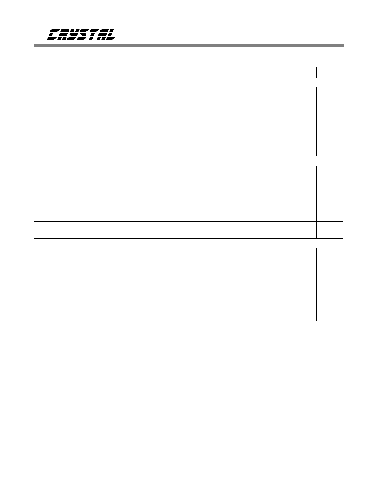
CS
CS5516, CS5520
SID
SCLK
DRDY
CS
SOD
SCLK
MSB
t
7
t
3
MSB-1
t
4
SID Write Timing (Not to Scale)
MSB MSB-1
t
6
t
5
t
1
t
2
LSB
t
8
t
1
t
2
t
9
DRDY
SOD
SCLK
CS
SCLK
SOD Read Timing (Not to Scale)
t
10
MSB MSB-1
t
8
SOD Read Timing with CS = 0 (Not to Scale)
t
12
t
13
CS with Continuous SCLK (Not to Scale)
t
1
LSB
t
9
t
2
t
14
t
15
8 DS74F1
Page 9
CS5516, CS5520
SWITCHING CHARACTERISTICS (T
VA-, VD- = -5V±5%; Input Levels: Logic 0 = 0V, Logic 1 = VD+; C
A
= T
MIN
to T
VA+, VD+ = 5V ± 5%;
MAX;
= 50 pF)
L
Parameter Symbol Min Typ Max Units
Master Clock Frequency: Internal Oscillator / External Clock XIN 1.0 4.096 5.0 MHz
Master Clock Duty Cycle 40 - 60 %
Rise Times Any Digital Input (Note 18)
Any Digital Output
Fall Times Any Digital Input (Note 18)
Any Digital Output
t
t
rise
fall
-
-
-
-
50
50
-
-
1.0
-
1.0
-
µ
ns
µ
ns
Startup
Power-on Reset Period t
Oscillator Start-up Time X TAL = 4.9152 MHz(Note 19) t
RST Pulse Width t
por
ost
res
- 100 - ms
-60-ms
1/XIN - - ns
Serial Port Timing
Serial Clock Frequency SCLK - - 2.4 MHz
Serial Clock Pulse Width High
Pulse Width Low
t
1
t
2
200
200
-
-
-
-
ns
ns
SID Write Timing
CS Enable to Valid Latch Clock t
Data Set-up Time prior to SCLK rising t
Data Hold Time After SCLK Rising t
SCLK Falling Prior to CS Disable t
3
4
5
6
150 - - ns
50 - - ns
50 - - ns
50 - - ns
SOD Read Timing
CS to Data Valid t
SCLK Falling to New Data Bit t
SCLK Falling to SOD Hi-Z t
DRDY Falling to Valid Data (CS = 0) t
CS Rising to SOD Hi-Z t
CS Disable Hold Time t
CS Enable Set-up Time t
CS Enable Hold Time t
CS Disable Set-up Time t
7
8
9
10
11
12
13
14
15
- - 150 ns
- - 170 ns
- - 200 ns
- - 150 ns
- - 150 ns
50 - - ns
150 - - ns
50 - - ns
150 - - ns
Notes: 18. Specified using 10% and 90% points on waveform of interest. Output loaded wi th 50 pF.
19. Oscillator start-up time var ies with crystal par ameters. This specification does not apply when us ing
an external clock source.
s
s
DS74F1 9
Page 10
GENERAL DESCRIPTION
CS5516, CS5520
The CS5516 and CS5520 are monolithic CMOS
A/D converters which include an instrumentation
amplifier input, an on-chip programmable gain
amplifier, and a DAC for offset trimming.
While the devices are optimized for ratiometric
measurement of Wheatstone bridge applications,
they can be used for general purpose low-level
signal measurement.
Each of the devices includes a two-channel differential delta-sigma modulator (the signal
measurement input and the reference input are
digitized independently before a digital output
word is computed), a calibration microcontroller,
a two-channel digital filter, a programmable instrumentation amplifier block, a 4-bit DAC for
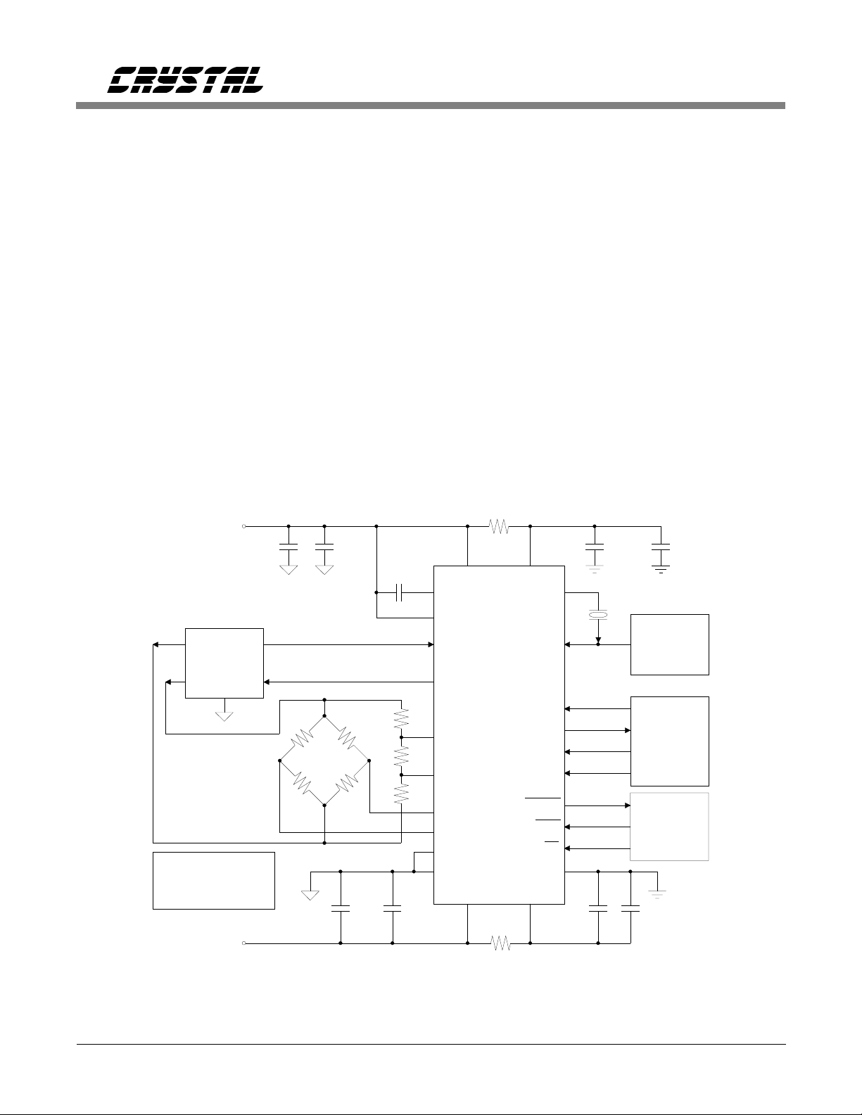
+5V
Analog
Supply
Bridge
Excitation
Supply
-
Unused logic inputs
must be connected
to DGND or VD+
-5V
Analog
Supply
0.1 µF1 µF1
1 µF
Excitation Supply
Synch. Signals
+
0.1 µF
1 µF 1 µF
coarse offset trimming, circuitry for generation
and demodulation of AC (actually switched DC)
bridge excitation, and a serial port. The CS5516
outputs 16-bit words; the CS5520 outputs 20-bit
words.
The CS5516/20 devices can measure either
unipolar or bipolar signals. Self-calibration is
utilized to maximize performance of the measurement system. To better understand the
capabilities of the CS5516/20, it is helpful to examine some of the error sources in bridge
measurement systems.
10
Ω
µ
F
Optional
Clock
Source
Serial
Data
Interface
Control
Logic
0.1 µF
2
1
12
11
9
10
6
7
5
8
320
10
VD+
SMODE
DGND
VD-
Ω
VA+
MDRVMDRV+
BX1
BX2
VREF+
VREF-
AIN+
AINAGND1
AGND2
VA-
CS5516
CS5520
XOUT
XIN
SCLK
SOD
SID
DRDY
RST
CS
214
0.1 µF
23
22
16
18
17
24
15
13
14
19
Figure 1. System Connection Diagram: AC Excitation Mode Using External Excitation
10 DS74F1
Page 11
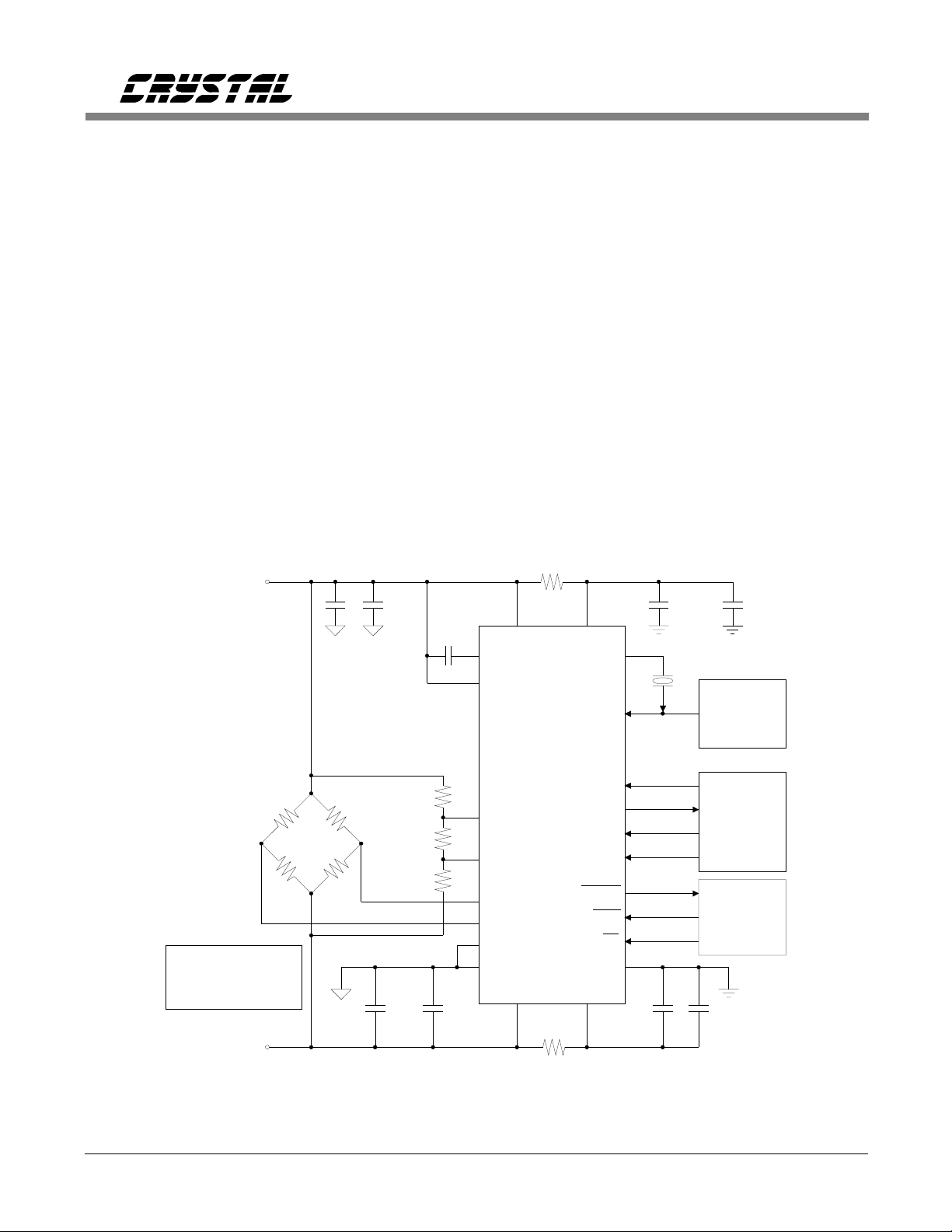
THEORY OF OPERATION
CS5516, CS5520
The front page of this data sheet illustrates the
block diagram of the CS5516 and CS5520 A/D
converter. The device includes an instrumentation amplifier with a fixed gain of 25. This
chopper-stabilized instrumentation amplifier is
followed by a programmable gain stage with
gain settings of 1, 2, 4, and 8. The sensitivity of
the input is a function of the programmable gain
setting and of the reference voltage connected
between the VREF+ and VREF- pins of the device. The full scale of the converter is VREF/( G
x 25) in unipolar, or ±VREF/(G x 25) in bipolar,
where VREF is the reference voltage between
the VREF+ and VREF- pins, G is the gain setting of the programmable gain amplifier, and 25
is the gain of the instrumentation amplifier.
+5V
Analog
Supply
-
Unused logic inputs
must be connected
to DGND or VD+
-5V
Analog
Supply
0.1 µF1 µF1
1 µF
+
0.1 µF
1 µF 1 µF
After the programmable gain block, the output
of a 4-bit DAC is combined with the input signal. The DAC can be used to add or subtract
offset from the analog input signal. Offsets as
large as ±200 % of full scale can be trimmed
from the input signal.
The CS5516 and CS5520 are optimized to perform ratiometric measurement of bridge-type
transducers. The devices support dc bridge excitation or two modes of ac (switched dc) bridge
excitation. In the switched-dc modes of operation the converter fully demodulates both the
reference voltage and the analog input signal
from the bridge.
10
Ω
µ
F
Optional
Clock
Source
Serial
Data
Interface
Control
Logic
2
1
9
10
6
7
5
8
320
10
VD+
SMODE
DGND
VD-
Ω
VA+
MDRVMDRV+
CS5516
CS5520
VREF+
VREF-
AIN+
AINAGND1
AGND2
VA-
XOUT
XIN
SCLK
SOD
SID
DRDY
RST
CS
214
0.1 µF
23
22
16
18
17
24
15
13
14
19
0.1 µF
Figure 2. System Connection Diagram: DC Excitation Mode (EXC bit = 0), F1 = F0 = 0.
DS74F1 11
Page 12

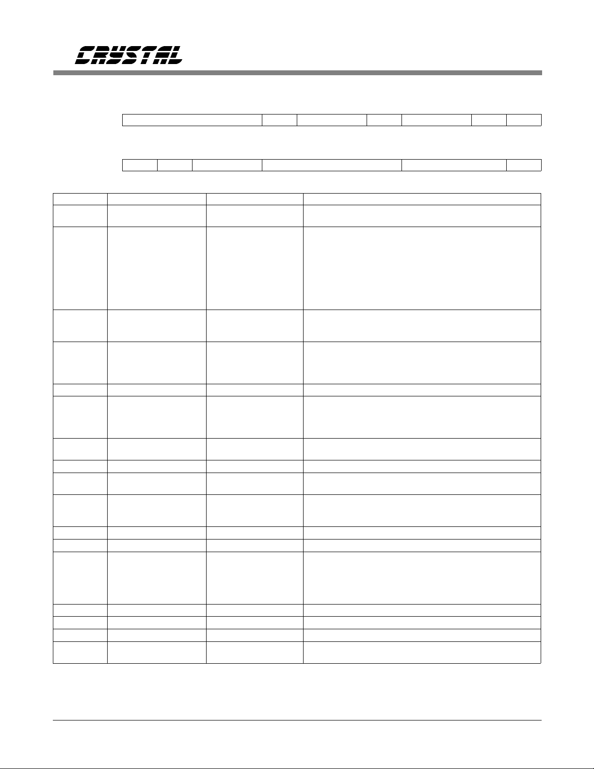
Command Register
D7 D6 D5 D4 D3 D2 D1 D0
1 RSB2 RSB1 RSB0 R/
BIT NAME VALUE FUNCTION
D7 D7 1 Must always be logic 1
RSB2-0 Register Select Bit
000
001
010
011
100
101
110
111
R/W R ead/Write 0
D2
D1
D0
D2
D1
D0
1
0
0
0
Selects Re gister to be Read o r Writte n per R/
CONVERSION DATA (read only )
CONFIGURATION
GAIN
DAC
RATIOMETRIC OFFSET
NON-RATIOMETRIC OFFSET - AIN
NON-RATIOMETRIC OFFSET - VREF
NOT USED
Write to the registe r selected by th e RSB2-0 bi ts
Read from the regi ster selec ted by the RS B2-0 bits
Not Used
Not Used
Not Used
W0 0 0
CS5516, CS5520
W bit
Table 1. CS5516 and CS5520 Commands
The CS5516/20 includes a microcontroller which
manages operation of the chip. Included in the
microcontroller are eight different registers associated with the operation of the device. An 8-bit
command register is used to interpret instructions received via the serial port. When power
is applied, and the device has been re set, the serial port is initialized into the command mode.
In this mode it is waiting to receive an 8-bit
command via its serial port. The first 8 bits into
the serial port are placed into the command register. Table 1 lists all the valid command words
for reading from or writing to internal registers
of the converter. Once a valid 8-bit command
word has been received and decoded, the serial
port goes into data mode. In data mode the next
24 serial clock pulses shift data either into or out
of the serial port. When writing data to the port,
the data may immediately follow the command
word. When reading data from the port, the user
must pause after clocking in the 8-bit command
word to allow the microcontroller time to decode
the command word, access the appropriate regis-
ter to be read, and present its 24-bit word to the
port. The microcontroller will signal when the
24-bit read data is available by causing the
DRDY pin to go low.
The user must write or read the full 24-bit word
except in the case of reading conversion data. In
read data conversion mode, the user may read
less than 24 bits if CS is then made inactive
(CS = 1). CS going inactive releases user control
over the port and allows new data updates to the
port.
The user can instruct the on-chip microcontroller
to perform certain operations via the configuration register. Whenever a new word is written
to the 24-bit configuration register, the microcontroller then decodes the word and executes
the configuration register instructions. Table 2
illustrates the bits of the configuration register.
The bits in the configuration register will be discussed in various sections of this data sheet.
12 DS74F1
Page 13
Configuration Register
D23 D22 D21 D20 D19 D18 D17 D16 D15 D14 D13 D12
Register
Reset (R)
Register
Reset (R)
DAC3 DAC2 DAC1 DAC0 EXC F1 F0 D16 G1 G0 U/B D12
000000000000
D11 D10 D9 D8 D7 D6 D5 D4 D3 D2 D1 D0
A/S EC D9 D8 CC3 CC2 CC1 CC0 D3 D2 D1 RF
000000000000
CS5516, CS5520
BIT NAME VALUE FUNCTION
DAC3 DAC Sign Bit 0
1
DAC2-0 DAC Bits 000
001
010
011
100
101
110
111
EXC E xcitatio n: Internal
External
F1-F0 Select Frequenc y 00
D16 D16 0
G1-G0 Select PGA Gain 00
U/B Select Unipolar/B ipo-
lar Mode
D12 D12 0
A/S Awake/ Sleep 0
EC Execute Cali bration 0
D9 D9 0
D8 D8 0
CC3-CC0 Calibration Control Bits 0000
D3 D3 0
D2 D2 0
D1 D2 0
RF Reset Filter 0
0
1
01
10
11
10
01
11
0
1
1
1
1000
0100
0010
0001
1
1
R
Add Offset
Subtract Offset This bit is read only
R
25% Offset
50% Offset
75% Offset
100% Offset These bits are read only
125% Offset
150% Offset
175% Offset
R
R
R
R
R
R
R
R
R
R
R
R
R
R
R
BX1 and BX2 outp uts are de termi ned by bits F1 and F0
BX1 is an input which determines the phase of the
demodulation clock and the BX2 output
Excitation on BX1 & BX2 is dc. BX1=0 V, BX2=+5 V
Excitation Frequency on BX1 & BX2 is XIN/8192 Hz
Excitation Frequency on BX1 & BX2 is XIN/16384 Hz
Excitation Frequency on BX1 & BX2 is XIN/4096 Hz
Must always be logic 0
Gain = 1 (X25)
Gain = 2 (X25)
Gain = 4 (X25)
Gain = 8 (X25)
Bipolar Measureme nt Mode
Unipolar Measurement Mode
Must always be logic 0
Awake Mode
Sleep Mode
Calibration not active
Perform calibratio n select ed by CC 3-CC0 bi ts. EC bi t
must be written back to "0" after calibration is completed
Must always be logic 0
Must always be logic 0
No calibration to be performed
Calibrate non-ratiometric offset, VREF
Calibrate non-ratiometric offset, AIN
Calibrate ratiometric offset, AIN
Calibrate gain, AIN
Must always be logic 0
Must always be logic 0
Must always be logic 0
Normal operation
Reset Filter
2
2
Notes:1.Reset State
2.A write to these bits does not change the register bit values. These bits are just a mirror of the DAC register contents.
Table 2. Configuration Register
DS74F1 13
Page 14

CS5516, CS5520
System Initialization
Whenever power is applied to the
CS5516/CS5520 A/D converters, the devices
must be reset to a known condition before
proper operation can occur. The internal reset is
applied after power is established and lasts for
approximately 100 ms. The RST pin can also be
used to establish a reset condition. The reset signal should remain low for at least one XIN clock
cycle to ensure adequate reset time. It is recommended that the RST pin be used to reset the
converter if the power supplies rise very slowly
or with poor startup characteristics. The RST
signal can be generated by a microcontroller output, or by use of an R-C circuit.
The reset function initializes the configuration
register and all five of the calibration registers;
and places the microcontroller in command
mode ready to accept a command from the serial
port. Whenever the device is reset the DRDY
pin will be set to a logic 1 and the on-chip registers are initia lized to t he following s tates:
Configuration 000000(H)
Calibration registers:
DAC 000000(H)
Gain 800000(H)
AIN Ratiometric Offset 000000(H)
AIN Non-ratiometric Offset 000000(H)
VREF Non-ratiometric Offset 000000(H)
CALIBRATION
After the CS5516/20 is reset, the device is functional and can perform measurements without
being calibrated. The converter will utilize the
initialized values of the calibration registers to
calculate output words.
The converter uses the two outputs (AIN &
VREF) of the dual channel converter along with
the contents of the calibration registers to compute the conversion data word. The following
equation indicates the computation.
D
− R1
R0 = R4 [[
Where R0 is the output data, D
D
VREF
AIN
− R2
] − R3]
and D
AIN
VREF
are the digital output words from the AIN and
VREF digital filter channels, and R1, R2, R3
and R4 are the contents of the following calibration registers:
R1 = AIN non-ratiometric offset
R2 = VREF non-ratiometric offset
R3 = AIN ratiometric offset
R4 = Gain
The computed output word, R0, is a two’s complement number.
Calibration minimizes the errors in the converted
output data. If calibration has not been performed, the measurements will include offset
and gain errors of the entire system.
The converter may be calibrated each time it is
powered up, or calibration words from a previous calibration may be uploaded into the
appropriate calibration registers from some type
of E2PROM by the system microcontroller.
The converter uses five different registers to
store specific calibration information. Each of
the calibration registers stores information pertinent to correcting a specific source of error
associated with either the converter or with the
input transducer and its wiring. The method by
14 DS74F1
Page 15

CS5516, CS5520
Configuration Register
EC CC3 CC2 CC1 CC0
11000 VREF Non-ratiometric Offset 573,440/fclk
10100 AIN Non-ratiometric Offset 573,440/fclk
10010 AIN Ratiometric Offset 2,211,840/fclk
10001 AIN System Gain 573,440/fclk
11100VREF & AIN Non-ratiometric Offset 573,440/fclk
0XXXX End Calibration -
DRDY remains high through calibration sequence. In all modes, DRDY falls immediately upon completion of the calibration
sequence.
Table 3. CS5516/CS5520 Calibration Control
which calibration is initiated is common to each
of the calibration registers. The configuration
register controls the execution of the calibration
process. Bits CC3--CC0 in the configuration
register determine which type of calibration will
be performed and which of the five calibration
registers will be affected. On the falling edge of
the 24th SCLK, the configuration word will be
latched into the configuration register and the se-
formed. The calibration steps should be performed in the following sequence. If the user
determines that non-ratiometric offset calibration is important, the non-ratiometric offset
errors of the VREF and AIN input channels
should be calibrated first. Then the ratiometric
offset of the AIN channel should be calibrated.
And finally, the AIN channel gain should be
calibrated.
CAL Type Calibration Time
lected calibration will be executed. The time
required to perform a calibration is listed in Table 3. The DRDY pin will remain a logic 1
during calibration, and will go low when the
calibration step is completed.
The serial port should not be accessed while a
calibration is in progress. The EC bit of the
configuration register remains a logic 1 until it is
overwritten by a new configuration word (EC =
0). Consequently, if EC is left active, any write
(the falling edge of the 24th SCLK) to any register inside the converter will cause a re-execution
of the calibration sequence. This occurs because
the internal microcontroller executes the contents
of the configuration register every time the 24th
SCLK falls after writing a 24-bit word to any
internal register. To be certain that calibrations
will not be re-executed each time a new word is
written or read via the serial port, the EC bit of
Non-ratiometric Errors
To calibrate out the VREF and AIN
non-ratiometric errors, the input channels to the
VREF path into the converter and the AIN path
into the converter must be grounded (this may
occur at the pins of the IC, or at the bridge excitation as shown in Figure 3.). Then the EC,
CC2 and CC3 bits of the configuration register
must be set to logic 1. The converter will then
perform a non-ratiometric calibration and place
BX1
BX2
CS5516
CS5520
VREF+
VREF-
AIN+
+
1A*1B*
-
the configuration register must be written back
to a logic 0 after the final calibration step has
been completed.
The CC3--CC0 bits of the configuration register
determine the type of calibration to be per-
*Note: The bridge can be grounded with a
Figure 3. Non-ratiometric System Calibration using
AIN-
relay or with jumpers to perform
non-ratiometric calibration.
Internal Excitation
DS74F1 15
Page 16

CS5516, CS5520
the proper 24 bit calibration words in the VREF
and AIN non-ratiometric registers. Note that the
two non-ratiometric offsets can be calibrated simultaneously or independently, but they must be
calibrated prior to the other calibration steps if
non-ratiometric offset calibration is to be used. If
the effects of the non-ratiometric errors are not
significant enough to affect the user application,
they can be left uncalibrated (after a reset, the
non-ratiometric offset registers will contain
000000(H)).
Ratiometric Offset
Once the non-ratiometric errors have been calibrated, the ratiometric offset error of the AIN
channel should be calibrated next. To perform
this calibration step, a reference voltage must be
applied to the VREF+ and VREF- pins. Then,
place "zero" weight on the scale platform. This
will result in an offset voltage into the converter
which will represent the offset of the bridge, the
wiring, and the AIN input of the converter itself.
A configuration word with the EC and CC1 bits
set to logic 1 is then written into the configuration register. During the ratiometric offset
calibration of AIN the microcontroller first uses
a successive approximation algorithm to compute the correct values for the DAC3-DAC0 bits
of the DAC register. This accommodates any
large offsets on the AIN input signal. Once the
four DAC bits are computed, this amount of offset is removed from the input signal. The
microcontroller then computes the appropriate
24 bit number to place in the AIN ratiometric
offset register to calibrate out the remaining offset not removed by the DAC.
Gain
After the AIN ratiometric offset has been calibrated, the next step is to perform a gain
calibration. Gain calibration is performed with
"full scale" weight on the scale platform. The
EC and CC0 bits of the configuration register
are set to logic 1. The gain calibration of the
AIN channel is the final calibration step. After
DRDY falls to signal the completion of this calibration step, the EC bit of the configuration
register must be set back to logic 0 to terminate
the calibration mode.
Limitation s in Calib ration Range
There are five calibration registers in the converter. There are two non-ratiometric offset
calibration registers, one for the AIN input and
one for the VREF input; one 4-bit offset trim
DAC; one ratiometric offset calibration register
for the AIN input; and one gain calibration register. After the non-ratiometric offsets are
calibrated, an LSB in either of the 24-bit non-ratiometric calibration registers represents 2
-23
proportion of an internally-scaled MDRV
(Modulator Differential Reference Voltage). At
the MDRV+ and MDRV- pins, the MDRV has a
nominal value of 3.75 volts. This voltage is internally scaled to a nominal 2.5 volts (never less
than 2.4 volts) for use with the non-ratiometric
calibration. The two non-ratiometric calibration
words are stored in 2’s complement form with
one count equal to slightly less than 300 nV at
the input of the internal A/D converter. For the
AIN channel this will be scaled down by the
gain of the instrumentation amplifier (X25) and
the PGA gain. For a PGA gain = 1, one count of
a non-ratiometric register will represent slightly
less than 12 nV. Non-ratiometric offset at the
VREF input cannot exceed ± 2.4 volts to be
within calibration range of the converter. Nonratiometric offset to be calibrated by the AIN
channel cannot exceed ± 2.4 volts divided by the
channel gain. With a PGA gain = 1, the maximum non-ratiometric offset which can be
calibrated on the AIN channel cannot exceed
± 96 mV.
When the ratiometric offset is calibrated, the 4bit DAC coarsely trims offset from the analog
signal. The ratiometric offset which remains is
finely trimmed after the signal has been converted; using the contents of the ratiometric
offset register for digital correction. The DAC
16 DS74F1
Page 17

CS5516, CS5520
bits can be manipulated by the user to add or
subtract offset up to 200 percent of the nominal
input signal. The AIN ratiometric offset register
can be manipulated to add or subtract offset
equal to the maximum differential input signal
into the X2 5 amplifier. An LSB in the ra tiometric offset register represents 2
-23
proportion of
the voltage input across the VREF+ and VREFpins at the internal input to the AIN channel
A/D converter. This will be scaled down by the
AIN channel gain when calculated relative to the
instrumentation amplifier input. For example,
with a VREF = 2.5 V, the PGA gain = 1, one
count of the ratiometric offset register would
represent about 12 nV at the instrumentation amplifier input. The proportion remains ratiometric
even if the VREF voltage should change. The
24-bit register content is stored in 2’s complement form.
Manipulation of the DAC or ratiometric offset
register allows the user to shift the transfer function to allow for load cell creep or load cell zero
drift.
The gain calibration is performed last. The contents of the gain register spans from 2
-23
to 2 as
shown in Table 4. After gain calibration has
been performed, the numeric value in the gain
register should not exceed the range of 0.8 to
1.2. The gain calibration range is ± 20 % of the
nominal value of 1.0. The nominal value of 1.0
is for an input span dictated by the VREF voltage, the PGA gain, and the X25 instrumentation
gain. The converter may operate with gain slope
factors from 0.5 to 2.0 (decimal), but when the
slope exceeds 1.2 the converter output code
computation may lack adequate resolution and
result in missing codes in the transfer function.
Internal circuitry may saturate for large signals
which would calibrate to a gain factor less than
0.8.
In a typical weigh scale application, the
CS5516/CS5520 will be calibrated in combination with a load cell at the factory. Once
calibrated, the calibration words are off-loaded
from the converter and stored in E2PROM.
When powered-up in the field the calibration
words are up-loaded into the appropriate registers. This is viable because the AIN and VREF
input to the converter are "chopper-stabilized"
and maintain excellent stability when subjected
to changes in temperature.
Programmable Gain Amplifier
The programmable gain amplifier inside the
CS5516/20 offers gains of 1, 2, 4, and 8. This is
in addition to the fixed gain of × 25 in the input
instrumentation amplifier. The gain tracking of
the PGA is about one percent between ranges.
The user can remove this error by performing a
gain calibration at the factory with a full scale
signal on each range. The gain calibration word
for each gain range can be off-loaded into
E2PROM and uploaded into the gain register
whenever a new gain setting is selected for the
PGA. Gain stability over temperature for the
converter itself is approximately 1 ppm/°C when
the device is used ratiometrically.
Serial Interface Modes
The CS5516/20 support either 5, 4 or 3 pin serial interfacing. The SMODE pin sets the
operating mode of the serial interface. With
SMODE = 0, the device assumes the user is operating with either a 5 or 4 wire interface. The
five wire mode includes SOD, SID, SCLK,
DRDY, and CS. In the four wire mode, CS is
connected to DGND as a logic 0. The user
would then interface to the SOD, SID, SCLK,
and DRDY pins.
DS74F1 17
Page 18

AIN and VREF Non-Ratiometric Offset Registers
MSB LSB
Register
Reset (R)
0
2
000000 000000
-1
2
-2
2
-3
2
-4
2
-5
2
-18
2
≈
CS5516, CS5520
-19
2
-20
2
-21
2
-22
2
-23
2
One LSB represents 2
-23
proportion of th e internal MDRV (≈2.5 Volts)
DAC Register
D23 D22 D21 D20 D19 D18 D17 D16 D15 D14 D13 D12
Register
Reset (R)
Register
Reset (R)
BIT NAME VALUE FUNCTION
DAC3 DAC Sign Bit 0
DAC2-0 DAC Bits 000
Bits
D19 to D0
DAC3 DAC2 DAC1 DAC0 EXC F1 F0 D16 G1 G0 U/B D12
000000000000
D11 D10 D9 D8 D7 D6 D5 D4 D3 D2 D1 D0
A/S EC D9 D8 CC3 CC2 CC1 CC0 D3 D2 D1 RF
000000000000
1
1
R
Add Offset
Subtract Offset
R
001
010
011
100
101
110
111
0
R
25% Offset
50% Offset
75% Offset
100% Offset
125% Offset
150% Offset
175% Offset
These bits mi rror t he
Configuration Register
read only
2
Note: 1. Reset State
2. A write to these bi ts does not ch ange the regis ter bit valu es.
AIN Ratiometric Offset Register
MSB LSB
Register
Reset (R)
One LSB represents 2
0
2
000000 000000
-1
2
-2
2
-3
2
-4
2
-5
2
-18
2
-19
2
-20
2
-21
2
≈
-23
proportion of the voltage [<(VREF+) - (VREF-)>/GAIN] where GAIN = 25 X PGA Gain
-22
2
-23
2
GAIN Register
MSB LSB
Register
Reset (R)
The gain reg ister span f rom 0 t o (2-2
0
2
100000 000000
18 DS74F1
-1
2
-2
2
-3
2
-4
2
-5
2
-18
2
-19
2
-20
2
-21
2
-22
2
-23
2
≈
-23
). After Reset the MSB=1, all other bits are 0.
Table 4. Calibration Registers
Page 19

CS5516, CS5520
Reading a register in the converter requires a
command word to be written to the SID pin.
For example, to read the conversion data register, the following command sequence should be
performed. First, the command word 88(H)
would be issued to the port. In the 5 wire interface mode, this would involve activating CS
low, followed by 8 SCLKs (note that SCLK
must always start low and transition from low to
high to latch the transmit data, and then back
low again) to input the 8-bit command word. CS
must be low for the serial port to recognize
SCLKs during a write or a read, but it is actually
the first rising SCLK during command time that
gives the user control over the port. After writing the command word, the user must pause and
wait until the CS5520 presents the selected register data to the serial port. The DRDY signal
will fall when the data is available. When reading the conversion data register, it may take up
to 112,000 XIN clock cycles for DRDY to fall
after the 88(H) command word is recognized.
See Figure 4 for an illustration of command and
data word ti ming.
The conversion data register is actually the accumulator of the post-processor which computes
the output data. At the end of each filter convolution cycle, the internal microcontroller checks
to see if a read conversion data register command has been interpreted. If so, it transfers the
accumulator result to the serial port.
Whenever registers other than the conversion
data register are read, the DRDY pin will fall
within 256 XIN clock cycles (62.5 µs with
XIN = 4.096 MHz) after the command word is
recognized. When DRDY falls, 24 SCLKs are
then issued to the port to read the 24-bit output
data word. DRDY will return high after all 24
bits have been clocked out. The SOD pin will be
in a Hi-Z state whenever CS is high, or after all
24 output data bits have been clocked out of the
port.
The CS5516/20 is designed such that it can output conversion data words continuously, without
issuing a new command word prior to each data
read. Under the following circumstances, continuous conversion data can be read from the
port after issuing only one 88(H) command
word. Once the command to read the conversion
data register is issued, DRDY must be allowed
to go low, after which 24 SCLKs are issued to
read the data. This will cause DRDY to return
high.
The converter will continue to output conversion
words at the update rate as long as a different
command word is not started prior to DRDY
falling again. The user is not required to read
every output word to remain in the continuous
update mode. DRDY will toggle high, and then
low as each new output word becomes available.
If a command word is issued immediately after a
data word is read, the converter will end the read
conversion mode. Figure 5 illustrates the continuous data mode.
The user should perform all data reads and command writes within 51,000 XIN clock cycles
after DRDY falls to avoid ambiguity as to who
controls the serial port.
If SMODE = 1 (tied to VD+), the interface operates as a 3 wire interface using only SOD, SID,
and SCLK. In the 3 wire mode CS must be tied
to DGND. DRDY operates normally but is not
used. Instead, the DRDY signal modifies the
behavior of the SOD signal, allowing it to signal
to the user when data is available. To read data
from the converter requires a command word to
be written to the SID pin. The SOD output is
normally high (never Hi-Z). When output data
is available, the SOD signal will go low. The
user would then issue 8 SCLKs to the SCLK pin
to clear this data ready signal. On the falling
edge of the 8th SCLK the SOD pin will present
the first bit of the 24-bit output word. 24 SCLKs
are then issued to read the data. Then SOD will
go high. SID should remain low whenever the
DS74F1 19
Page 20

CS
SCLK
CS5516, CS5520
SID
CS
SCLK
SID
DRDY
SOD
Command Time
8 SCLKs
Command Time
8 SCLKs
MSB
SID Write
t *
d
MSB
SOD Read (4 or 5 Wire)
LSB
Data Time
24 SCLKs
LSB
Data Time
24 SCLKs
SCLK
SID
81,920 XIN
Clock Cycles
LSB
SOD falls if
Command
was 88(H)
SOD
Command Time
8 SCLKs
t *
d
8 SCLKs Clear DRDY
SOD Read (3 Wire)
MSB
Data Time
24 SCLKs
Figure 4. Command and Data Word Timing
*See text for t
time.
d
20 DS74F1
Page 21

CS5516, CS5520
SID pin is not being written. When reading
SOD, SCLK cannot be continuous but must
burst one clock cycle per bit.
The continuous read conversion data mode is
also functional in the 3-wire interface mode. Issue one 88(H) command word to the converter.
Then wait for SOD to go low. Issue 8 SCLKs to
clear the data ready function. The MSB data bit
will then appear on the SOD pin. Issue 24
SCLKs to read the conversion word. At the falling edge of the 24th SCLK SOD will return
high. SOD will go low at the next DRDY falling
time to indicate a new conversion word. Eight
SCLKs must again be issued to clear the data
ready function before clocking out the data conversion word. The SOD pin will continue to
toggle low each time a word is available even if
the conversion data is not read. To terminate the
continuous conversion mode, input an 8-bit command word immediately after reading a
conversion word.
The user should perform all data reads and command writes within 51,000 XIN clock cycles
after SOD falls to avoid ambiguity as to who
controls the serial port.
Serial Port Initialization
If for any reason the off-chip microcontroller
fails to know whether the serial port of the
CS5516/20 is in data mode or command mode,
the following initialization procedure can be issued to the port to force the CS5516/20 into the
command mode. Write 128 or more 1’s to the
SID pin. Then issue a single 0 to the SID pin.
The port will then be initialized into the command mode and will be waiting for an 8-bit
command word.
Bridge Excitation Options
The CS5516/CS5520 A/D converters are optimized for Wheatstone bridge applications. The
converters support either dc or ac (switched dc)
bridge excitation.
DC Bridge Excitation
The CS5516/CS5520 can be configured for dc
bridge excitation in either of two ways. The
EXC bit of the configuration register can be set
for either internal or for external excitation. If
set to internally-controlled mode (EXC = 0), the
F1 and F0 bits must be set to logic 0s. In this
condition, the bridge can be excited from a dc
supply with a resistor divider to develop the appropriate reference voltage for the VREF+ and
VREF- pins. Note that the bridge excitation
Port Access Period
Valid 51,000
XIN Clock Cycles
CS
SCLK
8 SCLKs 24 SCL Ks 24 SCLKs
SID
8 Data Bits
DRDY
SOD
Figure 5. Continuous Read Conversion Data Mode (4 or 5 Wire)
DS74F1 21
81,920 XIN
Clock Cycles
24 Data Bits
24 Data Bits
Page 22

CS5516, CS5520
should not be applied prior to the
CS5516/CS5520 being powered-up. With EXC,
F1, and F0 set to logic 0, the BX1 output will be
logic 0 (0 volts) and the BX2 output will be a
logic 1 (+5 volts).
A second method for configuring the converter
for dc excitation is by setting EXC = 1, and
pulling up BX1 (pin 12) to VD+ (pin 20)
through a resistor. This sets the converter for
use with external excitation which uses the
BX1 pin as an input to set the excitation frequency. With BX1 = VD+, the external
excitation frequency is zero, or dc.
AC Bridge Excitation
AC bridge excitation involves using a clock signal to generate a square wave which repetitively
reverses the excitation polarity on the bridge. To
excite the bridge dynamically requires some type
of bridge driver external to the CS5516/CS5520
converter. This driver is driven by a square wave
clock. The source of this clock depends upon
whether the converter is set for internal excitation or for external excitation. Figure 6
illustrates a sample bridge drive circuit when operating in the internal AC excitation mode.
+5V
+
-5V
EXC+
EXC-
10 µF0.1 µF
+5V
-5V
+5V
-5V
+5V
0V
100 k
BX2
TP0610
10 k
10 k
Figure 6. Sample AC Bridge Driver
2
4
-5V
6
7
5
MICREL
3
MIC4428 or
MIC4425
Using internal excitation involves setting the
EXC bit of the configuration register to 0, and
setting th e F1 and F 0 bits to sele ct the excitat ion
frequency for the bridge. In this mode the excitation frequency is a sub-multiple of the XIN
clock frequency. The excitation clock is output
from the BX1 and BX2 pins of the converter in
the form of a two-phase non-overlapping clock.
The converter is capable of demodulating this
clocked excitation. But only if the signals into
the AIN+ and VREF+ pins of the converter are
in phase with the demodulation clock inside the
converter (see Figure 7). The non-overlapping
clock signals from BX1 and BX2 are CMOS
level outputs (0 to VD+ volts) and are capable
of driving one TTL load. A buffer amplifier
MUST be used to drive the bridge.
BX1 (Out)
t
d
BX2 (Out)
Demod Clock
(Internal)
Note: The signals from the bridge into AIN+ and
VREF+ of the converter must be in phase
with the demodulation clock.
t is 1 cycle of XIN clock.
d
Figure 7. Internal Excitation Clock Phasing
t
d
Whenever the internal mode is used for dynamic
bridge excitation the signals are non-overlapping. The non-overlapping time is one XIN
clock cycle.
The converter can also be configured to provide
dynamic bridge excitation when operating in the
external-controlled bridge excitation mode. With
the EXC bit of the configuration register set to
logic 1, the BX1 pin becomes an input which
determines the bridge excitation frequency and
phase. BX1 should be near 50% duty cycle. The
user can select the excitation frequency with the
following restrictions. The excitation frequency
must be synchronous with the XIN frequency of
the converter and must be chosen using the following equation:
F
= (N × XIN)
exc
⁄
81,920
where N is an integer and lies in the range including 1 to 160. F
is the desired bridge
exc
excitation frequency. Other asynchronous fre-
22 DS74F1
Page 23

CS5516, CS5520
quencies are possible but may introduce a jitter
component in the BX output signals. It is desirable not to choose an excitation frequency
where interference components are present,
su ch as 50 Hz or 60 Hz or their harmonics. The
XIN frequency can be divided down using a
counter IC external to the A/D converter. F
exc
would be input to the BX1 pin of the converter
to synchronize the internal operations of the amplifiers and synchronous detection circuitry and
to generate a clock output from the BX2 pin.
The BX2 output is then used to drive the bridge
amplifier with a signal of proper phase for detection by the converter. Figure 8 indicates the
necessary phase of the signals to ensure proper
demodulation.
BX1 (In)
t
dd
BX2 (Out)
Demod Clock
(Internal)
Note: The signals from the bridge into AIN+ and
VREF+ of the converter must be in phase
with the demodulation clock.
t
≤
64/XIN
dd
Figure 8. External Excitation Clock Phasing
verter and the VREF+/VREF- leads to the converter are filtered, care should be exercised in
the choice of components. With either dc or ac
excitation, one should limit any input filtering
resistors on AIN to below 1 kΩ. Values greater
than this will degrade noise performance of the
converter. In ac excitation applications, any filtering must be broadband enough that the
switched dc excitation signal can settle within 10
µsecs. Failure to meet this settling requirement
will affect measurement accuracy. Figure 9 illustrates acceptable filter components for ac
excitation. If only differential filtering is required, a single capacitor can be placed between
AIN+ and AIN- (and VREF+ and VREF-) in
place of two capacitors to ground.
AIN+
AIN-
7.5k
7.5k
5k
300
300
470 pF
470 pF
0.0047 µF
0.0047 µF
VREF+
VREF-
AIN+
AIN-
CS5516
or
CS5520
EXC+
EXC-
Figure 9. AIN and VREF Input Filter Components
Whenever the dynamic excitation clock output
Voltage Reference Considerations
from either the BX1 and BX2 pins (during internal excitation) or from the BX2 pin (during
external excitation) changes states, the converter
waits 64 XIN cycles before sampling the AIN
and VREF signal inputs. The delay allows some
time for the signal to settle from the modulation
event.
The CS5516/20 include an on-chip voltage reference which is output on the MDRV- and
referenced from the MDRV+ pin. The converter
is designed to be operated as a ratiometric measurement device. The 2-channel delta-sigma
converter uses the internal MDVR (Modulator
Differential Voltage Reference) as its reference.
Input Filtering
Since the MDVR is used for converting both the
AIN and VREF signals at the same time, the ab-
Some load cells are located a distance from the
input to the converter. Under these conditions,
separate twisted pair cabling is recommended for
the excitation drive to the bridge, the excitation
sense leads (if used), and for the AIN±/ΑΙΝ−
signal leads. If the AIN+/AIN- leads to the con-
DS74F1 23
solute value of the MDVR and its tempco are
not important when the CS5516/20 is used in the
ratiometric measurement mode. The voltage reference output, MDVR-, should be decoupled
using a 1 µF capacitor which is connected to the
MDRV+ supply line. Voltage reference decou-
Page 24
CS5516, CS5520
pling is shown on the system connection diagrams.
If absolute measurements are to be made by the
CS5516/20, then a precision reference should be
input into the VREF+ and VREF- terminals.
Clock Generator
The CS5516/20 includes a gate which can be
connected as a crystal oscillator to provide the
master clock to run the chip. Alternatively, an
external (CMOS compatible) clock can be input
into the XIN pin. Figure 10 illustrates a simple
model for the on-chip gate oscillator. The onchip oscillator is designed to typically operate
with crystal frequencies between 4.0 and 5.0
MHz without additional loading capacitors. If
other crystal frequencies, or if ceramic resonators are used, additional loading capacitance may
be necessary.
>1M
XIN
400
1pF 5pF
g ≅ 2000 umhos
m
External XTAL
Figure 10. On-Chip Gate Oscillator Model
To Internal circuitry
400
5pF 1pF
XOUT
2322
The XOUT pin can be used to drive one CMOS
gate for system clock requirements. Be sure to
include the gate’s input capacitance and stray capacitance as part of the loading capacitance for
the resonating element.
Digital Filter
The CS5516/20 is optimized to operate with clock
frequencies of 4.096 MHz or 4.9152 MHz. These
result in the filter having a 3dB bandwidth of 12
Hz or 15 Hz, with output word rates of 50 or
60Hz. The rejection at 50Hz ± 3Hz is 70 dB minimum with a 4.096 MHz clock. Similar rejection is
obtained at 60 Hz with a 4.9152 MHz clock.
The digital filter has a deep notch in its transfer
function at 50 Hz (XIN = 4.096 MHz) or 60 Hz
(XIN = 4.9152 MHz) but other XIN frequencies
can be used. The filter transfer function will
scale proportionally. Figure 11 shows the transfer function of the filter when operated at three
different frequencies. With a 3.579 MHz XIN,
the filter offers greater than 90 dB rejection of
both 50 and 60 Hz.
0
-20
-40
-60
-80
-100
Magnitude (dB)
-120
-140
-160
0
0
0
21.8
25
30
43.7
50
60
Input Frequency (Hz)
87.3
100
120
(1) XIN = 3.579 MHz
(2) XIN = 4.096 MHz
(3) XIN = 4.915 MHz
131.0
150
180
174.7
200
240
218.5
250
300
Figure 11. Filter Magnitude Response
180
Phase (degrees)
-120
-150
-180
150
120
-30
-60
-90
90
60
30
0
0 5
10
XIN = 4.096 MHz
15 20 25 30 35 40 45 50
Input Frequency (Hz)
Figure 12. Filter Phase Response.
The output word rate of the converter scales
with the XIN clock rate and is set by the ratio of
XIN/81,920; or 50 Hz for XIN = 4.096 MHz. If
very narrow signal bandwidths, such as 3 Hz,
are desired, averaging of the output words is recommended.
24 DS74F1
Page 25

CS5516, CS5520
The digital filter computes a new output data
word every 81,920 XIN clock cycles. If the input experiences a large change in amplitude, the
PGA gain is changed, or the DAC calibration
registers are changed, it may take up to six filter
cycles (81,920 X 6 clock cycles) for the filter to
compute an output word which is fully settled to
the input signal.
Output Coding
The CS5516/20 converters output data in binary
format when operating in unipolar mode and in
two’s complement when operating in bipolar
mode. Table 5 illustrates the output coding for
the converters. Note that when reading conversion data from the converter the data word is
output MSB or sign bit first. Falling edges on
SCLK advance the data word to the next lower
bit.
The output conversion words from both the
CS5516 and the CS5520 are 24 bits long. The
CS5516 has 16 data bits followed by 8 flag bits
(all identical). The CS5520 has 20 data bits followed by 4 flag bits (all identical). To read the
conversion data, including the error flag information will require at least 17 SCLKs for the
CS5516 and at least 21 SCLKs for the CS5520.
Under normal operating conditions, the flag bits
will be zeroes. The flag bits will be set to all
ones whenever an overrange condition exists.
Under large overrange conditions where the input signal exceeds the nominal full scale input
by approximately two times (for example:
50 mV input when the nominal full scale input
is set-up for 25 mV), the converter may be unable to compute a proper output code. In this
condition flag bits will be set to all 1s but the
conversion data may be a value other than full
scale plus or minus.
After the converter is first powered-up, a RST is
issued, or the device comes out of the SLEEP
mode, the first conversion data read may
erroneously have its error flag bits set to "1".
Synchronizing Multiple Converters
Multiple converters can be made to output their
conversion words at the same time if they are
operated from the same clock signal at XIN. To
synchronize multiple converters requires that
they all have their RF bit of the configuration
register written to a logic 1 and then back to 0.
The filters will be allowed to start convolutions
after the falling edge of the 24th SCLK used to
write the RF bit to the configuration register.
Unipolar Inpu t
Voltage
>(VFS-1.5 LSB) FFFF >(VFS-1.5 LSB) 7FFF >(VFS-1.5 LSB) FFFFF >(VFS-1.5 LSB) 7FFFF
VFS-1.5 LSB
VFS/2-0.5 LSB
+0.5 LSB
<(+0.5 LSB) 0000 <(-VFS+0.5 LSB) 8000 <(+0.5 LSB) 00000 <(-VFS+0.5 LSB) 80000
Note: VFS in the table equals the full scale voltage between +VREF/(G x 25) and ground for unipolar mode; and
between ±VREF/(G x 25) for bipolar mode. The signal input to the A/D section of the converter has been
amplified by th e instrumen tation ampl ifier (x25 ) and the PGA gain, G (1, 2, 4, or 8). See text ab out error
flags under over range cond itions.
DS74F1 25
Offset
Binary
FFFF
-----
FFFF
8000
-----
7FFF
0001
-----
0000
CS5516 Output Coding CS5520 Out put Coding
Bipolar Inp ut
Voltage
VFS-1.5 LSB
-0.5 LSB
-VFS+0.5 L SB
Table 5. Output Coding for the CS5516/20 Converters.
Two’s
Complement
7FFF
-----
7FFE
0000
-----
FFFF
8001
-----
8000
Unipolar Input
Voltage
VFS-1.5 LSB
VFS/2-0.5 LSB
+0.5 LSB
Offset
Binary
FFFFF
-----
FFFFE
80000
-----
7FFFF
00001
-----
00000
Bipolar Inp ut
Voltage
VFS-1.5 LSB
-0.5 LSB
-VFS+0.5 LSB
Two’s
Complement
7FFFF
-----
7FFFE
00000
-----
FFFFF
80001
-----
80000
Page 26

The filter will start a new convolution on the
next rising edge of the XIN clock after the 24th
SCLK falls.
CS5516, CS5520
140
120
Sleep Mode
The CS5516/20 configuration register has an
A/S bit which allows the users to put the device
in a sleep condition to lower quiescent power.
Upon reset the A/S bit device is set to a logic 0
which places the device in the ’awake’ condition. Writing a 1 to the A/S bit will shutdown
most of the chip, including the oscillator. It is
desirable to use the following sequence when
coming out of sleep. Write a logic 0 to the A/S
bit of the configuration register. In the same
configuration word write a logic 1 to the RF bit
of the configuration register. Then wait until it is
certain that the oscillator has started. After the
oscillator has started or a clock present on the
XIN pin, set the RF bit back to 0. The user
should then wait at least 6 output word update
periods before expecting a valid output data
word.
100
80
60
40
20
0
Figure 13. CS5520 Noise Histogram.
012345678-1-2-3-4-5-6-7-8
Noise Performance
Typical noise performance for the converter is
listed in the specification tables for each PGA
gain. Figure 13 illustrates a noise histogram for
1000 output conversions from the CS5520. The
data for the histogram was collected using the
CDB5520 evaluation board; with VREF at 2.5
volts, PGA = 4, bipolar mode. The data shows
the standard deviation of the data set is 3.2
LSBs. One LSB is equivalent to [VREF X 2(bipolar)]/ [Inst amp gain X PGA gain X number
of codes] or (2.5 X 2)/ (25 X 4 X 2E20) = 47.7
nV. One standard deviation is equivalent to rms
if the data is Normal or Gaussian. The rms noise
presented by the plot is 153 nV, which is in
good agreement with the typical noise specification of 150 nV for a PGA gain of 4.
Applicatio ns
See the Application Notes section of the databook.
Schematic & Layout Review Service
Confirm Optimum
Confirm Optimum
Schematic & Layout
Schematic & Layout
Before Building Your Board.
Before Building Your Board.
For Our Free Review Service
For Our Free Review Service
Call Applications Engineering.
Call Applications Engineering.
Call:(512) 445-7222
26 DS74F1
Page 27

PIN DESCRIPTIONS
CS5516, CS5520
Modulator Diff. Voltage Ref + MDRV+ SMODE Serial Interface Mode
Modulator Diff. Voltage Ref - MDRV- XOUT Crystal Out
Positive Analog Power VA+ XIN Crystal In
Negative Analog Power VA- VD- Negative Digital Power
Analog Ground One AGND1 VD+ Positive Digital Power
Analog In + AIN+ DGND Digital Gr ound
Analog In - AIN- SOD Serial Output Data
Analog Ground Two AGND2 SID Serial Input Data
Voltage Ref In + VREF+ SCLK Serial Clock Input
Voltage Ref In - VREF-
Bridge Excite 2 BX2
Bridge Excite 1 BX1
1
2
3
4
5
6
7
8
9
10
11
12
24
23
22
21
20
19
18
17
16
15
DRDY Data Ready
14
CS Chip Select
13
RST Reset
Power Supply Connections
VD+ - Positive Digital Power, PIN 20.
Positive digital supply voltage. Nominally +5 volts.
VD- - Negative Digital Power, PIN 21.
Negative digital supply voltage. Nominally -5 volts.
DGND - Digital Ground, PIN 19.
Digital ground.
VA+ - Positive Analog Power, PIN 3.
Positive analog supply voltage. Nominally +5 volts.
VA- - Negative Analog Power, PIN 4.
Negative analog supply voltage. Nominally -5 volts.
AGND1, AGND2 - Analog Ground, PINS 5, 8.
Analog ground.
Clock Generator
XIN; XOUT - Crystal In; Crystal Out, Pins 22, 23
An internal gate is connected to these pins enabling the use of either a crystal or a ceramic
resonator to provide the master clock for the device. Alternatively, an external (CMOS
compatible) clock can be input to the XIN pin as the master clock for the device.
DS74F1 27
Page 28

Digital Inputs
RST - Reset, PIN 13.
Reset pin initializes all calibration registers to a known condition and places the serial port into
the command mode.
CS - Chip Select, PIN 14.
An input which can be enabled by an e xternal device to gain control over the serial port. When
this pin is high, SOD is in a high impedance state if SMODE = 0.
SCLK - Serial Data Clock, PIN 16.
A clock signal at this pin determines the output rate of the data from the SOD pin and the input
data rate on the SID pin.
SID - Serial Input Data, PIN 17.
This pin is used for inputting command and configuration words or inputting calibration words.
Data is input at a rate determined by SCLK. SID is in a don’t care state when no data is being
clocked in.
CS5516, CS5520
SMODE - Serial Interface Mode, PIN 24.
Selects the operating mode of the serial port. When low the serial port operates in the 5 or 4
wire interface mode. When high the chip will enter the 3 wire interface mode.
Analog Inputs
AIN+ and AIN- - Analog Inputs, PINS 6, 7.
The analog input signals from the transducer. These are true differential inputs.
VREF+ and VREF- - Voltage Reference Inputs, PINS 9,10.
These are the differential analog reference voltage inputs.
MDRV+ - Modulator Differential Voltage Reference, PIN 1.
Positive terminal of the internal differential voltage reference which can be tied to the positive
supply (VA+) or ground (AGND).
MDRV- - Modulator Differential Voltage Reference, PIN 2.
This is the -3.75V modulator differential voltage reference output and can be used to generate
an analog reference. Note this is with refere nce to the MDRV+ pin.
28 DS74F1
Page 29

Digital Outputs
BX1 and BX2 - AC Bridge Excitation Signals, PINS 12, 11.
These can be buffered to drive the transducer or used as synchronizing signals for a transducer
drive circuit. BX1 and BX2 are 0 to +5V signals.
DRDY - Data Ready, PIN 15.
DRDY goes low every 81,920 cycles of XIN (when in read conversion data mode) to indicate
that new data has been placed in the output port. DRDY goes high when all the serial port data
is clocked out, when the serial port is being updated with new data, when a calibration is in
progress, or when the device is in SLEEP.
SOD - Serial Output Data, PIN 18.
Data from the serial port will be output from this pin at a rate determined by SCLK . The data
will either be conversion data, or, calibration values, dependent upon the command word that
has been previously input on the SID pin. The SOD pin furnishes a high impedance output
state when not transmitting data (SMODE = 0).
CS5516, CS5520
ORDERING GUIDE
Model Number Linearity Error (Max) Temperature Range Package
CS5516-AP 0.003% -40°C to +85°C 24-pin 0.3" Plastic DIP
CS5516-AS 0.003% -40°C to +85°C 24-pin 0.3" SOIC
CS5520-BP 0.0015% -40°C to +85°C 24-pin 0.3" Plastic DIP
CS5520-BS 0.0015% -40°C to +85°C 24-pin 0.3" SOIC
DS74F1 29
Page 30

SPECIFICATION DEFINITIONS
Linearity Error
The deviation of a code from a straight line which extends between two fixed points on the
A/D converter transfer function. In unipolar mode, the straight line extends from one point
located 1⁄2 LSB below the first code transition, one count above all zeros; to the second point
located 1⁄2 LSB beyond the code transition to all ones. In bipolar mode, the straight line extends
from one point located 1⁄2 LSB beyond the code transition to all ones, passing through a point
1
⁄2 LSB below code 8000(H) (16-bit); 80000(H) (20-bit); extending to beyond negative full
scale. Units are in percent of full-sca le.
Differential Nonlinearity
The deviation of a code’s width from the ideal width. Units in LSBs.
Full Scale Error
The deviation of the last code transition form the ideal [{(VREF+)-(VREF-)}-3⁄2 LSB]. Units
are in LSBs.
CS5516, CS5520
Unipolar Offset
The deviation of the first code transition from the ideal (1⁄2 LSB above AGND) when in
unipolar mode (BP/UP low). Units are in LSBs.
Bipolar Offset
The deviation of the mid-scale transition (011...111 to 100...000) from the ideal (1⁄2 LSB below
AGND) when in bipolar mode (BP/UP high). Units are in LSBs.
30 DS74F1
Page 31

CDB5516
CDB5520
CS5516 and CS5520 ADC Evaluation Board
Features
l On-board microcontroller
l RS232 Serial Communicationswith host PC
l Supports either AC or DC bridge drive
l On-board bridge driver
l Supports ratiometric or absolute
measurements
l Evaluation software included
I
Load
Cell
AIN+
CS5516
CS5520
Description
The CDB5516 and CDB5520 provide quick and easy
evaluation of the CS5516 and CS5520 bridge transducer
A/D converters. Direct connection of the bridge to the
evaluation board is provided.
The board also contains a microcontroller, with firmware
which allows the board to be controlled via simple serial
commands, using the RS232 communicat ions port of a
PC.
ORDERING INFORMATION
CDB5516 Evaluation Board
CDB5520 Evaluation Board
+5V0V-5V +5V0V
Clock
RS232
Driver/
Receiver
AIN-
VREF+
VREF-
Bridge
Excitation
BX1
BX2
Cirrus Logic, Inc.
Crystal Semiconductor Products Division
P.O. Box 17847, Austin, Texas 78760
(512) 445 7222 FAX: (512) 445 7581
http://www.crystal.com
SCLK
SID
Microcontroller
SOD
Copyright Cirrus Logic, Inc. 1998
(All Rights Reserved)
RS232
Connector
MAR ‘95
DS74DB#
31
Page 32
CDB5516/CDB5520
Introduction
The CDB5516/20 evaluation board provides a
means of testing the CS5516 and CS5520 bridge
transducer A/D converters. The board is designed to be interfaced to a PC-compatible
computer via an RS-232 port. Software is supplied with the board which provides control of
all registers in the CS5516 or the CS5520.
The board is configured to be operated from +5
and -5 volt power supplies. A bridge transducer
or a bridge transducer simulator is required if the
board is to be evaluated in the ratiometric operating mode.
EXC GND
SIG+
SIG-
SENSE+
SENSE-
EXC+
EXC-
REF+
REF-
P1
P2
+5VA
C14
0.1µF
R4
301
301
R3
EXC
EXC
7.5k
R7
7.5k
R5
LT1019-
7
5
2.5V
5.0k
R6
4.7nF
U5
+5VA
U3
-5VA
6
3
C17
C15
MICREL
MIC4428
2
C20
4
470pF
C16
470pF
50
R8
0.1µF
Q1
TP0610
C21
+
10 µF
301
R12
301
R11
1A
1B
2A
0.1µF
C29
+5VA
0.1µF
100k
R13
10k
R14
10k
R15
C18
4.7nF
4.7nF
C19
2B
-5VA
Figure 1. Bridge Driver and A/D Converter
Evaluation Board Overview
Figure 1 illustrates the schematic of the bridge
driver and A/D converter portion of the circuit
board. The converter operates from a 4 MHz
crystal. This results in the converter outputting
conversion words at a 50 Hz rate. The board
comes configured to be interfaced to a bridge
transducer via the 6-pin transducer terminal
block. The sense lines on the transducer terminal block provide the reference voltage for the
converter.
For absolute measurements, the user can connect
either an external reference voltage (up to 3.8
volts) to the reference terminal block or connect
the on-board 2.5 volt LT1019 reference as the
voltage reference for the converter.
R1
10
C7
VA+ MDRV+ MDRV-
11
BX2
6
AIN+
5
AGND1
8
AGND2
7
AIN-
9
VREF+
10
VREF-
VA-
4
C11
µ
F
0.1
1µF
1
CS5516/20
R2
10
C9
2320
SMODE
DGND
DGNDAGND
VD+
BX1
XIN
XOUT
SOD
SID
SCLK
DRDY
CS
RST
VD-
21
0.1µF
10k
C8
R17
12
100k
R16
22
4.000
MHz
23
24
18
17
16
15
14
13
19
µ
F
0.1
C10
CS
RST
SID
SCLK
DRDY
OSCLK
SMODE
SOD
SID
SCLK
DRDY
CS
RST
J1
SOD
SMODE
To
Figure 2
32 DS74DB3
Page 33

CDB5516/CDB5520
A bridge driver, composed of a Siliconix TP0610
transistor and a Micrel MIC4428 dual CMOS
driver, is provided which allows the BX2 output
from the CS5516 or CS5520 to provide either dc
or ac excitation to the bridge.
The digital interface pins of the A/D converter
connect to the microcontroller, or alternatively,
these connections can be cut, or the on-board
microcontroller can be removed, and the user’s
own microcontroller can be interfaced to J1
header connector.
Figure 2 illustrates the Motorola 68HC705C8
microcontroller which reads or writes data into
the A/D converter and communicates with the
+5VD
C23
10k
From
Figure 1
10k
R20
OSCLK
SMODE
SOD
SID
SCLK
DRDY
CS
RST
38
39
10
31
32
33
36
11
2
3
9
40
V
DD
Vpp
IRQ
OSC2
OSC1
PA1
PD2
PD3
PD4
PD7
PA0
PA2
+
47µF
U2
68HC705C8
0.1µF
C22
RESET
PD0
PD1
PD5
TCMP
TCAP
PA3
PA4
PA5
PA6
PA7
29
30
34
35
37
1
470
8
7
6
5
4
D1
PC-compatible computer via the RS-232 interface. The microcontroller derives its 4 MHz
clock from the A/D converter clock. The microcontroller is configured to communicate over the
RS-232 link at 4800 baud, no parity, 8-bit data,
and 1 stop bit. A Motorola MC145407 RS-232
interface chip is used to send and recieve data to
the PC-compatible computer via the 25-pin SubD connector.
Table 1 lists the commands sent to the microcontroller to write to or to read from the registers in
the A/D converter. If software other than that
provided with the evaluation board is used, the
format of the data transmitted over the RS232
line is as follow: Write commands are com-
+5VD
10µF
C25
+
V
DD
C1-
C1+
17
18
20
1011
C27
+
10µF
5
6
7
8
9
10k
1µF
C24
+5VD
470
RESET
RXD
TXD
470
D2
10µF
C28
19
Vcc
3
C2-
+
1
C2+
16
15
14
13
12
R28
10k
RI
TXD
RXD
RTS
CTS
DTR
DSR
22
2
3
4
5
20
6
12
13
14
15
16
17
18
19
PB0
PB1
PB2
PB3
PB4
PB5
PB6
PB7
20
Vss
PC0
PC1
PC2
PC3
PC4
PC5
PC6
PC7
28
27
26
25
24
23
22
21
U4
MC145407
GND Vss
2
+
10µF
C26
4
DCD
8
7
Sub-D
25 Pin
Figure 2. Microcontroller and RS-232 Interface
DS74DB3 33
Page 34

CDB5516/CDB5520
Register Read Write
Conversion Data Register 50(H)
Configuration Register 51(H) D1(H)
DAC Register 53(H) D3(H)
Gain Register 52(H) D2(H)
AIN Ratiometric Offset Register 54(H) D4(H)
AIN Nonratiometric Offset Register 55(H) D5(H)
VREF Nonratiometric Offset Register 56(H) D6(H)
Table 1. Microcont roller commands v ia RS-2 32
posed of one byte for command which is transmitted with its LSB first. The command is
followed by three data bytes which make up the
24-bit word to be written to the selected register
of the A/D converter. The three bytes are transmitted lowest order byte first (bits 7 - 0) with the
LSB of the byte transmitted first.
Figure 3 illustrates the power supply connections
to the evaluation board. Voltages of +5 and -5
analog and +5 digital are required.
Using the Evaluation Board
Prior to using the board to evaluate the CS5516
or CS5520 A/D converter, a good understanding
of the full potential of the converter is necessary.
It is recommended that the CS5516/CS5520 device data sheet be thoroughly read prior to
attempting to use the evaluation board.
The CS5516 or CS5520 bridge transducer A/D
converter actually contains two A/D converters.
One of the converters is used to convert the
VREF voltage input, and the other is used to
convert the AIN signal input. Both converters
utilize an on-chip voltage reference to perform
conversions of their respective inputs. Since
both converters use the same reference they
track one another. The digital processing logic
of the A/D converter depends on the presence of
both signals to properly compute a digital output
word. If the evaluation board is configured for
bridge measurement, and no bridge (load cell or
simulator) is connected to the bridge transducer
terminal block, the converter will output a code
of zero because no reference voltage is present
between the VREF+ and VREF- pins.
The span of the AIN input signal is determined
by a combination of the instrumentation amplifier gain (X25), the programmable gain amplifier
(PGA) gain, the magnitude of the voltage between the VREF+ and VREF- input pins, and
the calibration words for gain and offset. For ex-
+5V
+
Z1
AGND
Z2
34 DS74DB3
C3
47µF
+
C1
47µF
+5VA
C4
0.1µF
C2
0.1µF
-5VA-5V
Figure 3. Power Supplies
+5
DGND
Z3
+
C5
47µF
+5VD
C6
0.1µF
Page 35
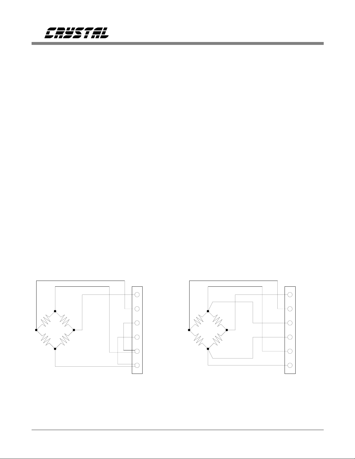
CDB5516/CDB5520
ample, the board comes with a set of precision
resistors which divide the excitation supply
(nominally 10 volts total) down to 2.5 volts between the VREF+ and VREF- input pins. This
sets the nominal full scale voltage into the A/D
converter. The input span of the instrumentation
amplifier can be calculated to by knowing the
PGA gain setting, and that the gain of the instrumentation amplifier is X25. If the PGA is set for
a gain of 8, then the input span to the instrumentation amplifier will be 2.5 volts (VREF+ VREF-) divided by 8 X 25, or 2.5/(200) = 12.5
millivolt nominal in unipolar mode. The device
can be then calibrated with an input voltage
which is as low as 20% less than nominal or up
to 20% greater than nominal. Therefore, with
this VREF+ - VREF- voltage (2.5 volts) and a
PGA gain of 8 the input span can be calibrated
to handle a span from a low of 10 mV to a high
of 15 mV. To modify the input span the user can
either change the PGA gain or modify the resistor divider on the bridge sense voltage to yield
an appropriate value in the range of 2.0 to 3.8
volts. This makes the A/D converter quite flex-
ible in handling load cells with different output
levels. Whenever configured as a bridge
transducer device, the CS5516 or the CS5520
A/D converter operates in ratiometric measurement mode. Figures 4 and 5 illustrate how to
connect 4-wire and 6-wire bridge transducers to
the board.
Alternatively, the CS5516 or CS5520 can be
configured for absolute measurement if a precision reference voltage is supplied between the
VREF+ and VREF- pins of the A/D converter.
The board can be modified to accept a reference
into the voltage reference terminal block; or the
on-board LT1019-2.5 volt reference can be used
as the reference voltage for the A/D converter.
To use either of these inputs will require that
jumper wires be soldered in either 1A-1B to select the external voltage reference input, or
2A-2B to select the on-board LT1019-2.5. Figure 6 illustrates the connection of an external
voltage reference to the evaluation board for absolute voltage measurement applications. To
achieve an accurate reference voltage resistor R6
SIG +
SIG -
SENSE +
_
Figure 4. 4-Wire Bridge Connections
DS74DB3 35
+
SENSE -
EXC +
EXC -
_
Figure 5. 6-Wire Bridge Connections
+
SIG +
SIG -
SENSE +
SENSE -
EXC +
EXC -
Page 36
CDB5516/CDB5520
must be removed from between the +VREF and
-VREF pins. It may be desirable to also remove
R5, R7, C16, and C17 in some applications.
Calibrating the A/D Converter
As explained in the CS5516/CS5520 data sheet,
the order in which the calibration steps are performed are important. If one chooses to use the
non-ratiometric calibration capabilities of the
converter, the non-ratiometric errors of the
VREF and AIN channels should be calibrated
first. The non-ratiometric calibration steps can
be performed at the same time. Before the nonratiometric offset calibration is initiated, the
bridge should be grounded. This can be achieved
on the evaluation board by moving the two
jumpers at the output of the MIC4428 driver to
the GND position (see Figure 1). The converter
is then instructed via the configuration register
bits to perform the non-ratiometric calibration
steps. Once the non-ratiometric calibrations are
completed, jumpers at the output of the
MIC4428 driver should be returned to the EXC
position.
After the non-ratiometric calibration steps are
performed, the AIN ratiometric offset is then
calibrated. With "zero weight" on the load cell,
the converter is instructed via the configuration
register to perform the AIN ratiometric offset
calibration step. Finally, with "full scale weight"
on the load cell, the converter is instructed to
perform the gain calibration step.
The converter is then ready to perform conversions.
Software
The evaluation board comes with software and a
RS-232 cable to interface the board to a RS-232
port of a PC-compatible computer. The software
diskette contains a README.TXT file which
explains its operation.
+5V
Z1
AGND
+5VA
+
C3
47µF
C4
0.1µF
+5
Z3
+
C5
47µF
0.1µF
DGND
+5VD
C6
+
Z2
C1
47µF
C2
0.1µF
-5VA-5V
Figure 6. Using Off -board Volta ge Refere nce
36 DS74DB3
Page 37
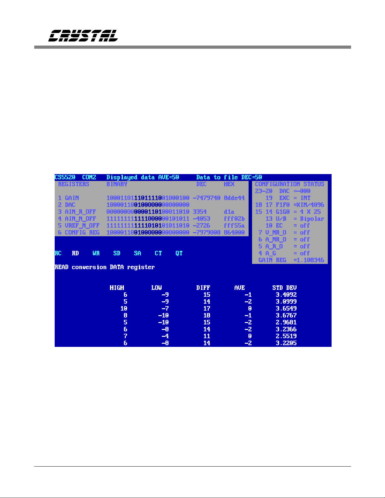
Figure 7 illustrates the software supplied with
the CDB5516/CDB5520 evaluation board. The
software allows the user to manipulate the registers of the converter and perform calibrations
and conversions. It decodes the status of the configuration register and indicates the gain register
scale factor. The software enables the user to
collect data to a file, average samples and compute the average and standard deviation of the
samples which have been collected.
CDB5516/CDB5520
Figure 7. Screen for the CDB5516 /CDB5520 Ev aluation Board Softwa re
DS74DB3 37
Page 38

CDB5516/CDB5520
Figure 8. CDB 55 20 Sil ks creen
38 DS74DB3
Page 39

CDB5516/CDB5520
Figure 9. CDB55 20 Top Gr ound Pl ane
DS74DB3 39
Page 40

CDB5516/CDB5520
Figure 10. CDB5520 Solder Side Trace Layer
40 DS74DB3
Page 41

• Notes •
Page 42

 Loading...