

Datasheet CS52015-1GT3, CS52015-1GSTR3, CS52015-1GST3, CS52015-1GDPR3, CS52015-1GDP3 Datasheet (Cherry Semiconductor)
Page 1
Cherry Semiconductor Corporation
2000 South County Trail, East Greenwich, RI 02818
Tel: (401)885-3600 Fax: (401)885-5786
Email: info@cherry-semi.com
Web Site: www.cherry-semi.com
1
Features
■ Output Current to 1.5A
■ Output Accuracy to ±1%
Over Temperature
■ Dropout Voltage (typical)
1.05V @ 1.5A
■ Fast Transient Response
■ Fault Protection
Current Limit
Thermal Shutdown
Package Options
3L TO-220
Tab (V
OUT
)
CS52015-1
1.5A Adjustable Linear Regulator
1
CS52015-1
The CS52015-1 linear regulator provides 1.5A with an accuracy of ±1%.
The device uses two external resistors to set the output voltage within
a 1.25V to 5.5V range.
The regulator is intended for use as
a post regulator and microprocessor
supply. The fast loop response and
low dropout voltage make this regulator ideal for applications where
low voltage operation and good
transient response are important.
The circuit is designed to operate
with dropout voltages less than
1.4V at 1.5A output current. Device
protection includes overcurrent and
thermal shutdown.
The CS52015-1 is pin compatible
with the LT1086 family of linear
regulators but has lower dropout
voltage.
The regulator is available in TO220, surface mount D2, and SOT-223
packages.
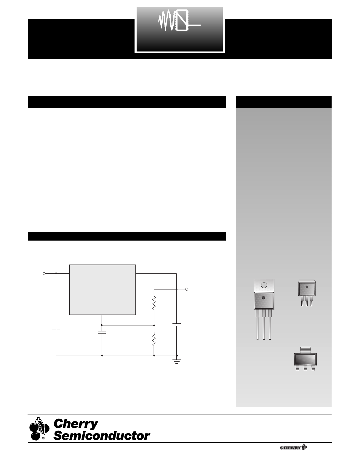
Application Diagram
Consult factory for fixed output voltage
versions.
CS52015 -1
1 Adj
2V
OUT (Tab)
3V
IN
Description
3L D2PAK
Tab (V
OUT
)
1
A Company
¨
SOT-223
Tab (V
OUT
)
1
Rev. 2/17/98
5.0V
V
IN
CS52015-1
V
OUT
3.3V @ 1.5A
10 mF
5V
Adj
0.1mF
5V
Tantalum
124W
1%
200W
1%
22mF
5V
Page 2
2
CS52015-1
Absolute Maximum Ratings
Supply Voltage, V
CC
....................................................................................................................................................................7V
Operating Temperature Range................................................................................................................................-40¡C to 70¡C
Junction Temperature ............................................................................................................................................................150¡C
Storage Temperature Range ..................................................................................................................................-60¡C to 150¡C
Lead Temperature Soldering
Wave Solder (through hole styles only) .....................................................................................10 sec. max, 260¡C peak
Reflow (SMD styles only) ......................................................................................60 sec. max above 183¡C, 230¡C peak
ESD Damage Threshold............................................................................................................................................................2kV
PACKAGE PIN # PIN SYMBOL FUNCTION
PARAMETER TEST CONDITIONS MIN TYP MAX UNIT
Electrical Characteristics: C
IN
= 10µF, C
OUT
= 22µF Tantalum, V
OUT
+ V
DROPOUT
< VIN< 7V, 0¡C ² TA ² 70¡C, TJ² +150¡C,
unless otherwise specified, I
full load
= 1.5A.
Package Pin Description
■ Adjustable Output Voltage (CS52015-1)
Reference Voltage V
INÐVOUT
=1.5V; V
Adj
= 0V 1.241 1.254 1.266 V
(Notes 1 and 2) 10mA²I
OUT
²1.5A (-1%) (+1%)
Line Regulation 1.5V²VINÐV
OUT
²5.75V; I
OUT
=10mA 0.02 0.20 %
Load Regulation VINÐV
OUT
=1.5V; 10mA²I
OUT
²1.5A 0.04 0.4 %
(Notes 1 and 2)
Dropout Voltage (Note 3) I
OUT
=1.5A 1.05 1.4 V
Current Limit VINÐV
OUT
=3V; TJ³ 25¡C 1.6 3.1 A
Minimum Load Current (Note 4) VIN=7V ; V
Adj
=0 0.6 2.0 mA
Adjust Pin Current VINÐV
OUT
=3V; I
OUT
=10mA 50 100 µA
Thermal Regulation (Note 5) 30ms pulse; TA=25¡C 0.002 0.020 %/W
Ripple Rejection (Note 5) f=120Hz; I
OUT
=1.5A; VINÐV
OUT
=3V; 80 dB
V
RIPPLE
=1V
PP
Thermal Shutdown (Note 6) 150 180 210 ¡C
Thermal Shutdown Hysteresis 25 ¡C
(Note 6)
Note 1: Load regulation and output voltage are measured at a constant junction temperature by low duty cycle pulse testing. Changes in out-
put voltage due to temperature changes must be taken into account separately.
Note 2: Specifications apply for an external Kelvin sense connection at a point on the output pin 1/4Ó from the bottom of the package.
Note 3: Dropout voltage is a measurement of the minimum input/output differential at full load.
Note 4: The minimum load current is the minimum current required to maintain regulation. Normally the current in the resistor divider used
to set the output voltage is selected to meet the minimum requirement.
Note 5: Guaranteed by design, not 100% tested in production.
Note 6: Thermal shutdown is 100% functionally tested in production.
D2PAK TO-220 SOT-223
1 1 1 Adj Adjust pin (low side of the internal reference.
222V
OUT
Regulated output voltage (case).
333VINInput voltage
Page 3
CS52015-1
3
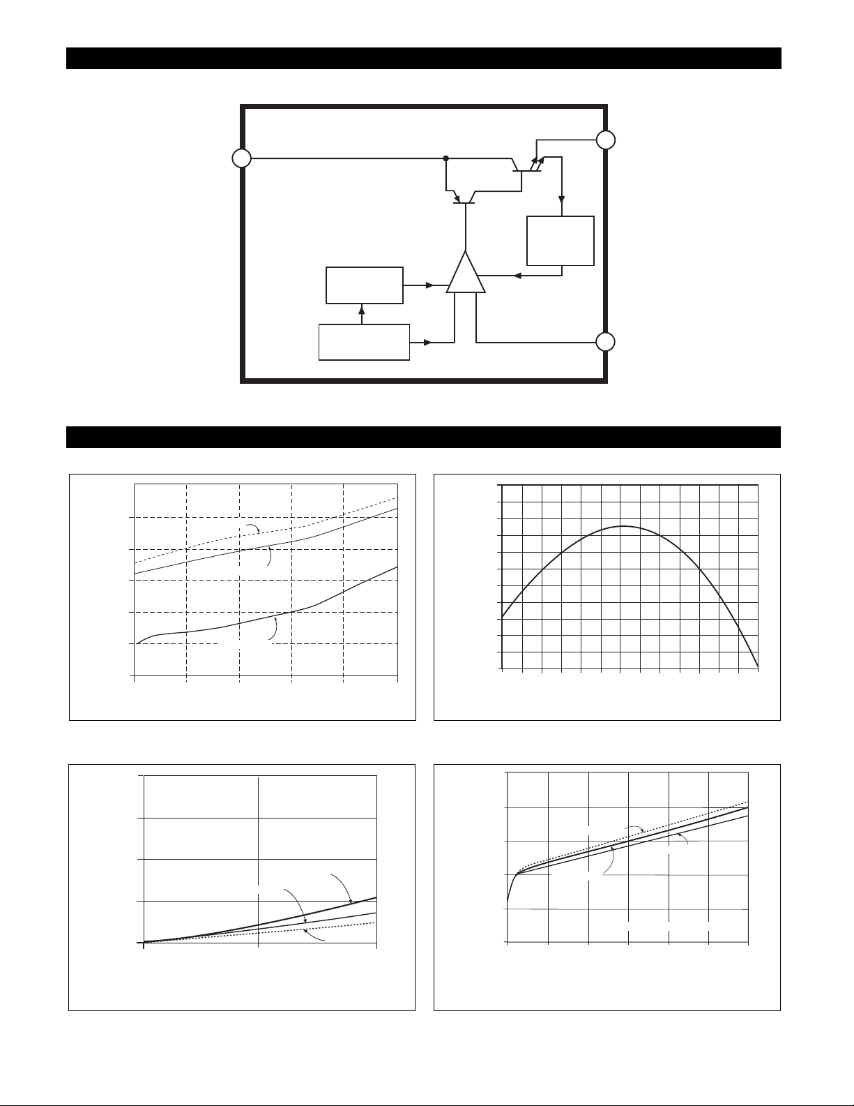
Block Diagram
Dropout Voltage vs. Output Current Reference Voltage vs. Temperature
Load Regulation vs. Output Current
Minimum Load Current vs VIN-V
OUT
Typical Performance Characteristics
V
OUT
V
IN
Output
Current
Limit
Thermal
Shutdown
-
+
Error
Amplifier
1.05
1.00
0.95
0.90
V Drop Out (V)
0.85
0.80
0.75
T
CASE
T
T
0ûC
CASE
CASE
25ûC
125ûC
I
OUT
Bandgap
150012009006003000
(mA)
Adj
0.10
0.08
0.06
0.04
0.02
0.00
-0.02
-0.04
-0.06
Output Voltage Deviation (%)
-0.08
-0.10
-0.12
0 10 130
20 30 40 50 60 70 80 90 100 110 120
TJ (°C)
0.100
0.075
0.050
T
= 25°C
0.025
Output Voltage Deviation (%)
0.000
012
CASE
Output Current (A)
T
CASE
= 125°C
T
CASE
= 0°C
0.65
0.60
T
CASE
T
= 25°C
0.55
0.50
Minimum Load Current (mA)
0.45
0.40
123456
CASE
= 0°C
VIN – V
OUT
T
C
IN =COUT
(V)
= 125°C
CASE
=22mF Tantalum
7
Page 4

4
CS52015-1
Applications Information
The CS52015-1 linear regulator provides adjustable voltages at currents up to 1.5A. The regulator is protected
against overcurrent conditions and includes thermal
shutdown.
The CS52015-1 has a composite PNP-NPN output transistor
and requires an output capacitor for stability. A detailed
procedure for selecting this capacitor is included in the
Stability Considerations section.
The 52015-1 has an output voltage range of 1.25V to 5.5V.
An external resistor divider sets the output voltage as
shown in Figure 1. The regulator maintains a fixed 1.25V
(typical) reference between the output pin and the adjust
pin.
A resistor divider network R1 and R2 causes a fixed current to flow to ground. This current creates a voltage
across R2 that adds to the 1.25V across R1 and sets the
overall output voltage. The adjust pin current (typically
50µA) also flows through R2 and adds a small error that
should be taken into account if precise adjustment of V
OUT
is necessary.
The output voltage is set according to the formula:
V
OUT
= V
REF
´
()
+ I
Adj
´ R2
The term I
Adj
´ R2 represents the error added by the adjust
pin current.
R1 is chosen so that the minimum load current is at least
2mA. R1 and R2 should be the same type, e.g. metal film
for best tracking over temperature. While not required, a
bypass capacitor from the adjust pin to ground will
improve ripple rejection and transient response. A 0.1µF
tantalum capacitor is recommended for Òfirst cutÓ design.
Type and value may be varied to obtain optimum performance vs price.
R1 + R2
R1
Adjustable Operation
Adjust Pin Current vs. Temperature Ripple Rejection vs. Frequency
Transient Response
Short Circuit Current vs VIN-V
OUT
Typical Performance Characteristics
Adjust Pin Current (mA)
70.0
65.0
60.0
55.0
50.0
45.0
IO = 10mA
85
75
65
55
45
Ripple Rejection (dB)
35
25
T
CASE
I
OUT
(V
IN
V
RIPPLE
C
Adj
= 25°C
= 1.5A
Ð V
OUT
= 1.0V
= 0.1mF
) = 3V
PP
40.0
02030405060
10 70
Temperature (°C)
90
100
80
110
120
130
200
100
0
Voltage Deviation (mV)
-100
-200
1500
750
0
Load Step (mA)
023456
V
C
C
Time mS
=3.3V
OUT
OUT =CIN
=0.1mF
Adj
=22mF Tantalum
7
10981
15
1
10
3.5
3.3
3.1
2.9
2.7
2.5
(A)
SC
I
2.3
2.1
1.9
1.7
1.5
1.0 4.0
2
10
1.5 2.5 3.0 3.5
2.0 4.5 5.0 6.05.5 6.5 7.0
3
10
Frequency (Hz)
VIN - V
OUT
4
10
(V)
5
10
6
10
Page 5

5
CS52015-1
Applications Information: continued
Figure 1. Resistor divider scheme.
The CS52015-1 linear regulator has an absolute maximum
specification of 7V for the voltage difference between V
IN
and V
OUT
. However, the IC may be used to regulate voltages in excess of 7V. The main considerations in such a
design are power-up and short circuit capability.
In most applications, ramp-up of the power supply to V
IN
is fairly slow, typically on the order of several tens of milliseconds, while the regulator responds in less than one
microsecond. In this case, the linear regulator begins
charging the load as soon as the VINto V
OUT
differential is
large enough that the pass transistor conducts current. The
load at this point is essentially at ground, and the supply
voltage is on the order of several hundred millivolts, with
the result that the pass transistor is in dropout. As the supply to VINincreases, the pass transistor will remain in
dropout, and current is passed to the load until V
OUT
reaches the point at which the IC is in regulation. Further
increase in the supply voltage brings the pass transistor
out of dropout. The result is that the output voltage follows the power supply ramp-up, staying in dropout until
the regulation point is reached. In this manner, any output
voltage may be regulated. There is no theoretical limit to
the regulated voltage as long as the VINto V
OUT
differen-
tial of 7V is not exceeded.
However, the possibility of destroying the IC in a short
circuit condition is very real for this type of design. Short
circuit conditions will result in the immediate operation of
the pass transistor outside of its safe operating area. Overvoltage stresses will then cause destruction of the pass
transistor before overcurrent or thermal shutdown circuitry can become active. Additional circuitry may be required
to clamp the VINto V
OUT
differential to less than 7V if failsafe operation is required. One possible clamp circuit is
illustrated in figure 2; however, the design of clamp circuitry must be done on an application by application basis.
Care must be taken to ensure the clamp actually protects
the design. Components used in the clamp design must be
able to withstand the short circuit condition indefinitely
while protecting the IC.
Figure 2: Short Circuit Protection Circuit for High Voltage Application.
The output or compensation capacitor helps determine
three main characteristics of a linear regulator: start-up
delay, load transient response and loop stability.
The capacitor value and type is based on cost, availability,
size and temperature constraints. A tantalum or aluminum
electrolytic capacitor is best, since a film or ceramic capacitor with almost zero ESR can cause instability. The aluminum electrolytic capacitor is the least expensive solution. However, when the circuit operates at low temperatures, both the value and ESR of the capacitor will vary
considerably. The capacitor manufacturersÕ data sheet provides this information.
A 22µF tantalum capacitor will work for most applications,
but with high current regulators such as the CS52015-1 the
transient response and stability improve with higher values of capacitance. The majority of applications for this
regulator involve large changes in load current so the output capacitor must supply the instantaneous load current.
The ESR of the output capacitor causes an immediate drop
in output voltage given by:
ÆV = ÆI ´ ESR
For microprocessor applications it is customary to use an
output capacitor network consisting of several tantalum
and ceramic capacitors in parallel. This reduces the overall
ESR and reduces the instantaneous output voltage drop
under load transient conditions. The output capacitor network should be as close as possible to the load for the best
results.
When large external capacitors are used with a linear regulator it is sometimes necessary to add protection diodes. If
the input voltage of the regulator gets shorted, the output
capacitor will discharge into the output of the regulator.
The discharge current depends on the value of the capacitor, the output voltage and the rate at which V
IN
drops. In
the CS52015-1 linear regulator, the discharge path is
through a large junction and protection diodes are not usually needed. If the regulator is used with large values of
output capacitance and the input voltage is instantaneously shorted to ground, damage can occur. In this case, a
diode connected as shown in Figure 2 is recommended.
Protection Diodes
Stability Considerations
V
IN
C
1
V
IN
CS52015-1
Adj
V
OUT
V
REF
R
1
I
Adj
R
C
Adj
2
V
OUT
C
2
EXTERNAL SUPPLY
V
IN
V
OUT
V
Adj
V
OUT
Page 6

6
CS52015-1
Figure 3. Protection diode scheme for Large Output Capacitors.
Since the CS52015-1 is a three terminal regulator, it is not
possible to provide true remote load sensing. Load regulation is limited by the resistance of the conductors connecting the regulator to the load.
For the adjustable regulator, the best load regulation occurs
when R1 is connected directly to the output pin of the regulator as shown in Figure 3. If R1 is connected to the load,
RCis multiplied by the divider ratio and the effective resistance between the regulator and the load becomes
R
C
´
()
RC= conductor parasitic resistance
Figure 4. Grounding scheme for the adjustable output regulator to minimize parasitic resistance effects.
The CS52015-1 linear regulator includes thermal shutdown
and current limit circuitry to protect the device. High
power regulators such as these usually operate at high
junction temperatures so it is important to calculate the
power dissipation and junction temperatures accurately to
ensure that an adequate heat sink is used.
The case is connected to V
OUT
on the CS52015-1, and elec-
trical isolation may be required for some applications.
Thermal compound should always be used with high current regulators such as these.
The thermal characteristics of an IC depend on the following four factors:
1. Maximum Ambient Temperature T
A
(¡C)
2. Power dissipation P
D
(Watts)
3. Maximum junction temperature T
J
(¡C)
4. Thermal resistance junction to ambient R
QJA
(C/W)
These four are related by the equation
TJ= TA+ PD´ R
QJA
(1)
The maximum ambient temperature and the power dissipation are determined by the design while the maximum
junction temperature and the thermal resistance depend on
the manufacturer and the package type.
The maximum power dissipation for a regulator is:
P
D(max)
={V
IN(max)ÐVOUT(min)}IOUT(max)+VIN(max)IQ
(2)
where
V
IN(max)
is the maximum input voltage,
V
OUT(min)
is the minimum output voltage,
I
OUT(max)
is the maximum output current, for the application
I
Q
is the maximum quiescent current at I
OUT
(max).
A heat sink effectively increases the surface area of the
package to improve the flow of heat away from the IC and
into the surrounding air.
Each material in the heat flow path between the IC and the
outside environment has a thermal resistance. Like series
electrical resistances, these resistances are summed to
determine R
QJA
, the total thermal resistance between the
junction and the surrounding air.
1. Thermal Resistance of the junction to case, R
QJC
(¡C/W)
2. Thermal Resistance of the case to Heat Sink, R
QCS
(¡C/W)
3. Thermal Resistance of the Heat Sink to the ambient air,
R
QSA
(¡C/W)
These are connected by the equation:
R
QJA
= R
QJC
+ R
QCS
+ R
QSA
(3)
The value for R
QJA
is calculated using equation (3) and the
result can be substituted in equation (1).
The value for R
QJC
is 3.5ûC/W. For a high current regulator such as the CS52015-1 the majority of the heat is generated in the power transistor section. The value for R
QSA
depends on the heat sink type, while R
QCS
depends on factors such as package type, heat sink interface (is an insulator and thermal grease used?), and the contact area
between the heat sink and the package. Once these calculations are complete, the maximum permissible value of R
QJA
can be calculated and the proper heat sink selected. For further discussion on heat sink selection, see application note
ÒThermal Management for Linear Regulators.Ó
Calculating Power Dissipation and Heat Sink Requirements
R1 + R2
R1
Output Voltage Sensing
V
Applications Information: continued
IN
IN4002 (optional)
V
IN
C
1
CS52015-1
Adj
V
OUT
R
1
R
C
Adj
2
V
C
2
OUT
V
IN
Adj
V
OUT
V
IN
CS52015-1
R
C
R
1
conductor parasitic
resistance
R
LOAD
R
2
Page 7

3L 3L 3L
Thermal Data TO-220 D2PAK SOT-223
R
QJC
typ 3.5 3.5 15 ûC/W
R
QJA
typ 50 10 - 50* 156 ûC/W
*Depending on thermal properties of substrate. R
QJA
= R
QJC
+ R
QCA
7
Part Number Type Description
CS52015-1GT3 1.5A, adj. output 3 L TO-220 Straight
CS52015-1GDP3 1.5A, adj. output 3 L D2PAK
CS52015-1GDPR3 1.5A, adj. output 3 L D
2
PAK
(tape & reel)
CS52015-1GST3 1.5A, adj. output SOT-223
CS52015-1GSTR3 1.5A, adj. output SOT-223 (tape & reel)
Ordering Information
Rev. 2/17/98
Package Specification
PACKAGE THERMAL DATA
CS52015-1
© 1999 Cherry Semiconductor Corporation
Cherry Semiconductor Corporation reserves the
right to make changes to the specifications without
notice. Please contact Cherry Semiconductor
Corporation for the latest available information.
PACKAGE DIMENSIONS IN mm (INCHES)
3 Lead D2PAK (DP)
2.54 (.100) REF
10.31 (.406)
10.05 (.396)
8.53 (.336)
8.28 (.326)
0.91 (.036)
0.66 (.026)
1.40 (.055)
1.14 (.045)
4.57 (.180)
4.31 (.170)
1.68 (.066)
1.40 (.055)
2.74(.108)
2.49(.098)
1.40 (.055)
1.14 (.045)
0.10 (.004)
0.00 (.000)
.254 (.010) REF
15.75 (.620)
14.73 (.580)
2.79 (.110)
2.29 (.090)
3 Lead TO-220 (T) Straight
5.33 (.210)
4.83 (.190)
2.79 (.110)
2.29 (.090)
1.02 (.040)
0.63 (.025)
0.56 (.022)
0.38 (.014)
1.40 (.055)
1.14 (.045)
4.83 (.190)
4.06 (.160)
6.17 (.243) REF
1.14 (.045)
1.52 (.060)
1.14 (.045)
1.40 (.055)
2.87 (.113)
2.62 (.103)
6.55 (.258)
5.94 (.234)
14.22 (.560)
13.72 (.540)
2.92 (.115)
2.29 (.090)
9.78 (.385)
10.54 (.415)
3.71 (.146)
3.96 (.156)
14.99 (.590)
14.22 (.560)
3 Lead SOT-223 (ST)
10° MAX
1.30 (.051)
1.10 (.043)
4.60 (.181)
2.30 (.090)
1.05 (.041)
0.85 (.033)
7.30 (.287)
6.70 (.264)
3.30 (.130)
3.70 (.146)
3.15 (.124)
2.95 (.116)
6.70 (.264)
6.30 (.248)
1.70 (.067)
1.50 (.060)
0.10 (.004)
0.02 (.001)
0.85 (.033)
0.65 (.026)
0.35 (.014)
0.25 (.010)
 Loading...