

Page 1
CS5180
∆Σ Modulator & 8 kHz to 400 kHz 16-Bit ADC
Features
16-Bit Delta-Sigma A/D Converter
Fully Differential Input with 4.0 VppRange
Dynamic Range: 93 dB
Spurious Free Dynamic Range: 96 dB
Total Harmonic Distortion: -95 dB @ 22 kHz
Up to 400 kHz Output Word Rate
No Missing Codes
Non-Aliasing Low-Pass Digital Filter
High Speed 3-Wire Serial Interface
Supply Options:
- VA+=5V,VD+=5V,690mW
- VA+=5V,VD+=3V,368mW
Modulator Output Mode
Power Down Mode
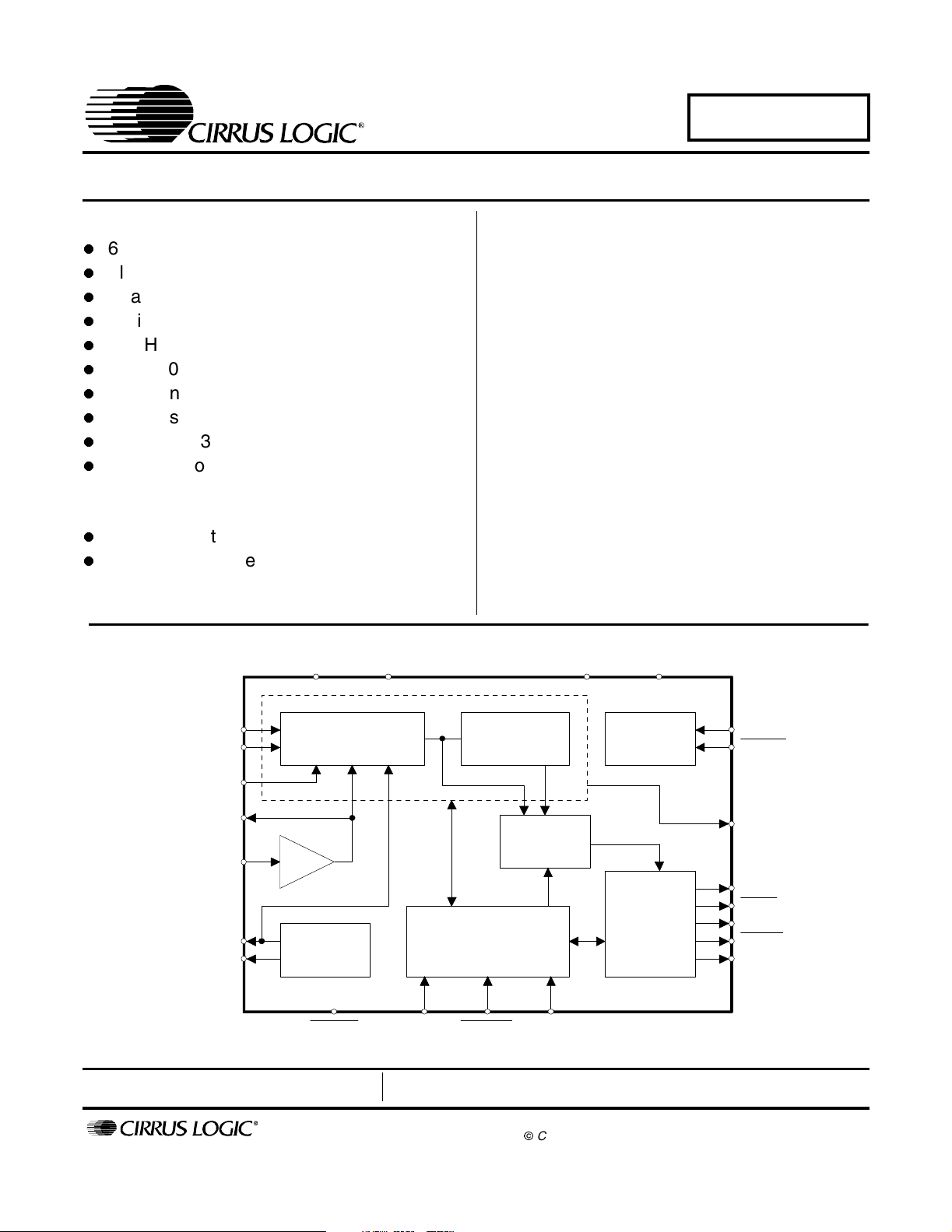
I
VA+
AGND
Description
CS5180 is a fully calibrated high-speed ∆Σ analog-todigital converter, capable of 400 kSamples/second output word rate (OWR). The OWR scales with the master
clock. It consists of a 5th order ∆Σ modulator, decimation
filter, and serial interface. The chip can use the 2.375 V
on-chip voltage reference, or an external 2.5 V reference. The input voltage range is 1.6 × VREFIN V
differential. Multiple CS5180s can be fully synchronized
in multi-channel applications with a SYNC signal. The
part has a power-down mode to minimize power consumption at times of system inactivity. The high speed
digital I/O lines have complementary signals to help reduce radiated noise from traces on the PC board. The
CS5180 can also be operated in modulator-only mode
which provides the delta-sigma modulator bitstream as
the output.
ORDERING INFORMATION
CS5180-CL 0 °C to 70 °C 28-pin PLCC
VD+
DGND
pp
fully
AIN+
AIN-
VREF-
VREF+
VREFIN
VREFOUT
VREFCAP
x1.6
Reference
∆Σ
Modulator
PWDN SYNC RESET MODE
Preliminary Product Information
P.O. Box 17847, Austin, Texas 78760
(512) 445 7222 FAX: (512) 445 7581
http://www.cirrus.com
Decimator Clock
Mode
Selector
Timing
and
Control
Cirrus Logic reserves the right to modify this product without notice.
CopyrightCirrus Logic, Inc. 2002
(All Rights Reserved)
Serial
Interface
MCLK
MCLK
MFLAG
SDO
SDO
SCLK
SCLK
FSO
DS259PP4
APR ‘02
1
Page 2

TABLE OF CONTENTS
CHARACTERISTICS/SPECIFICATIONS ............................................................4
ANALOG CHARACTERISTICS...................................................................4
DYNAMIC CHARACTERISTICS ................................................................. 6
DIGITAL CHARACTERISTICS.................................................................... 6
SWITCHING CHARACTERISTICS ............................................................. 7
RECOMMENDED OPERATING CONDITIONS .......................................... 8
ABSOLUTE MAXIMUM RATINGS.............................................................. 8
GENERAL DESCRIPTION .................................................................................. 9
THEORY OF OPERATION .................................................................................. 9
Converter Initialization: Calibration and Synchronization .......................... 9
Clock Generator ........................................................................................ 10
Voltage Reference .................................................................................... 10
Analog Input ............................................................................................. 11
Output Coding .......................................................................................... 11
Modulator-Only mode ............................................................................... 11
Instability Indicator .................................................................................... 13
Digital Filter Characteristics ...................................................................... 13
Serial Interface .......................................................................................... 13
Power Supplies / Board Layout ................................................................ 13
Power-down Mode .................................................................................... 15
PIN DESCRIPTION ............................................................................................ 16
PARAMETER DEFINITIONS ............................................................................. 19
APPENDIX A: CIRCUIT APPLICATIONS ......................................................... 21
PACKAGE OUTLINE DIMENSIONS ................................................................. 26
CS5180
Contacting Cirrus Logic Support
For a complete listing of Direct Sales, Distributor, and Sales Representative contacts, visit the Cirrus Logic web site at:
http://www.cirrus.com/corporate/contacts/sales.cfm
IMPORTANT NOTICE
"Preliminary" product inf ormation describes products that are in production, but for which full characterization data is not yet available. "Advance" product inf ormation describes products that are in development and subject to devel opment changes. Cirrus Logi c, I nc. and its subsi diari es ("Cirrus") believe that the inf ormation contained in this document is accurate and reliable. However, the information is subject to change without notice and is provided "AS IS" without warranty
of any kind (express or implied). Customers are advised to obtain the latest version of relevant information to verify, befor e placing orders, that information being
relied on is current and complete. All products are sold subj ect to the terms and conditions of sal e supplied at the time of order acknowledgment, including those
pertaining to warranty, patent infringement, and limitation of liability. No responsibility is assumed by Cirrus for the use of this information, i ncludi ng use of this
information as the basis for manufacture or sale of any items, or for i nfringement of patents or other rights of third parties. This document is the property of Cirrus
and by furnishi ng th is information, Cirrus grants no license, express or implied under any patents, mask work rights, copyrights, trademarks, tr ade secrets or
other intellectual property rights. Cirrus owns the copyrights of the information contained herein and gi ves consent for copies to be made of the i nformation only
for use within your organization with respect to Ci rrus integrat ed circuits or ot her parts of Cirrus. This consent does not extend to other copying such as copying
for general distribution, advertising or promotional p urposes, or for creating any work for resale.
An export permit needs to be obtained from the competent authorities of the Japanese Government if any of the products or technologies described in thismaterial and controll ed under the "Foreign Exchange and Forei gn Trade Law" i s to be exported or taken out of Japan. An export l icense and/or quota needs to be
obtained from the competent authorities of the Chinese Government if any of the products or technologies describe d in this material is subject to the PRC Foreign
Trade Law and i s to be exported or taken out of the PRC.
CERTAIN APPLICATIONS USING SEMICONDUCTOR PRODUCTS MAY INVOLVE POTENTIAL RISKS OF DEATH, PERSONAL INJURY, OR SEVERE
PROPERTY OR ENVIRONMENTAL DAMAGE ("CRITICAL APPLICATIONS"). CIRRUS PRODUCTS ARE NOT DESIGNED, AUTHORIZED, OR WARRANTED TO BE SUITABLE FOR USE IN LIFE-SUPPORT DEVICES OR SYSTEMS OR OTHER CRITICAL APPLICATIONS. INCLUSION OF CIRRUS PRODUCTS
IN SUCH APPLICATIONS IS UNDERSTOOD TO BE FULLY AT THE CUSTOMER'S RISK.
Cirrus Logic, Cirrus, and the Cirrus Logi c logo designs are trademarks of Cirrus Logic, Inc. All other brand and product names in this document may be trademarks or service marks of their respective owners.
2
Page 3

LIST OF FIGURES
Figure 1. Serial Port Timing (not to scale) .................................................................. 7
Figure 2. RESET and SYNC logic and timing. ........................................................... 9
Figure 3. CS5180 connection diagram for using the internal voltage reference. ...... 10
Figure 4. CS5180 connection diagram for using an external voltage reference. ...... 11
Figure 5. Modulator Only Mode Data RTZ Format. .................................................. 12
Figure 6. Circuit to Reconstruct
Return-to-Zero (RTZ) Data from SDO/SDO into Original Modulator Bitstream. 12
Figure 7. Magnitude versus frequency spectrum of modulator
bitstream (MCLK = 25.6 MHz). .......................................................................... 12
Figure 8. Expanded view of the magnitude versus frequency spectrum of
modulator bitstream (MCLK = 25.6 MHz). ......................................................... 12
Figure 9. CS5180 Digital Filter Magnitude Response (MCLK = 25.6 MHz) .............. 13
Figure 10. CS5180 Digital Filter Phase Response
(MCLK = 25.6 MHz) ........................................................................................... 13
Figure 11. CS5180 System Connection Diagram ..................................................... 14
Figure 12. Single amplifier driving only AIN+, AIN- held at steady dc value ............. 21
Figure 13. Performance of amplifier of Figure 12 overdriving AIN+ input to the
CS5180 at 4 VPP ............................................................................................... 21
Figure 14. Performance of amplifier of Figure 12 with AIN+ driven at 2 VPP ........... 21
Figure 15. AC-coupled driver using two amplifiers. .................................................. 22
Figure 16. Performance of amplifier in Figure 15 ..................................................... 22
Figure 17. Three amplifier driver .............................................................................. 23
Figure 18. Performance of amplifier in Figure 17 ..................................................... 23
Figure 19. Four amplifier driver. ............................................................................... 24
Figure 20. Performance of amplifier in Figure 19 ..................................................... 24
Figure 21. Performance of amplifier in Figure 19 ..................................................... 24
Figure 22. CS5180 Differential Non-linearity plot.
(Data taken with repeating ramp) ....................................................................... 25
Figure 23. Histogram of DNL from Figure 22 ........................................................... 25
Figure 24. CS5180 Noise Histogram, > 60,000 samples. ........................................ 25
CS5180
3
Page 4
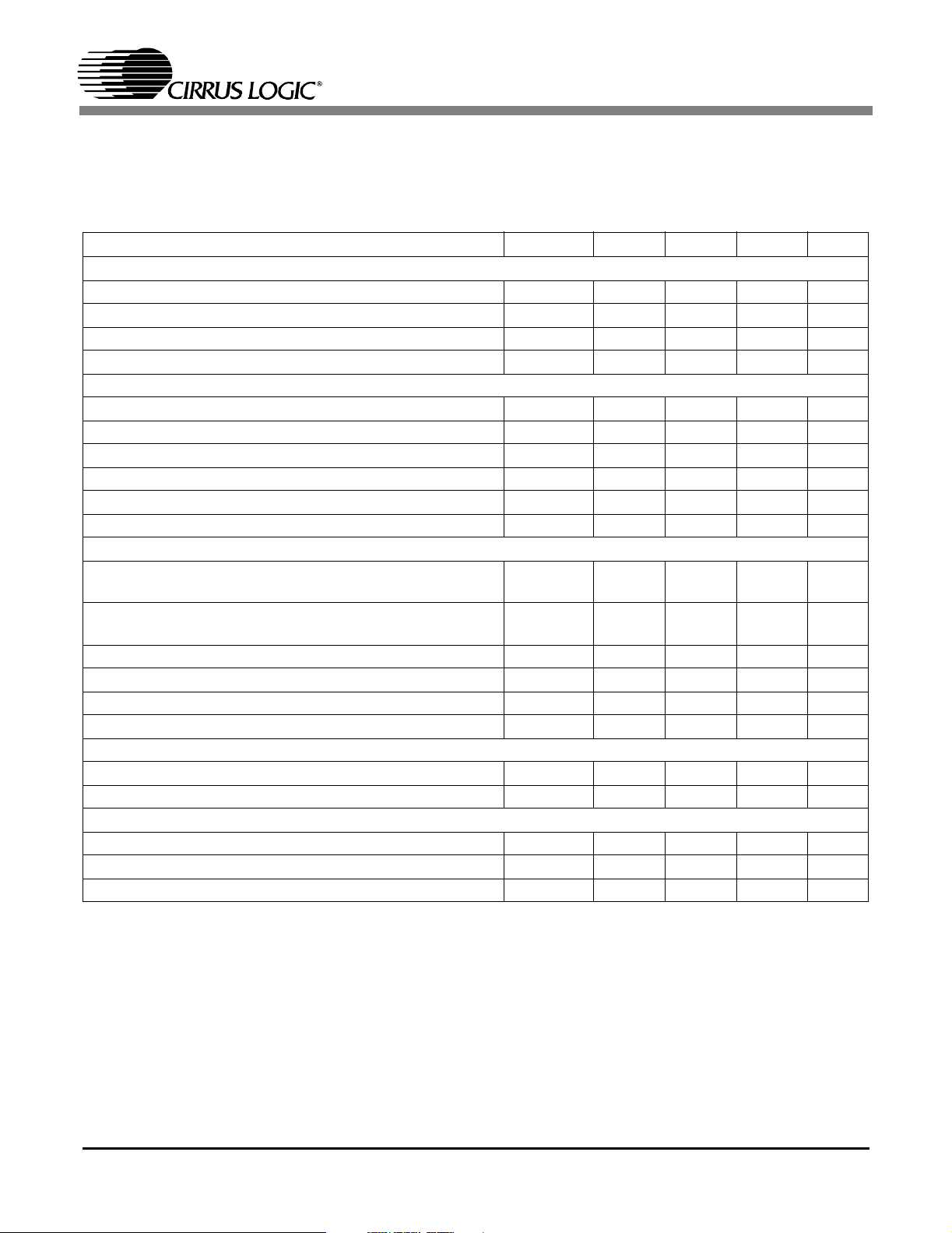
CHARACTERISTICS/SPECIFICATIONS
CS5180
ANALOG CHARACTERISTICS (T
DGND = 0 V; MCLK = 25.6 MHz; VREFIN = VREFOUT; MODE = VD+; Analog source impedance = 301 Ohms
with 2200 pF to AGND; Full-Scale input sinewave at 22 kHz; Unless otherwise noted)
Parameter Symbol Min Typ Max Unit
Dynamic Performance
Dynamic Range (Note 1) DR 90 93 - dB
Total Harmonic Distortion THD -90 -95 - dB
Signal to (Noise + Distortion) SINAD 87 91 - dB
Spurious Free Dynamic Range SFDR 90 96 - dBc
Static Performance
Linearity Error (Note 2) INL - ±2 - LSB
Differential Non-Linearity (Note 2) DNL - - ±0.5 LSB
Full Scale Error (Note 6) - ±8 - LSB
Full Scale Drift with Internal Reference (Notes 2 and 5) - ±50 - ppm/°C
Offset Error (Note 6) - ±8 - LSB
Offset Drift (Note 2) - ±6.0 - µV/°C
Analog Input
Differential Input Voltage Range (Note 3) - 1.6 X
Common Mode Range CMR 1 - VREFIN
Input Capacitance - 4.0 - pF
Differential Input Impedance MCLK = 25.6 MHz - 500 - kΩ
Common Mode Rejection Ratio (Note 2) CMRR 50 - - dB
Common Mode Input Current MCLK = 25.6 MHz - ±100 ±200 µA
Reference Input
VREFIN 2.25 2.375 2.6 V
VREFIN Current (Note 4) - 1 ±200 µA
Reference Output
VREFOUT Voltage 2.25 2.375 2.5 V
VREFOUT Output Current - - ±500 µA
VREFOUT Impedance - 0.1 - Ω
= 0 °C to 70 °C; VA+ = 5 V ± 5%, VD+ = 3 V ± 10%; AGND =
A
-V
VREFIN
+0.25
pp
V
Notes: 1. Dynamic range is tested with a 22 kHz input signal 60 dB below full scale.
2. Specification guaranteed by design, characterization, and/or test.
3. Full scale fully-differential input span is nominally 1.6 X the VREFIN voltage. The peak negative
excursion of the signals at AIN+ or AIN- should not go below AGND for proper operation.
4. VREFIN current is less than 1 µA under normal operation, but can be as high as ±200 µA during
calibration.
5. Drift of the on-chip reference alone is typically about ±30 ppm/°C. If using an external reference, total
full scale drift will be that of the external reference ±20 ppm/°C, which is the typical drift of the X1.6 buffer.
6. Applies after self-calibration at final operating ambient temperature.
4
Page 5
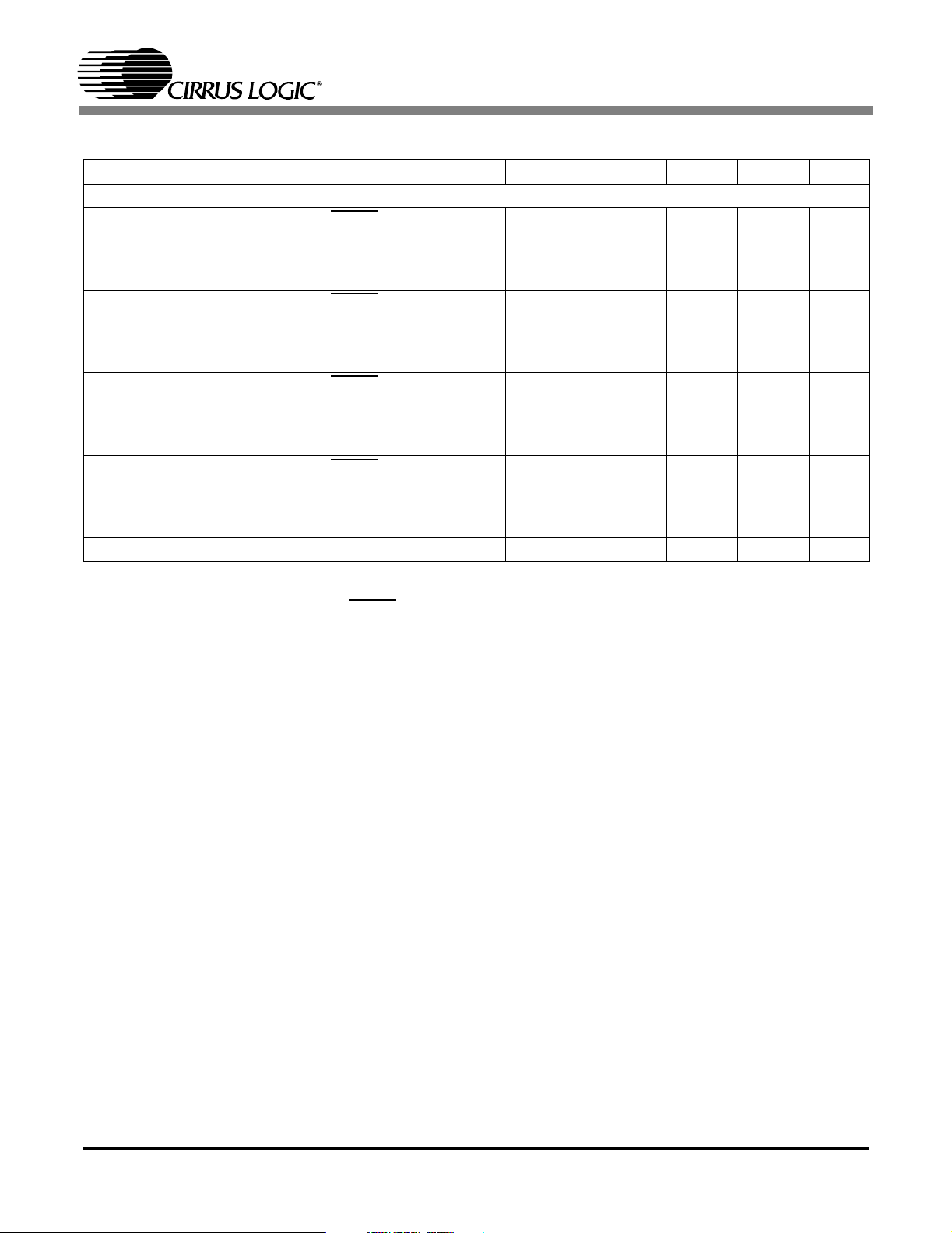
ANALOG CHARACTERISTICS (Continued)
Parameter Symbol Min Typ Max Unit
Power Supplies
CS5180
Power Supply Current (MODE = 1, PWDN
VA1+ , VA 2 + = 5 V
VD1+, VD2+ = 5 V
VD1+, VD2+ = 3 V
Power Supply Current (MODE = 1, PWDN
VA1+ , VA 2 + = 5 V
VD1+, VD2+ = 5 V
VD1+, VD2+ = 3 V
Power Supply Current (MODE = 0, PWDN
VA1+ , VA 2 + = 5 V
VD1+, VD2+ = 5 V
VD1+, VD2+ = 3 V
Power Supply Current (MODE = 0, PWDN
VA1+ , VA 2 + = 5 V
VD1+, VD2+ = 5 V
VD1+, VD2+ = 3 V
Power Supply Rejection (Note 9) PSRR - 55 - dB
Notes: 7. All outputs unloaded. All digital inputs except MCLK held static at VD+ or DGND.
8. Power consumption when PWDN
9. Measured with a 100 mV
=1) (Note7)
-
-
-
=0) (Notes7,8)
-
-
-
=1) (Note7)
-
-
-
=0) (Notes7,8)
= 0 applies only with no master clock applied (MCLK held high or low).
sine wave on the VA+ supplies at a frequency of 100 Hz.
pp
-
-
-
46
92
46
3.7
0.068
0.060
46
15
8.5
3.7
0.068
0.060
55
110
55
6
0.2
0.2
55
20
11.0
6
0.2
0.2
mA
mA
mA
mA
mA
mA
mA
mA
mA
mA
mA
mA
5
Page 6
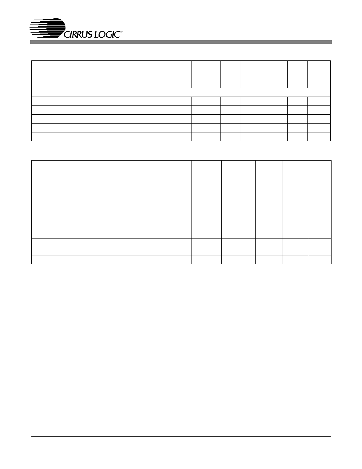
CS5180
DYNAMIC CHARACTERISTICS
Parameter Symbol Min Typ Max Unit
Modulator Sampling Frequency - MCLK - Hz
Output Word Rate - MCLK/64 - Hz
Filter Characteristics (Note 2)
-3 dB Corner - MCLK/142.3804 - Hz
Passband Ripple - - ±0.05 dB
Stopband Frequency - MCLK/128 - Hz
Stopband Rejection 90 - - dB
Group Delay - 2370/MCLK - s
DIGITAL CHARACTERISTICS
(TA=0°Cto70°C;VA+=5V±5%;AGND=DGND=0V)
Parameter Symbol Min Typ Max Unit
High-Level Input Voltage VD+ = 5 V
VD+ = 3 V
Low-Level Input Voltage VD+ = 5 V
VD+ = 3 V
High-Level Output Voltage (I
= -100 µA) VD+ = 5 V
O
VD+ = 3 V
Low-Level Output Voltage (I
= 100 µA) VD+ = 5 V
O
VD+ = 3 V
Input Leakage Current VD+ = 5 V
VD+ = 3 V
Input Capacitance C
V
IH
V
IH
V
IL
V
IL
V
OH
V
OH
V
OL
V
OL
I
in
I
in
in
4.0
2.0
-
-
4
2.7
-
-
-
-
-6-pF
±1
±1
-
-
-
-
-
-
-
-
-
-
0.8
0.8
-
-
0.4
0.3
±10
±10
V
V
V
V
V
V
V
V
µA
µA
6
Page 7
CS5180
SWITCHING CHARACTERISTICS (T
= 0 °C to 70 °C; VA+ = 5 V ±5%, VD+ = 2.7 V to 5.5 V;
A
AGND = DGND = 0 V; MODE = VD+)
Parameter Symbol Min Typ Max Unit
Master Clock Frequency (Note 2) MCLK 0.512 25.6 26 MHz
Master Clock Duty Cycle 45 - 55 %
Rise Times (Notes 2, 10, and 11)
Any Digital Input, Except MCLK
MCLK
Any Digital Output
Fall Times (Notes 2, 10, and 11)
Any Digital Input, Except MCLK
MCLK
Any Digital Output
t
t
rise
fall
-
-
-
-
-
-
20
20
-
-
-
-
100
.2/MCLK
-
100
.2/MCLK
-
ns
s
ns
ns
s
ns
Calibration/Sync
RESET
RESET
rising to MCLK rising
rising recognized, to FSO falling
-3 -ns
- 988205/MCLK - s
SYNC rising to MCLK rising - 3 - ns
SYNC rising recognized to FSO falling - 5161/MCLK - s
PWDN
rising recognized to FSO falling
SYNC high time
RESET
low time
- 5168/MCLK - s
1/MCLK - - s
1/MCLK - - s
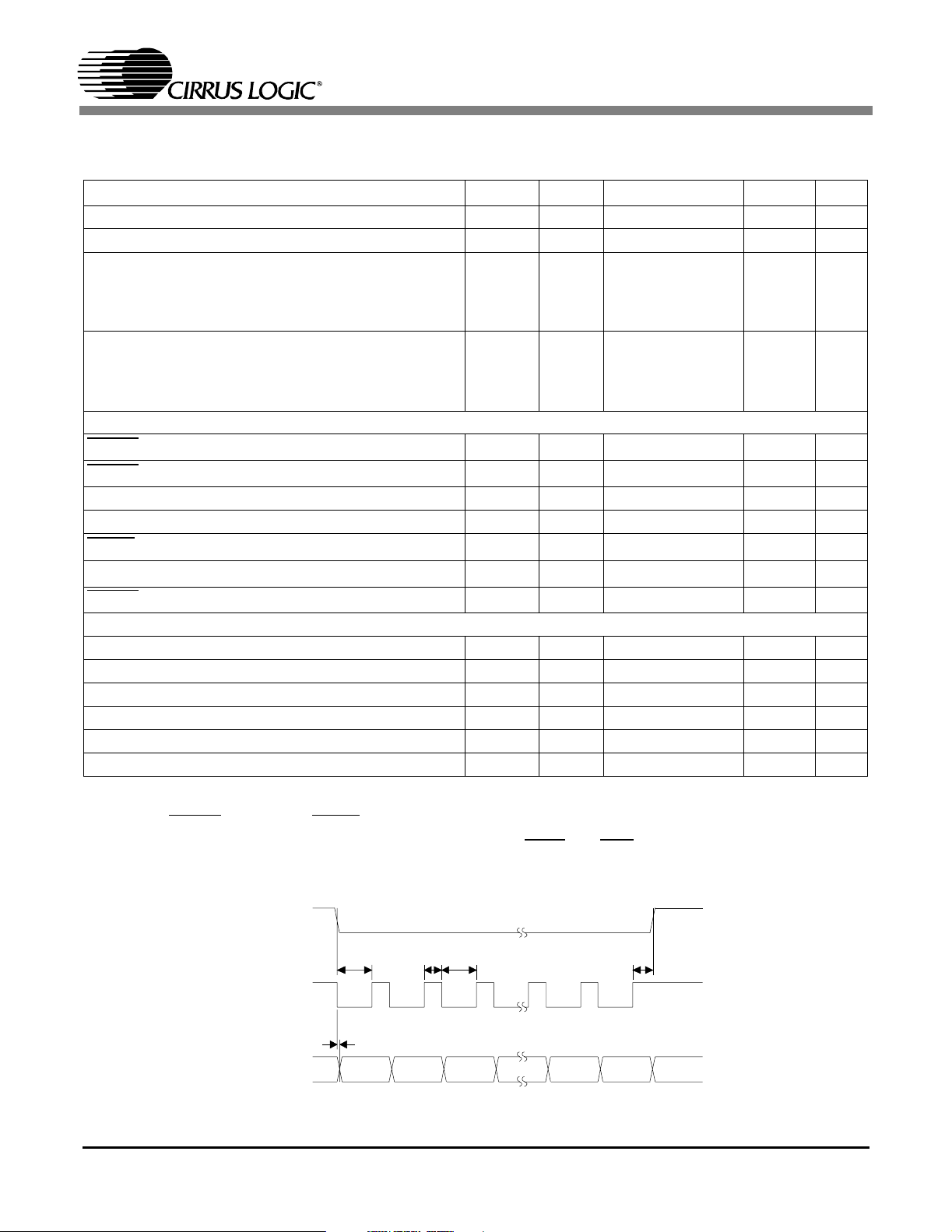
Serial Port Timing (Note 12)
SCLK frequency - MCLK/3 - Hz
SCLK high time t
SCLK low time t
FSO falling to SCLK rising t
SCLK falling to new data bit available t
SCLK rising to FSO rising t
1
2
3
4
5
-1/MCLK -s
-2/MCLK -s
-2/MCLK+2E-9 - s
-1.5 -ns
-1/MCLK-2E-9 - s
Notes: 10. Rise and Fall times are specified at 10% to 90% points on waveform.
11. RESET
12. Specifications applicable to complementary signals SCLK
, SYNC, and PWDN have Schmitt-trigger inputs.
FSO
t1t
2
SCLK
SDATA
t
3
t
4
XX
MSB MSB-1 LSB-1 LSB
and SDO.
Figure 1. Serial Port Timing (not to scale)
t
5
XX
7
Page 8
CS5180
RECOMMENDED OPERATING CONDITIONS (AGND = DGND = 0 V)
Parameter Symbol Min Typ Max Unit
DC Power Supplies Digital
Analog
Analog Reference Voltage VREFIN 2.25 2.5 2.6 V
AGND to DGND Differential -100 0 100 mV
Operating Junction Temperature T
ABSOLUTE MAXIMUM RATINGS
Parameter Symbol Min Max Unit
DC Power Supplies Ground
Digital
Analog
Input Current, Any pin except Supplies I
Output Current I
Power Dissipation (Total) - 1000 mW
Analog Input Voltage and VREFIN voltage V
Digital Input Voltage V
Ambient Operating Temperature T
Storage Temperature T
VD+
VA+
j
AGND/DGND
VD+
VA+
in
out
INA
IND
A
stg
2.7
4.75
- - 120 °C
3
5
-0.3
-0.3
-0.3
-±10mA
-±25mA
-0.3 (VA+) + 0.3 V
-0.3 (VD+) + 0.3 V
070°C
-65 150 °C
5.5
5.25
0.3
6.0
6.0
V
V
V
V
V
WARNING: Operation beyond these limits may result in permanent damage to the device. Normal operation is not
guaranteed at these extremes.
8
Page 9
CS5180
GENERAL DESCRIPTION
The CS5180 is a monolithic CMOS 16-bit A/D
converter designed to operate in a continuous mode
after being reset.
The CS5180 can operate in a modulator-only mode
in which the unfiltered bit stream from the modulator is the data output from the device.
THEORY OF OPERATION
The front page of this data sheet illustrates the
block diagram of the CS5180.
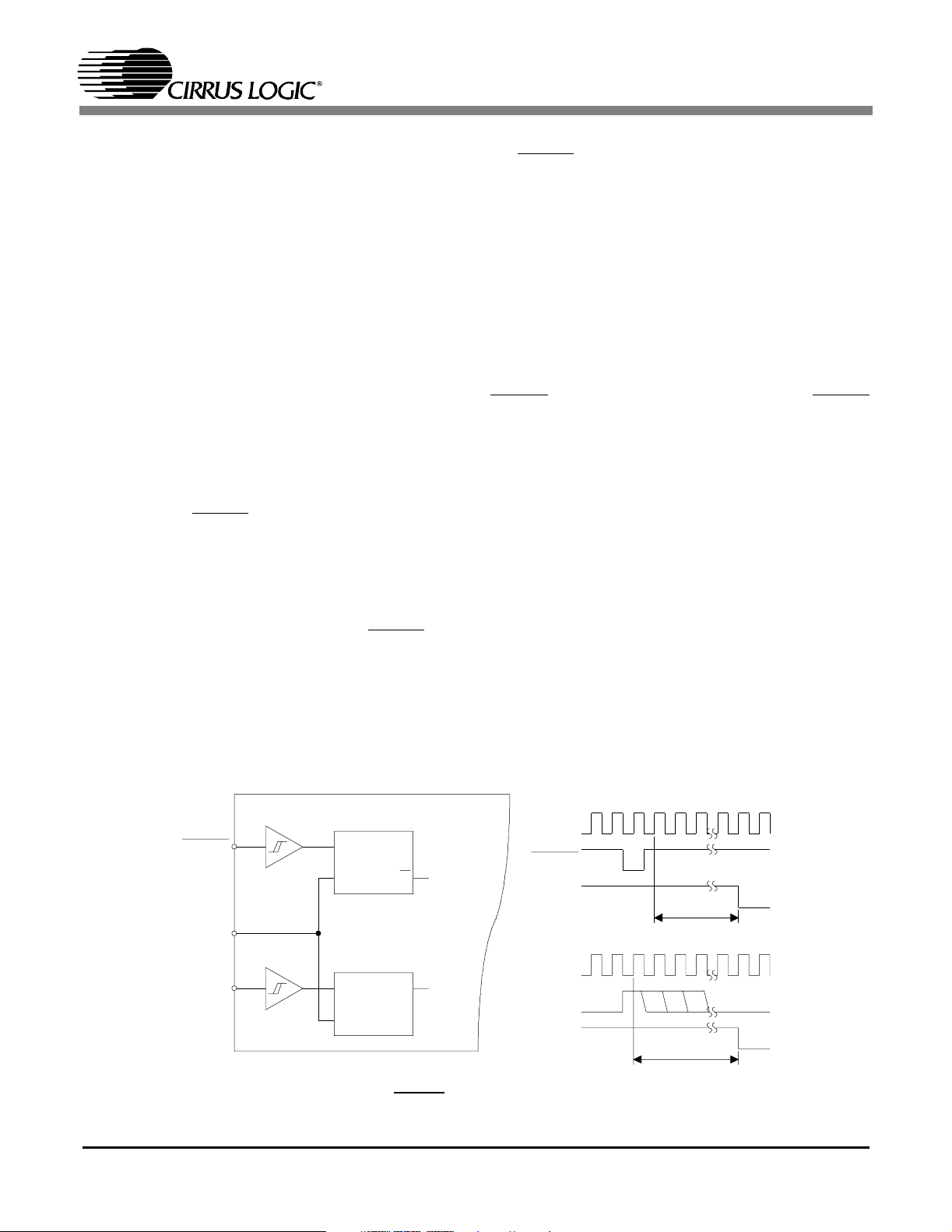
Converter Initialization: Calibration and Synchronization
The CS5180 does not have an internal power-on reset circuit. Therefore when power is first applied to
the device the RESET
power is established and the voltage reference has
stabilized. This resets the converter’s logic to a
known state. When power is fully established the
converter will perform a self-calibration, starting
with the first MCLK rising edge after RESET
high. The converter will use 988,205 MCLK cycles
to complete the calibration and to allow the digital
filter to fully settle, after which, it will output fullysettled conversion words. The converter will then
continue to output conversion words at an output
pin should be held low until
goes
word rate equal to MCLK/64. Figure 2 illustrates
the RESET
and SYNC logic and timing for the con-
verter.
The CS5180 is designed to perform conversions
continuously with an output rate that is equivalent
to MCLK/64. The conversions are performed and
the serial port is updated independent of external
controls. The converter is designed to measure differential bipolar input signals, and unipolar signals,
with a common mode voltage of between 1.0 V and
VREF + 0.25 V. Calibration is performed when the
RESET
signal to the device is released. If RESET
is properly framed to MCLK, the converter can be
synchronized to a specific MCLK cycle at the system level.
The SYNC signal can also be used to synchronize
multiple converters in a system. When SYNC is
used, the converter does not perform calibration.
The SYNC signal is recognized on the first rising
edge of MCLK after SYNC goes high. SYNC
aligns the output conversion to occur every 64
MCLK clock cycles after the SYNC signal is recognized and the filter is settled. After the SYNC is
initiated by going high, the converter will wait
5,161 MCLK cycles for the digital filter to settle
before putting out a fully-settled conversion word.
To synchronize multiple converters in a system, the
RESET
MCLK
SYNC
CS5180
D
CLK
D
CLK
Figure 2. RESET and SYNC logic and timing.
Q
Q RESET
QSYNC
MCLK
RESET
FSO
988205 MCLK Cycles
MCLK
SYNC
FSO
5161 MCLK Cycles
9
Page 10

CS5180
SYNC pulse should rise on a falling edge of the
MCLK signal. This ensures that the SYNC input to
all CS5180s in the system will be recognized on the
next rising edge of MCLK. Use of the SYNC input
is not necessary to make the converter operate
properly. If it is unused it should be tied to DGND.
Conversion data is output from the SDO and SDO
pins of the device. The data is output from the SDO
pin MSB first, in two’s complement format. The
converter furnishes a serial clock SCLK and its
complement SCLK
to latch the data bits; and a data
framing signal, Frame Sync Output (FSO), which
frames the output conversion word. The SCLK
output frequency is MCLK/3.
Clock Generator
The CS5180 must be driven from a CMOS-compatible clock at its MCLK pin. The MCLK input is
powered from the VD+ supply and its signal input
should not exceed this supply. The required
MCLK is 64 × OWR (Output Word Rate). To
achieve an Output Word Rate of 400 kHz, the
MCLK frequency must be 64 × 400 kHz, or
25.6 MHz. A second clock input pin, MCLK
not actually used inside the device but allows the
user to run a fully differential clock to the converter
,is
to minimize radiated noise from the PC board layout.
The CS5180 can be operated with MCLK frequencies from 512 kHz up to 26 MHz. The output word
rate scales with the MCLK rate with
OWR = MCLK/64.
Voltage Reference
The CS5180 can be configured to operate from either its internal voltage reference, or from an external voltage reference.
The on-chip voltage reference is 2.375 V and is referenced to the AGND pin. This 2.375 V reference is
output from the VREFOUT pin. It is then filtered
andreturnedtotheVREFINpin.VREFINpinis
connected to a buffer which has a gain of 1.6. This
scales the on-chip reference of 2.375 V to 3.8 V.
This value sets the peak-to-peak input voltage into
the AIN pins of the converter. Figure 3 illustrates the
CS5180 connected to use the internal voltage reference. Note that a 1.0 µF and 0.1 µF capacitor are
shown connected to the VREFCAP pin to filter out
noise. A larger capacitor can be used, but may require a longer reset period when first applying power
to the part to allow for the reference to charge up the
capacitors and stabilize before self-calibration begins.
10
CS5180
VREFIN
VREF+
10 µF 0.1 µF
+
+
10 µF 0.1 µF
+
1µF 0.1µF
Figure 3. CS5180 connection diagram for using the internal voltage reference.
VREF-
VREFOUT
VREFCAP
X1.6
Modulator
X1
Reference
Page 11

CS5180
VS
+
10 µF 0.1 µF
Figure 4. CS5180 connection diagram for using an external voltage reference.
2.5 V
10 µF
0.1 µF
+
10 µF 0.1 µF
10 µF 0.1 µF
1µF 0.1µF
Alternatively, the CS5180 can be configured to use
an external voltage reference. Figure 4 illustrates
the CS5180 connected to use a 2.5 V external reference. In this case, the peak-to-peak input at the
AINpinsis4V.
Analog Input
The analog signal to the converter is input into the
AIN+ and AIN- pins. The input signal is fully differential with the maximum peak-to-peak amplitude of VREFIN X 1.6 V. The signal needs to have
a common mode voltage in a range from 1 V to
VREF + 0.25 V. A resistor-capacitor filter should
be included on the AIN+ and AIN- inputs of the
converter. This should consist of a 20 Ω resistor
and a 2200 pF capacitor on each input to ground as
illustrated in the system connection diagram (Figure ).
Output Coding
Table 1 illustrates the output coding for the converter when operating with the digital filter
(MODE = 1). The converter outputs its data from
the serial port in twos complement format, MSB
first.
CS5180
VREFIN
VREF+
+
VREF-
VREFOUT
+
VREFCAP
+
Fully Differential Bipolar
Input Voltage
- 1.5 LSB) 7FFF
>(V
FS
-1.5LSB
V
FS
-0.5 LSB
-VFS+0.5LSB
<(-VFS+ 0.5 LSB) 8000
Notes: 1. V
X1.6
Modulator
X1
Reference
1
=VREFINx1.6
FS
Table 1. Output Coding.
Twos Complement
7FFF
7FFE
0000
FFFF
8001
8000
The chip offers an MFLAG signal to indicate when
the modulator has gone unstable. MFLAG is set
when an overrange signal forces the modulator into
an unstable condition. Under this condition, output
codes from the converter will be locked to either
plus or minus full scale as is appropriate for the
overrange condition.
Modulator-Only mode
The CS5180 can be operated in modulator-only
mode by connecting the MODE pin to a logic 0
(DGND).
In modulator-only mode the noise-shaped bitstream from the fifth-order delta-sigma modulator
is output from the SDO and SDO
stream) pins.
(inverse bit-
11
Page 12

MCLK
Modulator
Data
SDO
SDO
Reconstructed
Dat a
CS5180
Figure 5. Modulator Only Mode Data RTZ Format.
The data from the modulator is output from
SDO/SDO
in RTZ (Return to Zero) format. The
circuit in Figure 6 can be used to reconstruct the
data so it can be captured with the rising or falling
edge of MCLK.
Table 2 illustrates the magnitude of the input signal
into the chip versus the ones density out of the
modulator. The table does not take into account the
potential offset and gain errors of the modulator
and their effect on the ones density.
Fully Differential Bipolar
Input Voltage
V
FS
0 50%
-V
Notes: 2. V
3. Ones density is approximate; it does not
take offset and gain errors into
consideration.
Table 2. Modulator-Only Mode Ones Density.
2
FS
=VREFINx1.6
FS
Modulator Ones
Density
3
75%
25%
Figure 7 and Figure 8 illustrate magnitude versus
frequency plots of the modulator bitstream when
running at 25.6 MHz.
Figure 7. Magnitude versus frequency spectrum of
modulator bitstream
(MCLK = 25.6 MHz).
12
SDO
SDO
Figure 6. Circuit to Reconstruct
Return-to-Zero (RTZ) Data from
SDO/SDO
into Original Modulator Bitstream.
Reconstructed
Data
Reconstructed
Data
Figure 8. Expanded view of the magnitude versus fre-
quency spectrum of modulator bitstream
Page 13

Instability Indicator
The MFLAG signal is functional in both modes of
operation of the part and indicates when the modulator has been overdriven into an unstable condition. In the modulator only mode (MODE = 0), the
MFLAG signal will remain set for 3 MCLK cycles
when the modulator goes unstable, before being returned to the reset state. While the input condition
causing modulator instability persists, the MFLAG
signal will continually get set for 3 MCLK cycles
and then get reset.
CS5180
When the decimation filter on the part is operational (MODE = 1), the MFLAG signal is set when the
modulator goes unstable. In this mode, however,
the MFLAG signal stays set until 5,120 MCLK cycles after the input condition causing modulator instability is removed. This delay is provided to
allow the digital filter time to settle, and the part
will output fully settled conversion words after the
MFLAG signal goes low.
Digital Filter Characteristics
Figure 9 illustrates the magnitude versus frequency
plot of the converter when operating at 400 kHz
output word rate. The filter is a non-aliasing 4265
tap filter with a -3 dB corner at 0.4495 of the output
word rate and an out-of-band attenuation of at least
90 dB at frequencies above one half the output
word rate. The passband ripple is less than
±0.05 dB up to the -3 dB corner frequency.
Figure 10 illustrates the phase response of the digital filter with the converter operating at 400 kHz
output word rate. The filter characteristics change
proportional to changes in the MCLK rate.
The group delay of the digital filter is 2,370 MCLK
cycles (92.6 µs with MCLK = 25.6 MHz), and the
settling time is 4,740 MCLK cycles (185.2 µs).
Serial Interface
The CS5180 has a serial interface through which
conversion words are output in a synchronous selfclocking format. The serial port consists of the Se-
Figure 9. CS5180 Digital Filter Magnitude Response
(MCLK = 25.6 MHz)
Figure 10. CS5180 Digital Filter Phase Response
(MCLK = 25.6 MHz)
rial Data Output pin (SDO), and its complement
(SDO
); Serial Clock (SCLK), and its complement
(SCLK
); and the Frame Sync Output (FSO). FSO
falls at the beginning of an output word. Data is
output in twos complement format, MSB first.
FSO stays low for 16 SCLK cycles. SCLK is output at a rate equal to MCLK/3.
Power Supplies / Board Layout
The CS5180 can be operated with VA+ supplies at
5 V and VD+ supplies at 5 V; or with VA+ at 5 V
and VD+ at 3 V.
Figure illustrates the system connection diagram
for the chip. For best performance, each of the
13
Page 14

CS5180
supply pins should be bypassed to the nearest
ground pin on the chip. The bypass capacitors
should be located as close to the chip as possible. If
the chip is surface mounted the bypass capacitors
should be on the same side of the circuit card as the
chip.
The CS5180 is a high speed component that requires adherence to standard high-frequency printed circuit board layout techniques to maintain
optimum performance. These include the use of
ground and power planes, using low noise power
supplies in conjunction with proper supply decou-
1
AGND1
+5 V
0.1 µF
28
VA1+
8
VA2+
pling, minimizing circuit trace lengths, and physical separation of digital and analog components
and circuit traces.
It is preferred that any clock oscillator circuitry be
located on a ground plane separate from the digital
plane in order to ensure that digital noise does not
induce clock jitter.
For additional insight, see the CDB5180 evaluation
board for more details. Also refer to Application
Note AN18 about layout and design rules for data
converters.
22
21
12
0.1 µF
+5 V o r
+3. 0 V
CS5180
DGND1
VD1+
VD2+
3.8 V Fully
pp
Differential
CMV = 2. 375 V
10 µF
10 µF
1µF
~
0.1 µF
+
0.1 µF
+
0.1 µF
+
0.1 µF
Ω
20
2200 pF
Ω
20
2200 pF
7
18
4
5
3
2
6
26
27
AGND2
AGND3
VREFOUT
VREFIN
VREF-
VREF+
VREFCAP
AIN+
AIN-
DGND2
PWDN
MODE
RESET
SYNC
MFLAG
MCLK
MCLK
FSO
SCLK
SCLK
SDO
SDO
11
25
24
23
10
9
20
19
17
14
13
16
15
0.1 µF
Control
Logic
Clock
Source
Data
Interface
†
The 3.8 Vpp fully differential input span is set by the converter’s internal voltage reference at 2.375 V.
An input span of 4.0 Vpp fully differential would result if an external voltage reference of 2.5 V is used.
† Miniature surface mount 25.6 MHz clock oscillators may be ordered from the CTS Reeves Company.
For 4.5 V to 5.5 Volt Operation, order P/N 974-7725-0000A
For 3.0 to 3.6 Volt Operation, order P/N 974-7727-0000A
14
Figure 11. CS5180 System Connection Diagram
Page 15

CS5180
Power-down Mode
The CS5180 has a PWDN (power-down) function.
When active low, power to most of the converter’s
circuitry will be reduced. If MCLK is to be stopped
to save power, it should not be stopped until at least
ten clock cycles after PWDN is taken low. The ten
clock cycles are required to allow the part to turn
off it’s internal circuitry. If the part does not get the
full ten clock cycles, it will still go into a power
down state, but the power dissipation could be
more than is listed in the specifications for the full
power down condition. When PWDN
calibration information inside of the converter is
maintained. When coming out of the power-down
state, the converter is not recalibrated and will
start-up similar to when SYNC is initiated.
is active, the
15
Page 16

PIN DESCRIPTION
Analog Ground AGND
Pos. Reference VREF+ VA1+ Positive Analog Supply
Neg. Reference VREF- AIN- Negative Analog Input
Reference Output VREFOUT AIN+ Positive Analog Input
Pos. Reference Input VREFIN PWDN
Reference Bypass VREFCAP MODE Modulator Only Mode
Analog Ground AGND RESET
Analog Supply VA2+ DGND Digital Ground
Invalid Conversion MFLAG VD1+ Positive Digital Supply
Sync. Filter SYNC MCLK Master Clock
Digital Ground DGND MCLK
Pos. Digital Supply VD2+ AGND Analog Ground
Inverse Serial Clock SCLK
Serial Clock SCLK SDO Serial Data Out
5
6
7
8
9
10
11
12 13 14 15 16 17
1234282726
CS5180
18
25
24
23
22
21
20
19
FSO Frame Sync Output
SDO
Power Down Mode
Reset and Calibration
Inverse Master Clock
Inverse Serial Data Out\
CS5180
Supply Inputs
VA1+, VA2+ — Positive Analog Supply
Input for positive analog supply is +5 V typical when AGND is 0 V.
AGND — Analog Ground
Analog ground for circuits supplied by VA+.
VD1+, VD2+ — Positive Digital Supply
Input for positive digital supply is +5 V typical when DGND is 0 V.
DGND — Digital Ground
Digital ground for circuits supplied by VD+.
Signal and Reference Related Inputs
AIN+, AIN- — Differential Analog Inputs
Fully differential signal inputs.
VREFIN — Voltage Reference Input
16
VREFOUT or an external reference is connected to VREFIN. Analog input voltage (full scale
fully differential peak-to-peak) into the converter is 1.6 times this value.
Page 17

VREF+ — Positive Voltage Reference
Filter capacitor connection for the reference input buffer. The voltage on this pin equals
VREFINX1.6.
VREF- — Negative Voltage Reference
VREF- is connected to AGND.
VREFOUT — Voltage Reference Output
Output pin for the 2.375 volt on-chip reference relative to AGND.
VREFCAP — Reference Bypass
Filter capacitor connection for the internal reference.
Serial Interface I/O Signals
SCLK, SCLK — Serial Interface Clock
Serial Clock Output. A gated serial clock output from the converter at a rate equal to 1/3 the
MCLK clock rate. The SCLK
if the two lines are run adjacent on the PC board layout.
output is a complement of SCLK and helps reduce radiated noise
CS5180
SDO, SDO
FSO — Frame Sync Output
Control Pins
RESET — Reset and Calibration
PWDN
—SerialDataOut
Serial Data Output. Output pin for 16-bit serial data word. The SDO output is the complement
of SDO and helps to reduce radiated noise if the two lines are run adjacent on the PC board
layout. Output data is output in twos complement format MSB first.
The Frame Sync Output indicates the beginning of an output word from the SDO pin by falling
to a logic low state. FSO remains low until all 16 bits are clocked out.
When the RESET pin is pulled to a logic low the converter will perform a reset of its digital
logic. When the level on this pin is brought back to a logic high the chip starts normal
operation, following a two clock cycle delay period. When MODE = 1 the chip goes through
an internal gain and offset calibration routine following this reset sequence.
— Power Down Mode
A logic 0 on PWDN pin will put the device into a power-down mode.
17
Page 18

MODE — Modulator Mode
MODE is held at a logic high for normal operation. In normal operation the device utilizes the
digital decimation filter and calibration circuitry. MODE = 0 puts the part in modulator-only
mode whereby most of the digital circuitry is powered-down and the modulator bit-stream is
output from the SDO and SDO pins.
SYNC — Synchronization of Filter
The SYNC input can be used to restart the digital filter of the converter at the beginning of its
convolution cycle. The SYNC input is used to synchronize the filters of multiple converters in
a system. When the SYNC pin goes high, the filter will be initialized and will begin its
convolution cycle on the next rising edge of MCLK. If not used, tie sync to DGND.
MFLAG — Invalid Conversion Flag
MFLAG goes high if the modulator portion of the converter goes unstable. If MFLAG is high,
the output data from the converter may be invalid.
CS5180
MCLK, MCLK
Master clock input accepts a CMOS level clock input to the converter with worst case duty
cycle of 45-55% (typically 25.6 MHz). MCLK
be used for radiated noise cancellation if MCLK and MCLK
the PC board.
— Master Clock Signal
is not actually used inside the device, but can
are run adjacent to each other on
18
Page 19

PARAMETER DEFINITIONS
Differential Non-Linearity Error - DNL
The deviation of a code’s width from ideal. Units in LSBs.
Integral Non-Linearity Error - INL
The deviation of a code from a straight line passing through the endpoints of the transfer
function after zero- and full-scale errors have been accounted for. "Zero-scale" is a point 1/2
LSB below the first code transition and "full-scale" is a point 1/2 LSB beyond the code
transition to all ones. The deviation is measured from the middle of each particular code. Units
in LSB’s.
Full-Scale Error - FSEP
The deviation of the last code transition from the ideal (VREF-3/2 LSB’s). Units in LSB’s.
Offset Error - VOS
The deviation of the mid-scale transition from the ideal (1/2 LSB below 0 Volts). Units in
LSB’s.
CS5180
Spurious-Free-Dynamic-Range - SFDR
The ratio of the rms value of the full-scale signal, to the rms value of the next largest spectral
component (excepting dc). This component is often an aliased harmonic when the signal
frequency is a significant proportion of the sampling rate. Units in dBc (decibels relative to the
carrier).
Total Harmonic Distortion - THD
The ratio of the rms sum of the significant harmonics (2nd through 7th), to the rms value of the
full-scale signal. Units in decibels.
Dynamic Range - DR
The ratio of the rms value of the inferred full-scale signal, to the rms sum of the broadband
noise signals below the Nyquist rate (excepting dc and distortion terms). Expressed in
decibels. Dynamic Range is tested with a 22 kHz input signal 60 dB below full scale. 60 dB
is then added to the resulting number to refer the noise level to the full-scale signal. This
technique ensures that the distortion components are below the noise level and do not affect the
measurement.
Signal-to-Noise-and-Distortion (s/[n+d]) - SINAD
The ratio of the rms value of the full-scale signal, to the rms sum of all other spectral
components below the Nyquist rate (excepting dc), including distortion components. Expressed
in decibels.
Group Delay
The time delay through the digital filter section of the part. Units in seconds.
19
Page 20

Resolution - N
The number of different output codes possible. Expressed as N, where 2
available output codes.
Noise -
A measure of the variability of the converter’s output when a fixed DC input (usually ground)
is applied to the input and a large number of samples are taken. RMS noise is determined
statistically as the Standard Deviation of the Probability Density Function derived from the
histogram of the ADC with the differential inputs shorted together and tied to an appropriate
common mode voltage.
Common Mode Rejection Ratio - CMRR
A measure of the device’s ability to cancel out the effect of a common voltage applied to both
of its differential inputs. CMRR is specified as the ratio of the differential signal gain to the
gain for the common-mode signal. Units in dB.
Offset Drift -
Changes in the offset error of the part after self calibration due to changes in ambient
temperature. Specified in microvolts per degree C, relative to the input signal.
CS5180
N
is the number of
Full Scale Drift -
Changes in the full scale error of the part after self calibration due to changes in ambient
temperature. Specified in parts-per-million (PPM) of the full scale range per degree C.
20
Page 21

+15
0.1 µF
0.15
C0G
+
10 k
Ω
10 k
5k
Figure 12. Single amplifier driving only AIN+, AIN- held at steady dc value
-
U1
+
Ω
Ω
-15
10 µF
++
APPENDIX A: CIRCUIT APPLICATIONS
Several amplifier circuits have been tested with the
CS5180. Performance at higher frequencies is generally limited by the operational amplifiers used to
drive the A/D converter.
1k
Ω
0.1 µF
20
Ω
2200 pF
Ω
20
2200 pF
CS5180
AIN+
CS5180
AIN-
VREFOUT
10 µF0.1 µF
Figure 12 illustrates a single operational amplifier
circuit which can accept a single-ended ground-referenced signal and condition it for the input of the
CS5180. The amplifier is AC-coupled to the signal
source. In this circuit the AIN- input to the CS5180
is held at a constant DC value and the AIN+ input
is driven (it is actually overdriven to achieve high
dynamic range, but this sacrifices performance
with regard to distortion). The common mode voltage for the CS5180 input should be designed to
stay between 1 V and VREF + 0.25 V when driven
at its AIN+ and AIN- inputs. In Figure 12 the dc
voltage at the AIN- input is set so that when driven
with a 4 V
signal on the AIN+ pin, the common
pp
mode voltage remains within the proper range.
Figures 13 and 14 illustrate the performance of the
amplifier of Figure 12 operating with a 4 V
into the AIN+ input; and with 2 V
input into the
pp
pp
input
AIN+ input respectively.
Figure 13. Performance of amplifier of Figure 12 over-
driving AIN+ input to the CS5180 at 4 V
PP
Figure 15 illustrates an AC-coupled two amplifier
circuit. This circuit gives better performance than
Figure 14. Performance of amplifier of Figure 12 with
AIN+ driven at 2 V
PP
21
Page 22

20 µF
10 k
CS5180
Ω
2k
+15
Ω
2k
+
Ω
2k
0.1 µF
-
U1
+
-15
Ω
0.1 µF
Ω
2k
+15
0.1 µF
-
U2
+
Ω
400
2200 pF
2200 pF
400
100
Ω
AIN-
CS5180
Ω
AIN+
-15
0.1 µF 10 µF
Figure 15. AC-coupled driver using two amplifiers.
the single amplifier circuit of Figure 12 because the
inputs to the CS5180 are driven differentially. The
400 and 100 Ω output divider scales down the input
from the amplifier. The scaling should be optimized for the application. Figure 16 illustrates the
performance of the converter when using this amplifier circuit.
The amplifier of Figure 17 uses three amplifiers
and can accept a ground referenced signal or a fully
differential signal. Figure 18 illustrates its performance when driven with 57.6 kHz signal.
Figure 19 illustrates a four amplifier circuit which
gives the best performance by keeping everything
balanced. Performance is generally limited by the
amplifiers. Again, the output resistors are used to
scale down the input signal. Figures 20 and 21 il-
0.1 µF
+
VREFOUT
Figure 16. Performance of amplifier in Figure 15
22
Page 23

XLR
7.77 k
+
10 µF
C0G
CS5180
+12 V
0.1 µF
-
0.1 µF
0.1 µF
U1
+
-12 V
+12 V
-12 V
10 pF
1M
U2
+
0.1 µF
Ω
-
10 k
10 k
Ω
Ω
7.77 k
7.77 k
20 pF
C0G
Ω
Ω
20 pF
C0G
Ω
150
Ω
2200 pF
100
2200 pF
0.1µF 47µF
AIN-
CS5180
Ω
VREFOUT
10 µF
C0G
+
7.77 k
+12 V
20 pF
C0G
Ω
20 pF
C0G
-
+
U3
-12 V
0.1 µF
0.1 µF
150
Ω
AIN+
Figure 17. Three amplifier driver
lustrate the performance of the CS5180 with this
amplifier circuit.
Figure 22 illustrates a Differential Non-linearity
plot of the converter. Data for the plot was taken
using a repeating ramp. Figure 23 is a histogram of
the DNL data in Figure 22.
Figure 24 illustrates a noise histogram of the converter with its inputs shorted and connected to a
proper common mode voltage.
Figure 18. Performance of amplifier in Figure 17
23
Page 24

2k
CS5180
Ω
10 k
2k
+15 V
0.1 µF
U1
+
Ω
-15 V
2k
+15 V
Ω
0.1 µF
-
U2
+
-15 V
0.1 µF
Ω
0.1 µF
10 k
2k
Ω
2k
Ω
Ω
-
+
-15
+15 V
-
+
+15 V
U3
2k
U4
-15 V
10 µF
0.1 µF
0.1 µF
Ω
0.1 µF
+
2200 pF
2200 pF
0.1 µF
301
301
10 k
Ω
AIN-
CS5180
Ω
100
Ω
AIN+
Ω
VREFOUT
Figure 19. Four amplifier driver.
Figure 20. Performance of amplifier in Figure 19
Figure 21. Performance of amplifier in Figure 19
24
Page 25

CS5180
00000000000000000000
00000000000000000000
00000
00000
00000
00000
00000
00000
0000000000000000000000000000
00000
00000
00000
00000
00000
00000
00000
00000
00000
00000
00000
00000
00000
00000
00000
00000
00000
Figure 22. CS5180 Differential Non-linearity plot.
(Data taken with repeating ramp)
50000
40000
30000
20000
Codes
10000
105
0
Figure 23. Histogram of DNL from Figure 22
10684
-0.15
-0.25 to
-0.15 to
42468
000000000000000
000000000000000
000000000000000
000000000000000
000000000000000
-0.05
DNL ( LSB) Ran ge
12085
00000000000000
0.05
-0.05 to
0.15
0.05 to
192
0.15 to
0.25
40000
33885
0000000000000000000000
30000
0000000000000000000000
0000000000000000000000
0000000000000000000000
20000
Count
0000000000000000000000
0000000000000000000000
0000000000000000000000
10000
146
0
FFF6 FFF5 FFF4 FFF3
Figure 24. CS5180 Noise Histogram, > 60,000 samples.
0000000000000000000000
0000000000000000000000
Code (Hexadecimal)
0000000000000000000000
0000000000000000000000
0000000000000000000000
0000000000000000000000
0000000000000000000000
0000000000000000000000
0000000000000000000000
0000000000000000000000
31415
1LSB=61µV
STD = 0.507 LSB
No is e ( r m s ) = 31 µV
88
25
Page 26

PACKAGE OUTLINE DIMENSIONS
28L PLCC PACKAGE DRAWING
CS5180
e
D2/E2
B
D1
D
E1 E
A1
A
INCHES MILLIMETERS
DIM MIN MAX MIN MAX
A 0.165 0.180 4.043 4.572
A1 0.090 0.120 2.205 3.048
B 0.013 0.021 0.319 0.533
D 0.485 0.495 11.883 12.573
D1 0.450 0.456 11.025 11.582
D2 0.390 0.430 9.555 10.922
E 0.485 0.495 11.883 12.573
E1 0.450 0.456 11.025 11.582
E2 0.390 0.430 9.555 10.922
e 0.040 0.060 0.980 1.524
JEDEC # : MS-018
26
Page 27

• Notes •
Page 28

 Loading...