

Page 1

Features
■ V
2
™
Control Topology
■ Dual N Channel Design
■ 100ns Controller Transient
Response
■ Excess of 1Mhz Operation
■ 5 Bit DAC with 1% Tolerance
■ Power Good Output With
Internal Delay
■ Enable Input Provides
Micropower Shutdown Mode
■ Complete Pentium
®
II System
Requires 18 Components
■ 5V and 12V Operation
■ Adaptive Voltage Positioning
■ Remote Sense Capability
■ Current Sharing Capability
■ V
CC
Monitor
■ Hiccup Mode Short Circuit
Protection
■ Overvoltage Protection (OVP)
■ Programmable Soft Start
■ 150ns PWM Blanking
■ 65ns FET Non-Overlap
■ 40ns Gate Rise and Fall Times
(3.3nF load)
Package Options
CS5165
Fast, Precise 5-Bit Synchronous Buck Controller
for the Next Generation Low Voltage Pentium® II Processors
CS5165
Description
The CS5165 synchronous 5-bit NFET
buck controller is optimized to manage
the power of the next generation
Pentium
®
II processors. It’s V
2
™
control
architecture delivers the fastest transient
response (100ns), and best overall voltage
regulation in the industry today. It’s feature rich design gives end users the maximum flexibility to implement the best
price/performance solutions for their end
products.
The CS5165 has been carefully crafted to
maximize performance and protect the
processor during operation. It has a 5-bit
DAC on board that holds a ±1% tolerance
over temperature. Its on board programmable soft start insures a control
start up, and the FET nonoverlap circuitry ensures that both FETs do not conduct
simultaneously.
The on board oscillator can be programmed up to 1MHz to give the designer maximum flexibility in choosing exter-
nal components and setting systems costs.
The CS5165 protects the processor during
potentially catastrophic events like overvoltage (OVP) and short circuit. The OVP
feature is part of the V
2
™
architecture and
does not require any additional components. During short circuit, the controller
pulses the MOSFETs in a “hiccup” mode
(3% duty cycle) until the fault is removed.
With this method, the MOSFETs do not
overheat or self destruct.
The CS5165 is designed for use in both
single processor desktop and multiprocessor workstation and server applications. The CS5165’s current sharing capability allows the designer to build multiple parallel and redundant power solutions for multiprocessor systems.
The CS5165 contains other control and
protection features such as Power Good,
ENABLE, and adaptive voltage positioning. It is available in a 16 lead SOIC wide
body package.
Application Diagram
16 Lead SO WIDE
1
V
ID0
V
ID1
V
ID2
V
ID3
ENABLE
C
OFF
SS
V
ID4
V
FB
COMP
LGnd
PWRGD
GATE(L)
PGnd
GATE(H)
V
CC
V2is a trademark of Switch Power, Inc.
Pentium is a registered trademark of Intel Corporation.
5V to 2.8V @ 14.2A for 300MHz Pentium
®
II
Rev. 6/28/99
Cherry Semiconductor Corporation
2000 South County Trail, East Greenwich, RI 02818
Tel: (401)885-3600 Fax: (401)885-5786
Email: info@cherry-semi.com
Web Site: www.cherry-semi.com
A Company
®
SS
0.1µF
0.1 µF
330pF
COMP
C
OFF
V
V
V
V
V
ID4
ID3
ID2
ID1
ID0
12V
1µF
V
CC
GATE(H)
CS5165
GATE(L)
PGnd
LGnd
V
FB
PWRGD
ENABLE
5V
1200µF/10V x 3
IRL3103
IRL3103
3.3K
1000pF
1.2µH
PCB
trace 6mΩ
1200µF
10V x 5
V
V
PWRGD
ENABLE
V
ID0
V
V
ID2
V
ID3
V
CC
SS
ID1
ID4
Pentium® II
System
1
Page 2

Absolute Maximum Ratings
Pin Symbol Pin Name
V
MAX
V
MIN
I
SOURCE
I
SINK
2
PACKAGE PIN # PIN SYMBOL FUNCTION
Package Pin Description
CS5165
V
CC
IC Power Input 16V -0.3V N/A 1.5A Peak
200mA DC
SS Soft Start Capacitor 6V -0.3V 200µA 10µA
COMP Compensation Capacitor 6V -0.3V 10mA 1mA
V
FB
Voltage Feedback Input 6V -0.3V 10µA 10µA
C
OFF
Off-Time Capacitor 6V -0.3V 1mA 50mA
V
ID0-4
Voltage ID DAC Inputs 6V -0.3V 1mA 10µA
GATE(H) High-Side FET Driver 16V -0.3V 1.5A Peak; 1.5A Peak;
200mA DC 200mA DC
GATE(L) Low-Side FET Driver 16V -0.3V 1.5A Peak; 1.5A Peak;
200mA DC 200mA DC
ENABLE Enable Input 6V -0.3V 100µA 1mA
PWRGD Power-Good Output 6V -0.3V 10µA 30mA
PGnd Power Ground 0V 0V 1.5A Peak N/A
200mA DC
LGnd Logic Ground 0V 0V 100mA N/A
Operating Junction Temperature, TJ . . . . . . . . . . . . . . . . . . . . . . . . . . . . . . . . . . . . . . . . . . . . . . . . . . . . . . . . . . . . 0° to 150°C
Lead Temperature Soldering:
Reflow (SMD styles only) . . . . . . . . . . . . . . . . . . . . . . . . . . . . . . . . . . . . . . . . . . . .60 sec max. above 183°C, 230°C Peak
Storage Temperature Range, TS . . . . . . . . . . . . . . . . . . . . . . . . . . . . . . . . . . . . . . . . . . . . . . . . . . . . . . . . . . . . . −65°C to 150°C
ESD Susceptibility . . . . . . . . . . . . . . . . . . . . . . . . . . . . . . . . . . . . . . . . . . . . . . . . . . . . . . . . . . . . . . . . . . . . . . . . . . . . . . . . . . 2kV
1,2,3,4,6 V
ID0-VID4
Voltage ID DAC inputs. These pins are internally pulled up to 5V if left open.
V
ID4
selects the DAC range. When V
ID4
is high (logic one), the Error Amp ref-
erence range is 2.14V to 3.54V with 100mV increments. When V
ID4
is low (logic
zero), the Error amp reference voltage is 1.34V to 2.09V with 50mV increments.
5 SS Soft Start Pin. A capacitor from this pin to LGnd sets the Soft Start and fault
timing.
7 C
OFF
Off-Time Capacitor Pin. A capacitor from this pin to LGnd sets both the normal and extended off time.
8 ENABLE Output Enable Input. This pin is internally pulled up to 1.8V. A logic Low
( < 0.8V) on this pin disables operation and places the CS5165 into a low current sleep mode.
9 V
CC
Input Power Supply Pin.
10 GATE(H) High Side Switch FET driver pin.
11 PGnd High Current ground for the GATE(H) and GATE(L) pins.
12 GATE(L) Low Side Synchronous FET driver pin.
13 PWRGD Power Good Output. Open collector output drives low when VFBis out of
regulation. Active when ENABLE input is low
14 LGnd Reference ground. All control circuits are referenced to this pin.
15 COMP Error Amp output. PWM Comparator reference input. A capacitor to LGnd
provides Error Amp compensation.
16 V
FB
Error Amp, PWM Comparator, and Low VFBComparator feedback input.
Page 3

CS5165
3
Electrical Characteristics: 0˚C < TA< 70˚C; 0˚C < TJ < 125˚C; 8V < VCC< 14V;
2.8V DAC Code (V
ID4=VID2=VID1=VID0
=1, V
ID3
= 0), C
GATE(H)
= C
GATE(L)
= 3.3nF, C
OFF
= 330pF, CSS= 0.1µF; Unless otherwise stated.
PARAMETER TEST CONDITIONS MIN TYP MAX UNIT
■ V
CC
Supply Current
Operating 1V < VFB< V
DAC
(max on-time) 12 20 mA
No Loads on Gate(H) and Gate(L)
Sleep Mode ENABLE = 0V 300 600 µA
■ VCCMonitor
Start Threshold GATE(H) Switching 3.75 3.95 4.15 V
Stop Threshold GATE(H) not switching 3.65 3.87 4.05 V
Hysteresis Start - Stop 80 mV
■ Error Amplifier
VFBBias Current VFB= 0V 0.1 1.0 µA
COMP Source Current COMP = 1.2V to 3.6V; VFB= 2.7V 15 30 60 µA
COMP CLAMP Voltage VFB= 2.7V, Adjust COMP voltage for 0.85 1.0 1.15 V
Comp current = 50µA
COMP Clamp Current COMP = 0V 0.4 1.0 1.6 mA
COMP Sink Current V
COMP
=1.2V; V
FB
= 3V; VSS> 2.5V 180 400 800 µA
Open Loop Gain Note 1 50 60 dB
Unity Gain Bandwidth Note 1 0.5 2 MHz
PSRR @ 1kHZ Note 1 60 85 dB
■ GATE(H) and GATE(L)
High Voltage at 100mA Measure VCC-GATE 1.2 2.0 V
Low Voltage at 100mA Measure GATE 1.0 1.5 V
Rise Time 1.6V < GATE < (V
CC
- 2.5V) 40 80 ns
Fall Time (V
CC
- 2.5V) > GATE > 1.6V 40 80 ns
GATE(H) to GATE(L) Delay GATE(H) < 2V, GATE(L) > 2V 30 65 100 ns
GATE(L) to GATE(H) Delay GATE(L) < 2V, GATE(H) > 2V 30 65 100 ns
GATE pull-down Resistance to PGnd (note 1) 20 50 115 kΩ
■ Fault Protection
SS Charge Time V
FB
= 0V 1.6 3.3 5.0 ms
SS Pulse Period VFB= 0V 25 100 200 ms
SS Duty Cycle (Charge Time/Period) × 100 1.0 3.3 6.0 %
SS Comp Clamp Voltage VFB= 2.7V, VSS= 0V 0.50 0.95 1.10 V
VFBLow Comparator Increase VFBtill no SS 0.9 1.0 1.1 V
pulsing and normal Off-time.
■ PWM Comparator
Transient Response V
FB
= 1.2 to 5V 500ns after 100 150 ns
GATE(H) (after Blanking time) to
GATE(H) = (VCC- 1V) to 1V
Page 4
CS5165
4
Electrical Characteristics: 0˚C < TA< 70˚C; 0˚C < TJ < 125˚C; 8V < VCC< 14V;
2.8V DAC Code (V
ID4=VID2=VID1=VID0
=1, V
ID3
= 0), C
GATE(H)
= C
GATE(L)
= 3.3nF, C
OFF
= 330pF, CSS= 0.1µF; Unless otherwise stated.
■ Voltage Identification DAC
Accuracy (all codes except 11111) Measure V
FB
= COMP (C
OFF
= 0V) -1 +1 %
V
ID4VID3VID2VID1VID0
25˚C ≤ TJ≤ 125˚C; VCC= 12V
1 0 0 0 0 3.505 3.540 3.575 V
1 0 0 0 1 3.406 3.440 3.474 V
1 0 0 1 0 3.307 3.340 3.373 V
1 0 0 1 1 3.208 3.240 3.272 V
1 0 1 0 0 3.109 3.140 3.171 V
1 0 1 0 1 3.010 3.040 3.070 V
1 0 1 1 0 2.911 2.940 2.969 V
1 0 1 1 1 2.812 2.840 2.868 V
1 1 0 0 0 2.713 2.740 2.767 V
1 1 0 0 1 2.614 2.640 2.666 V
1 1 0 1 0 2.515 2.540 2.565 V
1 1 0 1 1 2.416 2.440 2.464 V
1 1 1 0 0 2.317 2.340 2.363 V
1 1 1 0 1 2.218 2.240 2.262 V
1 1 1 1 0 2.119 2.140 2.161 V
0 0 0 0 0 2.069 2.090 2.111 V
0 0 0 0 1 2.020 2.040 2.060 V
0 0 0 1 0 1.970 1.990 2.010 V
0 0 0 1 1 1.921 1.940 1.959 V
0 0 1 0 0 1.871 1.890 1.909 V
0 0 1 0 1 1.822 1.840 1.858 V
0 0 1 1 0 1.772 1.790 1.808 V
0 0 1 1 1 1.723 1.740 1.757 V
0 1 0 0 0 1.673 1.690 1.707 V
0 1 0 0 1 1.624 1.640 1.656 V
PARAMETER TEST CONDITIONS MIN TYP MAX UNIT
■ PWM Comparator: continued
Minimum Pulse Width Drive VFB1.2 to 5V upon 50 150 250 ns
(Blanking Time) GATE(H) rising edge (> V
CC
-1V),
measure GATE(H ) pulse width
■ C
OFF
Normal Off-Time VFB= 2.7V 1.0 1.6 2.3 µs
Extended Off-Time VSS= VFB= 0V 5.0 8.0 12.0 µs
■ Time-Out Timer
Time-Out Time VFB= 2.7V, Measure
GATE(H ) Pulse Width 10 30 50 µs
Fault Duty Cycle V
FB
= 0V 30 50 70 %
■ Enable Input
ENABLE Threshold GATE(H) Switching 0.8 1.15 1.30 V
Shutdown delay (Note 1) ENABLE-to-GATE(H) < 2V 3 µs
Pull-up Current ENABLE = 0V 3 7 15 µA
Pull-up Voltage No load on ENABLE pin 1.30 1.8 3 V
Input Resistance ENABLE = 5V,
R = (5V-V
PULLUP
)/I
ENABLE
10 20 50 kΩ
Page 5
CS5165
5
PARAMETER TEST CONDITIONS MIN TYP MAX UNIT
THRESHOLD ACCURACY
LOWER THRESHOLD UPPER THRESHOLD
MIN TYP MAX MIN TYP MAX UNIT
% of Nominal DAC Output -12 -8.5 -5 5 8.5 12 %
■ DAC CODE
V
ID4VID3VID2VID1VID0
1 0 0 0 0 3.115 3.239 3.363 3.717 3.841 3.965 V
1 0 0 0 1 3.027 3.148 3.268 3.612 3.732 3.853 V
1 0 0 1 0 2.939 3.056 3.173 3.507 3.624 3.741 V
1 0 0 1 1 2.851 2.965 3.078 3.402 3.515 3.629 V
1 0 1 0 0 2.763 2.873 2.983 3.297 3.407 3.517 V
1 0 1 0 1 2.675 2.782 2.888 3.192 3.298 3.405 V
1 0 1 1 0 2.587 2.690 2.793 3.087 3.190 3.293 V
1 0 1 1 1 2.499 2.599 2.698 2.982 3.081 3.181 V
1 1 0 0 0 2.411 2.507 2.603 2.877 2.973 3.069 V
1 1 0 0 1 2.323 2.416 2.508 2.772 2.864 2.957 V
1 1 0 1 0 2.235 2.324 2.413 2.667 2.756 2.845 V
1 1 0 1 1 2.147 2.233 2.318 2.562 2.647 2.733 V
1 1 1 0 0 2.059 2.141 2.223 2.457 2.539 2.621 V
1 1 1 0 1 1.971 2.050 2.128 2.352 2.430 2.509 V
1 1 1 1 0 1.883 1.958 2.033 2.250 2.322 2.397 V
0 0 0 0 0 1.839 1.912 1.986 2.195 2.268 2.341 V
0 0 0 0 1 1.795 1.867 1.938 2.142 2.213 2.285 V
0 0 0 1 0 1.751 1.821 1.810 2.090 2.159 2.229 V
0 0 0 1 1 1.707 1.775 1.843 2.037 2.105 2.173 V
0 0 1 0 0 1.663 1.729 1.796 1.985 2.051 2.117 V
0 0 1 0 1 1.619 1.684 1.748 1.932 1.996 2.061 V
0 0 1 1 0 1.575 1.638 1.701 1.880 1.942 2.005 V
0 0 1 1 1 1.531 1.592 1.653 1.827 1.888 1.949 V
V
ID4VID3VID2VID1VID0
0 1 0 1 0 1.574 1.590 1.606 V
0 1 0 1 1 1.525 1.540 1.555 V
0 1 1 0 0 1.475 1.490 1.505 V
0 1 1 0 1 1.426 1.440 1.455 V
0 1 1 1 0 1.376 1.390 1.405 V
0 1 1 1 1 1.327 1.340 1.353 V
1 1 1 1 1 1.223 1.247 1.273 V
Input Threshold V
ID4
, V
ID3
, V
ID2
, V
ID1
, V
ID0
1.000 1.250 2.400 V
Input Pull-up Resistance V
ID4
, V
ID3
, V
ID2
, V
ID1
, V
ID0
25 50 100 kΩ
Input Pull-up Voltage 4.85 5.00 5.15 V
■ Power Good Output
Low to High Delay V
FB
= (0.8 × V
DAC
) to V
DAC
30 65 110 µs
High to Low Delay VFB= V
DAC
to (0.8 × V
DAC
) 30 75 120 µs
Output Low Voltage V
FB
= 2.4V, I
PWRGD
= 500µA 0.2 0.3 V
Sink Current Limit V
FB
= 2.4V, PWRGD = 1V 0.5 4.0 15.0 mA
Electrical Characteristics: 0˚C < TA< 70˚C; 0˚C < TJ < 125˚C; 8V < VCC< 14V;
2.8V DAC Code (V
ID4=VID2=VID1=VID0
=1, V
ID3
= 0), C
GATE(H)
= C
GATE(L)
= 3.3nF, C
OFF
= 330pF, CSS= 0.1µF; Unless otherwise stated.
Page 6
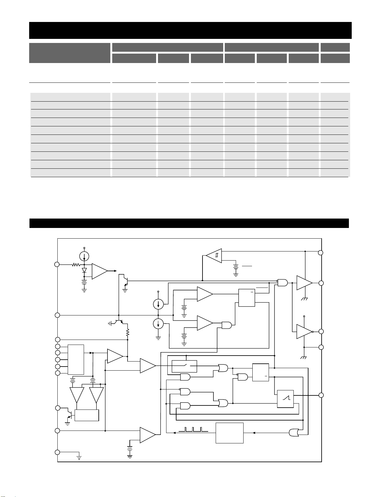
Block Diagram
6
CS5165
THRESHOLD ACCURACY
LOWER THRESHOLD UPPER THRESHOLD
MIN TYP MAX MIN TYP MAX UNITS
% of Nominal DAC Output -12 -8.5 -5 5 8.5 12 %
■ DAC CODE
V
ID4VID3VID2VID1VID0
0 1 0 0 0 1.487 1.546 1.606 1.775 1.834 1.893 V
0 1 0 0 1 1.443 1.501 1.558 1.722 1.779 1.837 V
0 1 0 1 0 1.399 1.455 1.511 1.670 1.725 1.781 V
0 1 0 1 1 1.355 1.409 1.463 1.617 1.671 1.724 V
0 1 1 0 0 1.311 1.363 1.416 1.565 1.617 1.669 V
0 1 1 0 1 1.267 1.318 1.368 1.512 1.562 1.613 V
0 1 1 1 0 1.223 1.272 1.321 1.460 1.508 1.557 V
0 1 1 1 1 1.179 1.226 1.273 1.407 1.454 1.501 V
1 1 1 1 1 1.097 1.141 1.185 1.309 1.353 1.397 V
Note 1: Guaranteed by design, not 100% tested in production.
Electrical Characteristics: 0˚C < TA< 70˚C; 0˚C < TJ < 125˚C; 8V < VCC< 14V;
2.8V DAC Code (V
ID4=VID2=VID1=VID0
=1, V
ID3
= 0), C
GATE(H)
= C
GATE(L)
= 3.3nF, C
OFF
= 330pF, CSS= 0.1µF; Unless otherwise stated.
ENABLE
SS
COMP
V
V
V
V
V
PWRGD
V
FB
LGnd
ID0
ID1
ID2
ID3
ID4
-8.5%
20k
1.25V
5 BIT
DAC
V
CC
+8.5%
-+-
65µs
Delay
7µA
-
+
Enable
Comparator
Error Amplifier
+
-
+
Circuit Bias
1V
60µA
2µA
-
+
PWM
Comparator
-
+
VFB Low
Comparator
Monitor
V
CC
5V
2.5V
PWM Comp
Blanking
0.7V
Off-Time
Extended
Off-Time
Timeout
-
+
+
-
Maximum
On-Time
Timeout
Normal
+
SS Low
Comparator
SS High
Comparator
Time Out
(30µs)
Timer
3.95V
3.87V
R
S
FAULT
Latch
Off-Time
Timeout
FAULT
Q
FAULT
Q
Q
R
S
Q
PWM
Latch
Edge Triggered
V
GATE(H) = ON
GATE(H) = OFF
C
OFF
One Shot
R
S
Q
CC
PGnd
V
CC
V
GATE(H)
V
GATE(L)
PGnd
C
OFF
Page 7

CS5165
7
V
2
™
Control Method
The V
2
™
method of control uses a ramp signal that is generated by the ESR of the output capacitors. This ramp is
proportional to the AC current through the main inductor
and is offset by the value of the DC output voltage. This
control scheme inherently compensates for variation in
either line or load conditions, since the ramp signal is generated from the output voltage itself. This control scheme
differs from traditional techniques such as voltage mode,
which generates an artificial ramp, and current mode,
which generates a ramp from inductor current.
Figure 1: V
2
™
Control Diagram
The V
2
™
control method is illustrated in Figure 1. The output voltage is used to generate both the error signal and
the ramp signal. Since the ramp signal is simply the output
voltage, it is affected by any change in the output regardless of the origin of that change. The ramp signal also contains the DC portion of the output voltage, which allows
the control circuit to drive the main switch to 0% or 100%
duty cycle as required.
A change in line voltage changes the current ramp in the
inductor, affecting the ramp signal, which causes the V
2
™
control scheme to compensate the duty cycle. Since the
change in inductor current modifies the ramp signal, as in
current mode control, the V
2
™
control scheme has the
same advantages in line transient response.
A change in load current will have an affect on the output
voltage, altering the ramp signal. A load step immediately
changes the state of the comparator output, which controls
the main switch. Load transient response is determined
only by the comparator response time and the transition
speed of the main switch. The reaction time to an output
load step has no relation to the crossover frequency of the
error signal loop, as in traditional control methods.
The error signal loop can have a low crossover frequency,
since transient response is handled by the ramp signal
loop. The main purpose of this “slow”feedback loop is to
provide DC accuracy. Noise immunity is significantly
improved, since the error amplifier bandwidth can be
rolled off at a low frequency. Enhanced noise immunity
improves remote sensing of the output voltage, since the
noise associated with long feedback traces can be effectively filtered.
Line and load regulation are drastically improved because
there are two independent voltage loops. A voltage mode
controller relies on a change in the error signal to compensate for a deviation in either line or load voltage. This
change in the error signal causes the output voltage to
change corresponding to the gain of the error amplifier,
which is normally specified as line and load regulation. A
current mode controller maintains fixed error signal under
deviation in the line voltage, since the slope of the ramp
signal changes, but still relies on a change in the error signal for a deviation in load. The V
2
™
method of control
maintains a fixed error signal for both line and load variation, since the ramp signal is affected by both line and load.
Constant Off-Time
To maximize transient response, the CS5165 uses a
Constant Off-Time method to control the rate of output
pulses. During normal operation, the Off-Time of the high
side switch is terminated after a fixed period, set by the
C
OFF
capacitor. To maintain regulation, the V
2
™
Control
Loop varies switch On-Time. The PWM comparator monitors the output voltage ramp, and terminates the switch
On-Time.
Constant Off-Time provides a number of advantages.
Switch duty Cycle can be adjusted from 0 to 100% on a
pulse-by pulse basis when responding to transient conditions. Both 0% and 100% Duty Cycle operation can be
maintained for extended periods of time in response to
Load or Line transients. PWM Slope Compensation to
avoid sub-harmonic oscillations at high duty cycles is
avoided.
Switch On-Time is limited by an internal 30µs (typical)
timer, minimizing stress to the Power Components.
Programmable Output
The CS5165 is designed to provide two methods for programming the output voltage of the power supply. A five
bit on board digital to analog converter (DAC) is used to
program the output voltage within two different ranges.
The first range is 2.14V to 3.54V in 100mV steps, the second
is 1.34V to 2.09V in 50mV steps, depending on the digital
input code. If all five bits are left open, the CS5165 enters
adjust mode. In adjust mode, the designer can choose any
output voltage by using resistor divider feedback to the
VFBpin, as in traditional controllers. The CS5165 is specifically designed to meet or exceed Intel’s Pentium® II specifications.
Start-up
Until the voltage on the V
CC
Supply pin exceeds the 3.95V
monitor threshold, the Soft Start and Gate pins are held
low. The Fault latch is Reset (no Fault condition). The output of the Error Amp (COMP) is pulled up to 1V by the
Comp Clamp. When the V
CC
pin exceeds the monitor
Theory Of Operation
Application Information
COMP
PWM
Comparator
+
C
–
Ramp Signal
Error
Signal
Error
Amplifier
GATE(H)
GATE(L)
E
Output
Voltage
Feedback
–
+
Reference
Voltage
Page 8

threshold, the GateH output is activated, and the Soft Start
Capacitor begins charging. The GateH output will remain
on, enabling the NFET switch, until terminated by either
the PWM Comparator, or the Maximum On-Time Timer.
If the Maximum On-Time is exceeded before the regulator
output voltage achieves the 1V level, the pulse is terminated. The GateH pin drives low, and the GateL pin drives
high for the duration of the Extended Off-Time. This time
is set by the Time-out Timer and is approximately equal to
the Maximum On-Time, resulting in a 50% Duty Cycle. The
GateL Pin will then drive low, the GateH pin will drive
high, and the cycle repeats.
When regulator output voltage achieves the 1V level present at the Comp pin, regulation has been achieved and
normal Off-Time will ensue. The PWM comparator terminates the switch On-Time, with Off-Time set by the C
OFF
Capacitor. The V
2
™
control loop will adjust switch Duty
Cycle as required to ensure the regulator output voltage
tracks the output of the Error Amp.
The Soft Start and Comp capacitors will charge to their
final levels, providing a controlled turn-on of the regulator
output. Regulator turn-on time is determined by the Comp
capacitor charging to its final value. Its voltage is limited
by the Soft Start Comp clamp and the voltage on the Soft
start pin.
Power Supply Sequencing
The CS5165 offers inherent protection from undefined
start-up conditions, regardless of the 12V and 5V supply
power-up sequencing. The turn-on slew rates of the 12V
and 5V power supplies can be varied over wide ranges
without affecting the output voltage or causing detrimental
effects to the buck regulator.
Figure 2: Demonstration board start up in response to increasing 12V
and 5V input voltages. Extended off time is followed by normal off
time operation when output voltage achieves regulation to the error
amplifier output.
Figure 3: Demonstration board start up waveforms.
Figure 4: Demonstration board enable start up waveforms.
Normal Operation
During Normal operation, Switch Off-Time is constant and
set by the C
OFF
capacitor. Switch On-Time is adjusted by
the V
2
™
Control loop to maintain regulation. This results
in changes in regulator switching frequency, duty cycle,
and output ripple in response to changes in load and line.
Output voltage ripple will be determined by inductor ripple current and the ESR of the output capacitors (see figures 5 & 6 ).
CS5165
8
Application Information: continued
Trace 1 Soft Start pin (2V/div)
Trace 2 COMP pin (error amplifier output) (1V/div)
Trace 4 Regulator output voltage (1V/div)
Trace 1 - Regulator Output Voltage (1V/div.)
Trace 2 - Inductor Switching Node (2V/div.)
Trace 3 - 12V input (V
Trace 4 - 5V Input (1V/div.)
) (5V/div.)
CC
Trace 1 - Regulator Output Voltage (1V/div.)
Trace 2 - Inductor Switching Node (5V/div.)
Page 9

Figure 5: Normal Operation showing Output Inductor Ripple Current
and Output Voltage Ripple, 0.5A Load, V
OUT
= +2.84V (DAC = 10111)
Figure 6: Normal Operation showing Output Inductor Ripple Current
and Output Voltage Ripple, I
LOAD
= 14A, V
OUT
= +2.84V (DAC = 10111)
Transient Response
The CS5165 V
2
™
Control Loop’s 100ns reaction time provides unprecedented transient response to changes in
input voltage or output current. Pulse-by-pulse adjustment
of duty cycle is provided to quickly ramp the inductor current to the required level. Since the inductor current cannot
be changed instantaneously, regulation is maintained by
the output capacitor(s) during the time required to slew the
inductor current.
Overall load transient response is further improved
through a feature called “Adaptive Voltage Positioning”.
This technique pre-positions the output capacitors voltage
to reduce total output voltage excursions during changes in
load.
Holding tolerance to 1% allows the error amplifiers reference voltage to be targeted +40mV high without compromising DC accuracy. A “Droop Resistor”, implemented
through a PC board trace, connects the Error Amps feedback pin (V
FB
) to the output capacitors and load and carries
the output current. With no load, there is no DC drop
across this resistor, producing an output voltage tracking
the Error amps, including the +40mV offset. When the full
load current is delivered, an 80mV drop is developed
across this resistor. This results in output voltage being offset -40mV low.
The result of Adaptive Voltage Positioning is that additional margin is provided for a load transient before reaching
the output voltage specification limits. When load current
suddenly increases from its minimum level, the output
capacitor is pre-positioned +40mV. Conversely, when load
current suddenly decreases from its maximum level, the
output capacitor is pre-positioned -40mV (see figures 7, 8,
and 9). For best Transient Response, a combination of a
number of high frequency and bulk output capacitors are
usually used.
If the Maximum On-Time is exceeded while responding to
a sudden increase in Load current, a normal off-time
occurs to prevent saturation of the output inductor.
Figure 7: Output Voltage Transient Response to a 14A load pulse,
V
OUT
= +2.84V (DAC = 10111).
CS5165
9
Application Information: continued
Trace 1 GATE (H) (10V/div)
Trace 2 Inductor Switching Node (5V/div)
Trace 3 Output Inductor Ripple Current (2A/div)
Trace 4 V
Trace 1 - GATE(H) (10/div)
Trace 2 - Inductor Switching Node (5V/div)
Trace 3 - Output Inductor Ripple Current (2A/div)
Trace 4 - V
ripple (20mV/div)
OUT
ripple (20mV/div)
OUT
Trace 3 -Load Current (5A/10mV/div)
Trace 4 - V
OUT
(100mV/div)
Page 10

Figure 8: Output Voltage Transient Response to a 14A load step, V
OUT
=
+2.84V(DAC = 10111).
Figure 9: Output Voltage Transient Response to a 14A load turn-off,
V
OUT
= +2.84V (DAC = 10111).
Short Circuit Protection
A lossless hiccup mode short circuit protection feature is
provided, requiring only the Soft Start capacitor to implement. If a short circuit condition occurs the VFBlow comparator sets the FAULT latch. This causes the top FET to
shut off, disconnecting the regulator from its input voltage.
The Soft Start capacitor is then slowly discharged by a 2µA
current source until it reaches its lower 0.7V threshold. The
regulator will then attempt to restart normally, operating
in its extended off time mode with a 50% duty cycle, while
the Soft Start capacitor is charged with a 60µA charge current.
If the short circuit condition persists, the regulator output
will not achieve the 1V low V
FB
comparator threshold
before the Soft Start capacitor is charged to its upper 2.5V
threshold. If this happens the cycle will repeat itself until
the short is removed. The Soft Start charge/discharge current ratio sets the duty cycle for the pulses (2µA/60µA =
3.3%), while actual duty cycle is half that due to the extended off time mode (1.65%).
This protection feature results in less stress to the regulator
components, input power supply, and PC board traces
than occurs with constant current limit protection (see
Figures 10 and 11).
If the short circuit condition is removed, output voltage
will rise above the 1V level, preventing the FAULT latch
from being set, allowing normal operation to resume.
Figure 10: Demonstration board hiccup mode short circuit protection.
Gate pulses are delivered while the Soft Start capacitor charges, and
cease during discharge.
Figure 11: Demonstration board Start up with regulator output shorted
to ground.
Protection and Monitoring Features
CS5165
10
Application Information: continued
Trace 1 - GATE(H) (10V/div)
Trace 2 - Inductor Switching Node (5V/div)
Trace 3 -Load Current (5A/div)
Trace 4 - V
(100mV/div)
OUT
Trace 1 - GATE(H) (10V/div)
Trace 2 - Inductor Switching Node (5V/div)
Trace 3 -Load Current (5A/div)
Trace 4 - V
(100mV/div)
OUT
Trace 4 - 5V Supply Voltage (2V/div.)
Trace 3 - Soft Start Timing Capacitor (1V/div.)
Trace 2 - Inductor Switching Node (2V/div.)
Trace 4 = 5V from PC Power Supply (2V/div.)
Trace 2 = Inductor Switching Node (2V/div.)
Page 11

Overvoltage Protection
Overvoltage protection (OVP) is provided as result of the
normal operation of the V
2
™
control topology and requires
no additional external components. The control loop
responds to an overvoltage condition within 100ns, causing
the top MOSFET to shut off, disconnecting the regulator
from its input voltage. The bottom MOSFET is then activated, resulting in a “crowbar” action to clamp the output
voltage and prevent damage to the load (see Figures 12
and 13). The regulator will remain in this state until the
overvoltage condition ceases or the input voltage is pulled
low. The bottom FET and board trace must be properly
designed to implement the OVP function. If a dedicated
OVP output is required, it can be implemented using the
circuit in figure 14. In this figure the OVP signal will go
high (overvoltage condition), if the output voltage (V
CORE
)
exceeds 20% of the voltage set by the particular DAC code
and provided that PWRGD is low. It is also required that
the overvoltage condition be present for at least the
PWRGD delay time for the OVP signal to be activated. The
resistor values shown in figure 14 are for V
DAC
= +2.8V
(DAC = 10111). The V
OVP
(overvoltage trip-point) can be
set using the following equation:
V
OVP
= V
BEQ3
(
1 +
)
Figure 12: OVP response to an input-to-output short circuit by immediately providing 0% duty cycle, crow-barring the input voltage to
ground.
Figure 13: OVP response to an input-to-output short circuit by pulling
the input voltage to ground.
Figure 14: Circuit to implement a dedicated OVP output using the
CS5165.
Output Enable Circuit
The Enable pin (pin 8) is used to enable or disable the regulator output voltage, and is consistent with TTL DC specifications. It is internally pulled-up. If pulled low (below
0.8V), the output voltage is disabled. At the same time the
Power Good and Soft Start pins are pulled low, so that
when normal operation resumes power-up of the CS5165
goes through the Soft Start sequence. Upon pulling the
Enable pin low, the internal IC bias is completely shut off,
resulting in total shutdown of the Controller IC.
Power Good Circuit
The Power Good pin (pin 13) is an open-collector signal
consistent with TTL DC specifications. It is externally
pulled -up, and is pulled low (below 0.3V) when the regulator output voltage typically exceeds ± 8.5% of the nominal output voltage. Maximum output voltage deviation
before Power Good is pulled low is ± 12%.
R2
R1
CS5165
11
Application Information: continued
Trace 4 = 5V from PC Power Supply (2V/div.)
Trace 1 = Regulator Output Voltage (1V/div.)
+5V
CS5165
PWRGD
10K
Q1
2N3906
+5V
5K
20K
10K
15K
56K
Q2
2N3904
V
CORE
R1
R2
Q3
2N3906
OVP
10K
Trace 4 = 5V from PC Power Supply (5V/div.)
Trace1 = Regulator Output Voltage (1V/div.)
Trace 2 = Inductor Switching Node (5V/div.)
Page 12

Figure 15: PWRGD signal becomes logic high as V
OUT
enters -8.5% of
lower PWRGD threshold, V
OUT
= +2.84V (DAC = 10111)
Figure 16: Power Good response to an out of regulation condition.
Figure 16 shows the relationship between the regulated
output voltage V
FB
and the Power Good signal. To prevent
Power Good from interrupting the CPU unnecessarily, the
CS5165 has a built-in delay to prevent noise at the VFBpin
from toggling Power Good. The internal time delay is
designed to take about 75µs for Power Good to go low and
65µs for it to recover. This allows the Power Good signal to
be completely insensitive to out of regulation conditions
that are present for a duration less than the built in delay
(see figure 17).
It is therefore required that the output voltage attains an
out of regulation or in regulation level for at least the builtin delay time duration before the Power Good signal can
change state.
Figure 17: Power Good is insensitive to out of regulation conditions
that are present for a duration less than the built in delay.
Selecting External Components
The CS5165 buck regulator can be used with a wide range
of external power components to optimize the cost and
performance of a particular design. The following information can be used as general guidelines to assist in their
selection.
NFET Power Transistors
Both logic level and standard FETs can be used. The reference designs derive gate drive from the 12V supply which
is generally available in most computer systems and utilize
logic level FETs. A charge pump may be easily implemented to support 5V only systems. Multiple FET’s may be paralleled to reduce losses and improve efficiency and thermal management.
Voltage applied to the FET gates depends on the application circuit used. Both upper and lower gate driver outputs
are specified to drive to within 1.5V of ground when in the
low state and to within 2V of their respective bias supplies
when in the high state. In practice, the FET gates will be
driven rail to rail due to overshoot caused by the capacitive
load they present to the controller IC. For the typical application where VCC= 12V and 5V is used as the source for
the regulator output current, the following gate drive is
provided:
V
GS (TOP)
= 12V - 5V = 7V, V
GS(BOTTOM)
= 12V (see Figure 18).
CS5165
12
Application Information: continued
Trace 2 - PWRGD (2V/div)
Trace 4 - V
Trace 1 PWRGD (2V/div)
Trace 4 VFB (1V/div)
OUT
(1V/div)
Trace 1 PWRGD (2V/div)
Trace 4 V
FB
(1V/div)
Page 13

13
Figure 18: Gate drive waveforms depicting rail to rail swing.
Figure 19: Normal Operation showing the guaranteed Non-Overlap
time between the High and Low - Side MOSFET Gate Drives, I
LOAD
=
14A.
The CS5165 provides adaptive control of the external NFET
conduction times by guaranteeing a typical 65ns non-overlap between the upper and lower MOSFET gate drive pulses. This feature eliminates the potentially catastrophic
effect of “shoot-through current”, a condition during
which both FETs conduct causing them to overheat, selfdestruct, and possibly inflict irreversible damage to the
processor.
The most important aspect of FET performance is RDSON,
which effects regulator efficiency and FET thermal management requirements.
The power dissipated by the MOSFETs may be estimated
as follows:
Switching MOSFET:
Power = I
LOAD
2
× RDSON× duty cycle
Synchronous MOSFET:
Power = I
LOAD
2
× RDSON× (1 - duty cycle)
Duty Cycle =
Off Time Capacitor (C
OFF
)
The C
OFF
timing capacitor sets the regulator off time:
T
OFF
= C
OFF
× 4848.5
The preceding equation for Duty Cycle can also be used to
calculate the regulator switching frequency and select the
C
OFF
timing capacitor:
C
OFF
=
where
period =
Schottky Diode for Synchronous FET
For synchronous operation, A Schottky diode may be
placed in parallel with the synchronous FET to conduct the
inductor current upon turn off of the switching FET to
improve efficiency. The CS5165 reference circuit does not
use this device due to its excellent design. Instead, the
body diode of the synchronous FET is utilized to reduce
cost and conducts the inductor current. For a design operating at 200kHz or so, the low non-overlap time combined
with Schottky forward recovery time may make the benefits of this device not worth the additional expense. The
power dissipation in the synchronous MOSFET due to
body diode conduction can be estimated by the following
equation:
Power = Vbd× I
LOAD
× conduction time × switching fre-
quency
Where Vbd= the forward drop of the MOSFET body diode.
For the CS5165 demonstration board:
Power = 1.6V × 14.2A × 100ns × 200kHz = 0.45W
This is only 1.1% of the 40W being delivered to the load.
1
switching frequency
Period × (1-Duty Cycle)
4848.5
V
OUT
+ (I
LOAD
× RDS
ON OF SYNCH FET
)
VIN+ (I
LOAD
× RDS
ON OF SYNCH FET
) - (I
LOAD
× RDS
ON OF SWITCH FET
)
Application Information: continued
CS5165
Trace 3 = GATE(H) (10V/div.)
GATE(H) - 5V
Trace 1=
Trace 4 =
Trace 2 = Inductor Switching Node (5V/div.)
Trace 1 - GATE(H) (5V/div)
Trace 2 - GATE(L) (5V/div)
GATE(L)
IN
(10V/div.)
Page 14

14
CS5165
“Droop” Resistor for Adaptive Voltage Positioning
Adaptive voltage positioning is used to help keep the output voltage within specification during load transients. To
implement adaptive voltage positioning a “Droop
Resistor” must be connected between the output inductor
and output capacitors and load. This resistor carries the full
load current and should be chosen so that both DC and AC
tolerance limits are met. An embedded PC trace resistor
has the distinct advantage of near zero cost implementation. However, this droop resistor can vary due to three
reasons: 1) the sheet resistivity variation causes the thickness of the PCB layer to vary. 2) the mismatch of L/W, and
3) temperature variation.
1) Sheet Resistivity
for one ounce copper, the thickness variation is
typically 1.15 mil to 1.35 mil. Therefore the error due to
sheet resistivity is:
= 16%
2) Mismatch due to L/W
The variation in L/W is governed by variations due to
the PCB manufacturing process that affect the
geometry and the power dissipation capability of the
droop resistor. The error due to L/W mismatch is
typically 1%
3) Thermal Considerations
Due to I2× R power losses the surface temperature of
the droop resistor will increase causing the resistance
to increase. Also, the ambient temperature variation
will contribute to the increase of the resistance,
according to the formula:
R = R
20
[1+ α20(Τ−20)]
where:
R
20
= resistance at 20˚C
α =
T= operating temperature
R = desired droop resistor value
For temperature T = 50˚C,
the % R change = 12%
Droop Resistor Tolerance
Tolerance due to sheet resistivity variation 16%
Tolerance due to L/W error 1%
Tolerance due to temperature variation 12%
Total tolerance for droop resistor 29%
In order to determine the droop resistor value the nominal
voltage drop across it at full load has to be calculated. This
voltage drop has to be such that the output voltage full
load is above the minimum DC tolerance spec.
V
DROOP(TYP)
=
Example: for a 300MHz Pentium
®
II, the DC accuracy spec
is 2.74 < V
CC(CORE)
< 2.9V, and the AC accuracy spec is
2.67V < V
CC(CORE)
<2.93V. The CS5165 DAC output voltage
is +2.812V < V
DAC
< +2.868V. In order not to exceed the DC
accuracy spec, the voltage drop developed across the resistor must be calculated as follows:
V
DROOP(TYP)
=
= = 56mV
With the CS5165 DAC accuracy being 1%, the internal error
amplifier’s reference voltage is trimmed so that the output
voltage will be 40mV high at no load. With no load, there is
no DC drop across the resistor, producing an output voltage tracking the error amplifier output voltage, including
the offset. When the full load current is delivered, a drop of
-56mV is developed across the resistor. Therefore, the regulator output is pre-positioned at 40mV above the nominal
output voltage before a load turn-on. The total voltage
drop due to a load step is ∆V-40mV and the deviation from
the nominal output voltage is 40mV smaller than it would
be if there was no droop resistor. Similarly at full load the
regulator output is pre-positioned at 16mV below the nominal voltage before a load turn-off. the total voltage
increase due to a load turn-off is ∆V-16mV and the deviation from the nominal output voltage is 16mV smaller than
it would be if there was no droop resistor. This is because
the output capacitors are pre-charged to value that is either
40mV above the nominal output voltage before a load turnon or, 16mV below the nominal output voltage before a
load turn-off (see figure 7).
Obviously, the larger the voltage drop across the droop
resistor ( the larger the resistance), the worse the DC and
load regulation, but the better the AC transient response.
Design Rules for Using a Droop Resistor
The basic equation for laying an embedded resistor is:
R
AR
= ρ × or R = ρ ×
L
(W × t)
L
A
2.812V-2.74V
1.3
[V
DAC(MIN)-VDC PENTIUM®II(MIN)
]
1+R
DROOP(TOLERANCE)
[V
DAC(MIN)-VDC(MIN)
]
1+R
DROOP(TOLERANCE)
0.00393
˚C
1.35 - 1.15
1.25
Application Information: continued
Page 15

15
Application Information: continued
where:
A= W × t = cross-sectional area
ρ= the copper resistivity (µΩ - mil)
L= length (mils)
W = width (mils)
t = thickness (mils)
For most PCBs the copper thickness, t, is 35µm (1.37 mils)
for one ounce copper. ρ = 717.86µΩ-mil
For a Pentium
®
II load of 14.2A the resistance needed to cre-
ate a 56mV drop at full load is:
R
DROOP
= = = 3.9mΩ
The resistivity of the copper will drift with the temperature
according to the following guidelines:
∆R = 12% @ T
A
= +50˚C
∆R = 34% @T
A
= +100˚C
Droop Resistor Width Calculations
The droop resistor must have the ability to handle the load
current and therefore requires a minimum width which is
calculated as follows (assume one ounce copper thickness):
W=
where:
W = minimum width (in mils) required for proper power
dissipation, and I
LOAD
Load Current Amps.
The Pentium
®
II maximum load current is 14.2A.
Therefore:
W = = 284 mils = 0.7213cm
Droop Resistor Length Calculation
L = = = 2113 mil = 5.36cm
Output Inductor
The inductor should be selected based on its inductance,
current capability, and DC resistance. Increasing the inductor value will decrease output voltage ripple, but degrade
transient response.
Inductor Ripple Current
Ripple current =
Example: V
IN
= +5V, V
OUT
= +2.8V, I
LOAD
= 14.2A, L = 1.2µH,
Freq = 200KHz
Ripple current = = 5.1A
Output Ripple Voltage
V
RIPPLE
= Inductor Ripple Current × Output Capacitor ESR
Example:
V
IN
= +5V, V
OUT
= +2.8V, I
LOAD
= 14.2A, L = 1.2µH,
Switching Frequency = 200KHz
Output Ripple Voltage = 5.1A × Output Capacitor ESR
(from manufacturer’s specs)
ESR of Output Capacitors to limit Output Voltage Spikes
ESR =
This applies for current spikes that are faster than regulator
response time. Printed Circuit Board resistance will add to
the ESR of the output capacitors.
In order to limit spikes to 100mV for a 14.2A Load Step,
ESR = 0.1/14.2 = 0.007Ω
Inductor Peak Current
Peak Current = Maximum Load Current +
()
Example: V
IN
= +5V, V
OUT
= +2.8V, I
LOAD
= 14.2A, L = 1.2µH,
Freq = 200KHz
Peak Current = 14.2A + (5.1/2) = 16.75A
A key consideration is that the inductor must be able to
deliver the Peak Current at the switching frequency without
saturating.
Response Time to Load Increase
(limited by Inductor value unless Maximum On-Time is
exceeded)
Response Time =
Example: V
IN
= +5V, V
OUT
= +2.8V, L = 1.2µH, 14.2A
change in Load Current
Response Time = = 7.7µs
1.2µH × 14.2A
(5V-2.8V)
L × ∆ I
OUT
(VIN-V
OUT
)
Ripple
Current
2
∆ V
OUT
∆ I
OUT
[(5V-2.8V)x 2.8V]
[200KHz × 1.2µH × 5V]
[(VIN- V
OUT
) × V
OUT
]
(
Switching Frequency × L × V
IN
)
0.0039 × 284 × 1.37
717.86
R
DROOP
× W × t
ρ
14.2A
0.05
I
LOAD
0.05
56mV
14.2A
56mV
I
OUT
CS5165
Page 16

16
CS5165
Response Time to Load Decrease
(limited by Inductor value)
Response Time =
Example: V
OUT
=+2.8V, 14.2A change in Load Current,
L = 1.2µH
Response Time = = 6.1µs
Input and Output Capacitors
These components must be selected and placed carefully to
yield optimal results. Capacitors should be chosen to provide acceptable ripple on the input supply lines and regulator output voltage. Key specifications for input capacitors
are their ripple rating, while ESR is important for output
capacitors. For best transient response, a combination of
low value/high frequency and bulk capacitors placed close
to the load will be required.
Thermal Considerations for Power MOSFETs and Diodes
In order to maintain good reliability, the junction temperature of the semiconductor components should be kept to a
maximum of 150°C or lower. The thermal impedance
(junction to ambient) required to meet this requirement can
be calculated as follows:
Thermal Impedance =
A heatsink may be added to TO-220 components to reduce
their thermal impedance. A number of PC board layout
techniques such as thermal vias and additional copper foil
area can be used to improve the power handling capability
of surface mount components.
EMI Management
As a consequence of large currents being turned on and off
at high frequency, switching regulators generate noise as a
consequence of their normal operation. When designing
for compliance with EMI/EMC regulations, additional
components may be added to reduce noise emissions.
These components are not required for regulator operation
and experimental results may allow them to be eliminated.
The input filter inductor may not be required because bulk
filter and bypass capacitors, as well as other loads located
on the board will tend to reduce regulator di/dt effects on
the circuit board and input power supply. Placement of the
power component to minimize routing distance will also
help to reduce emissions.
Layout Guidelines
When laying out the CPU buck regulator on a printed circuit board, the following checklist should be used to
ensure proper operation of the CS5165.
1) Rapid changes in voltage across parasitic capacitors and
abrupt changes in current in parasitic inductors are major
concerns for a good layout.
2) Keep high currents out of logic grounds.
3) Avoid ground loops as they pick up noise. Use star or
single point grounding. The source of the lower (synchronous FET) is an ideal point where the input and output GND planes can be connected.
4) For double-sided PCBs a single large ground plane is not
recommended, since there is little control of where currents
flow and the large surface area can act as an antenna.
5) Even though double sided PCBs are usually sufficient
for a good layout, four-layer PCBs are the optimum
approach to reducing susceptibility to noise. Use the two
internal layers as the +5V and GND planes, and the top
and bottom layers for the vias.
6) Keep the inductor switching node small by placing the
output inductor, switching and synchronous FETs close
together.
7) The FET gate traces to the IC must be as short, straight,
and wide as possible. Ideally, the IC has to be placed right
next to the FETs.
8) Use fewer, but larger output capacitors, keep the capacitors clustered, and use multiple layer traces with heavy
copper to keep the parasitic resistance low.
9) Place the switching FET as close to the +5V input capacitors as possible.
10) Place the output capacitors as close to the load
as possible.
11) Place the VFBfilter resistor in series with the
V
FB
pin (pin 16) right at the pin.
12) Place the V
FB
filter capacitor right at the VFBpin (pin
16).
13) The “Droop” Resistor (embedded PCB trace) has to be
wide enough to carry the full load current.
14) Place the VCCbypass capacitor as close as possible to
the V
CC
pin.
T
J(MAX)
- T
A
Power
Thermal Management
1.2µH × 14.2A
2.8V
L × Change in I
OUT
V
OUT
Application Information: continued
Page 17

17
9
Figure 24: Percent Output Error vs DAC Voltage Setting,
VCC= 12V, TA = 25˚C, V
ID4
= 0
Figure 25: Percent Output Error vs. DAC Output Voltage Setting
VCC= 12V, TA = 25˚C, V
ID4
= 1
Typical Performance Characteristics
Figure 22: GATE(H) &GATE(L) Falltime vs. Load Capacitance
Figure 23: DAC Output Voltage vs Temperature, DAC Code = 10111,
VCC= 12V
Figure 20: GATE(L) Risetime vs. Load Capacitance Figure 21: GATE(H) Risetime vs. Load Capacitance
CS5165
200
180
160
140
120
100
80
60
Risetime (ns)
40
VCC=12V
T
=25C˚
A
20
0
0 2000 4000 6000 8000 10000 12000 14000 16000
Load Capacitance (pF)
200
180
160
140
120
100
80
60
Falltime (ns)
40
VCC=12V
TA=25C˚
20
0
0 2000 4000 6000 8000 10000 12000 14000 16000
Load Capacitance (pF)
200
180
160
140
120
100
80
60
Risetime (ns)
40
20
0
0
0.04
0.02
0
-0.02
-0.04
-0.06
-0.08
DAC Output Voltage Deviation (%)
-0.1
0
2000 4000 6000 8000 10000 12000 14000 16000
Load Capacitance (pF)
Junction T emperature (˚C)
VCC=12V
T
=25C˚
A
12010080604020
0.04
0.02
0
-0.02
-0.04
-0.06
Output Error (%)
-0.08
-0.1
1.34 1.39 1.44 1.49 1.54 1.59 1.64 1.69 1.74 1.79 1.84 1.89 1.94 1.99 2.04 2.0
DAC Output Voltage Setting (V)
0.05
0
-0.05
-0.1
-0.15
Output Error (%)
-0.2
-0.25
2.14 2.24 2.34 2.44 2.54 2.64 2.74 2.84 2.94 3.04 3.14 3.24 3.34 3.44 3.54
DAC Output Voltage Setting (V)
Page 18

CS5165
Figure 26: +5V to +2.8V @ 14.2A for 300 MHz PentiumII
®
Additional Application Circuits
18
+5V
MBRS120
1µF
MBRS120
MBRS120
330pF
0.1µF
V
CC
V
ID0
V
ID1
V
ID2
V
ID3
V
ID4
C
OFF
SS
COMP
CS5165
ENABLE
PWRGD
0.1µF
1µF
V
GATEH
V
GATEL
PGND
V
LGND
1200uF/10V
x3
Si4410DY
1.2µH
Droop Resistor
(Embedded PCB trace)
6mΩ
Vcc
Si9410DY
1200µF/10V
x5
Vss
ENABLE
FB
3.3K
1000pF
PWRGD
PENTIUM
SYSTEM
®
II
VID4
VID3
VID2
VID1
VID0
Page 19

19
Thermal Data 16L
SO Wide
R
ΘJC
typ 23 ˚C/W
R
ΘJA
typ 105 ˚C/W
D
Lead Count Metric English
Max Min Max Min
16L SO Wide 10.50 10.10 .413 .398
Package Specification
PACKAGE DIMENSIONS IN mm (INCHES)
PACKAGE THERMAL DATA
Rev. 6/28/99
Ordering Information
Part Number Description
CS5165GDW16 16L SO Wide
CS5165GDWR16 16L SO Wide (tape & reel)
CS5165
© 1999 Cherry Semiconductor Corporation
Cherry Semiconductor Corporation reserves the
right to make changes to the specifications without
notice. Please contact Cherry Semiconductor
Corporation for the latest available information.
Surface Mount Wide Body (DW); 300 mil wide
7.60 (.299)
7.40 (.291)
0.51 (.020)
0.33 (.013)
1.27 (.050) BSC
10.65 (.419)
10.
00 (.394)
1.27 (.050)
0.40 (.016)
REF: JEDEC MS-013
0.32 (.013)
0.23 (.009)
2.49 (.098)
2.24 (.088)
2.65 (.104)
2.35 (.093)
D
0.30 (.012)
0.10 (.004)
 Loading...