

Page 1
Features
■ Synchronous Switching
Regulator Controller for CPU
V
CORE
■ Dual N-Channel MOSFET
Synchronous Buck Design
■ V
2
TM
Control Topology
■ 200ns Transient Loop Response
■ 5 bit DAC with 1.2% Tolerance
■ Hiccup Mode Overcurrent
Protection
■ 40ns Gate Rise and Fall Times
(3.3nF load)
■ 65ns Adaptive FET Non-overlap
Time
■ Adaptive Voltage Positioning
■ Power-Good Output Monitors
Regulator Output
■ 5V/12V or 12V-only Operation
■ V
CC
Monitor Provides Under
Voltage Lockout
■ OVP Output Monitors Regulator
Output
■ Multifunction COMP Pin
Provides ENABLE, Soft Start,
and Hiccup Timing in
Addition to Control Loop
Compensation
Package Options
CS51312
Synchronous CPU Buck Controller
for 12V Only Applications
CS51312
Description
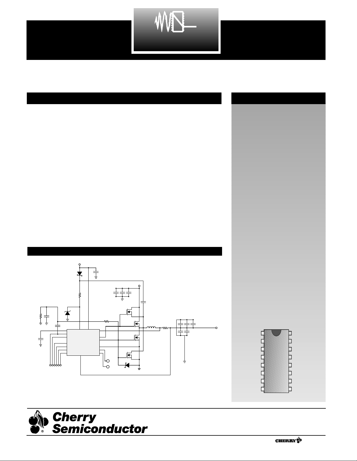
Application Diagram
GATE(H)V
OUT
VID0
VID1
VID2
VID3
VID4
V
FB
V
CC2
PWRGD
OVP
GATE(L)
Gnd
COMP
C
OFF
V
CC1
16 Lead SO Narrow
1
Pentium is a registered trademark of Intel Corporation.
A Company
®
V2is a trademark of Switch Power, Inc.
Rev. 3/11/99
Cherry Semiconductor Corporation
2000 South County Trail, East Greenwich, RI 02818
Tel: (401)885-3600 Fax: (401)885-5786
Email: info@cherry-semi.com
Web Site: www.cherry-semi.com
12V to 16A high performance converter.
The CS51312 is a synchronous dual
NFET Buck Regulator Controller. It is
designed to power the core logic of
the latest high performance CPUs and
ASICs from a single 12V input. It uses
the V
2
TM
control method to achieve
the fastest possible transient response
and best overall regulation. It incorporates many additional features
required to ensure the proper operation and protection of the CPU and
Power system. The CS51312 provides
the industry’s most highly integrated
solution, minimizing external component count, total solution size, and
cost.
The CS51312 is specifically designed
to power Intel’s Pentium
®
II processor
and includes the following features:
5-bit DAC with 1.2% tolerance,
Power-Good output, overcurrent hiccup mode protection, overvoltage
protection, V
CC
monitor, Soft Start,
adaptive voltage positioning, adaptive FET non-overlap time, and
remote sense. The CS51312 will operate over a 9V to 20V (V
CC2
) range
using either single or dual input voltage and is available in 16 lead narrow
body surface mount package.
R2
200
C9
0.01µF
C10
1µF
C19
1000pF
12V
C1
1.0µF
D1
SS16GICT-ND
R1
22Ω
D2
ZM4746ACT-ND
V
ID4
V
ID3
V
ID2
V
ID1
C
OFF
COMP
V
ID0
V
CC2VCC1
V
FB
GATE(H)
GATE(L)
Gnd
OVP
PWRGDV
OUT
CS51312
12V
C2 C3 C4
220µF
16SV220
C6
0.010µF
FY10AAJ-03A
FY10AAJ-03A
Q1
Q2
Q3
FY10AAJ-03A
FY10AAJ-03A
Q4
D3
SS12GICT-ND
OVP
PWRGD
R3
10k
L1
1.2µH
R4
0.004Ω
C14 C15
470µF
C11 C12 C13
470µF
1.25V to 3.5V
T510X477K006AS4394
98
6
10
12
11
13
14
15
16
1
2
3
4
5
7
1
DAC
ENABLE
+++
+++
++
1
1
Page 2
2
Package Pin Description
PACKAGE PIN # PIN SYMBOL FUNCTION
Absolute Maximum Ratings
Pin Symbol Pin Name
V
MAX
V
MIN
I
SOURCE
I
SINK
CS51312
Operating Junction Temperature, TJ . . . . . . . . . . . . . . . . . . . . . . . . . . . . . . . . . . . . . . . . . . . . . . . . . . . . . . . . . . . . . . . 150°C
Lead Temperature Soldering
Reflow (SMD styles only) . . . . . . . . . . . . . . . . . . . . . . . . . . . . . . . . . . . . . . . . . . .60 sec. max above 183°C, 230°C peak
Storage Temperature Range, TS . . . . . . . . . . . . . . . . . . . . . . . . . . . . . . . . . . . . . . . . . . . . . . . . . . . . . . . . . . . . . -65° to 150°C
ESD Susceptibility . . . . . . . . . . . . . . . . . . . . . . . . . . . . . . . . . . . . . . . . . . . . . . . . . . . . . . . . . . . . . . . . . . . . . . . . . . . . . . . . 2kV
V
CC1
IC Bias and Low Side Driver 16V -0.3V N/A 1.5A Peak
Power Input 200mA
V
CC2
IC High Side Driver Power Input 20V -0.3V N/A 1.5A Peak
200mA
COMP Compensation Pin 6V -0.3V 1mA 5mA
V
FB
, V
OUT
, V
ID0-4
Voltage Feedback Input, Output 6V -0.3V 1mA 1mA
Voltage Sense Pin, Voltage
ID DAC Inputs
C
OFF
Off-Time Pin 6V -0.3V 1mA 50mA
GATE(H) High-Side FET Driver 20V -0.3V DC 1.5APeak 1.5A Peak
GATE(L) Low-Side FET Driver 16V 200mA DC 200mA DC
PWRGD Power-Good Output 6V -0.3V 1mA 30mA
OVP Overvoltage Protection 15V -0.3V 30mA 1mA
Gnd Ground 0V 0V 1.5A Peak N/A
200mA DC
1,2,3,4,5 V
IDO
– V
ID4
Voltage ID DAC inputs. These pins are internally pulled up to
5.65V if left open. V
ID4
selects the DAC range. When V
ID4
is
high (logic one), the Error Amp reference range is 2.125V to
3.525V with 100mV increments. When V
ID4
is low (logic zero),
the Error amp reference voltage is 1.325V to 2.075V with 50mV
increments.
6V
FB
Error amp inverting input, PWM comparator non-inverting
input, current limit comparator non-inverting input, PWRGD
and OVP comparator input.
7V
OUT
Current limit comparator inverting input.
8V
CC1
Input power supply pin for the internal circuitry and low side
gate driver. Decouple with filter capacitor to Gnd.
9V
CC2
Input power supply pin for the high side gate driver.
Decouple with filter capacitor to Gnd.
10 GATE(H) High side switch FET driver pin .
11 Gnd Ground pin and IC substrate connection.
12 GATE(L) Low side synchronous FET driver pin.
13 OVP Overvoltage protection pin. Drives high when overvoltage
condition is detected on V
FB
.
14 PWRGD Power-Good Output. Open collector output drives low when
V
FB
is out of regulation.
15 C
OFF
Off-Time Capacitor Pin. A capacitor from this pin to Gnd sets
the off time for the regulator
16 COMP Error amp output. PWM comparator inverting input.
A capacitor on this pin provides error amp compensation, and
determines the Soft Start and hiccup timing. Pulling COMP
below 1.1V (typ) turns off both GATE drivers and shuts down
the regulator.
Page 3
Electrical Characteristics: 0˚C < TA< 70˚C; 0˚C < TJ< 125˚C; 9V < V
CC1
< 14V; 9V ≤ V
CC2
≤ 20V;
2.0V DAC Code(V
ID4
= V
ID3=VID2
= V
ID1
= 0, V
ID0
= 1), C
GATE(H)
= C
GATE(L)
= 3.3nF, C
OFF
= 390pF; Unless otherwise stated.
PARAMETER TEST CONDITIONS MIN TYP MAX UNIT
3
CS51312
■ Voltage Identification DAC
Measure VFB= V
COMP
, VCC= 12V (Note 1)
75°C ≤ TJ≤ 125°C 25°C ≤ TJ≤ 75°C
V
ID4VID3VID2VID1VID0
MIN TYP MAX ± TOL MIN TYP MAX ± TOL UNIT
■ Error Amplifier
V
FB
Bias Current 0.2V ≤VFB≤ 3.5V -7.0 0.1 7.0 µA
COMP Source Current V
COMP
= 1.2V to 3.6V; VFB= 1.9 V 15 30 60 µA
COMP Sink Current V
COMP
=1.2V; VFB= 2.1V; 30 60 120 µA
Open Loop Gain C
COMP
= 0.1µF 80 dB
Unity Gain Bandwidth C
COMP
= 0.1µF 50 kHz
PSRR @ 1kHz C
COMP
= 0.1µF 70 dB
Transconductance 32 mmho
Output Impedance 0.5 MΩ
10000 3.483 3.525 3.567 1.2% 3.455 3.525 3.596 2.0% V
10001 3.384 3.425 3.466 1.2% 3.357 3.425 3.494 2.0% V
10010 3.285 3.325 3.365 1.2% 3.259 3.325 3.392 2.0% V
10011 3.186 3.225 3.264 1.2% 3.161 3.225 3.290 2.0% V
10100 3.087 3.125 3.163 1.2% 3.063 3.125 3.188 2.0% V
10101 2.989 3.025 3.061 1.2% 2.965 3.025 3.086 2.0% V
10110 2.890 2.925 2.960 1.2% 2.875 2.925 2.975 1.7% V
10111 2.791 2.825 2.859 1.2% 2.777 2.825 2.873 1.7% V
11000 2.692 2.725 2.758 1.2% 2.679 2.725 2.771 1.7% V
11001 2.594 2.625 2.657 1.2% 2.580 2.625 2.670 1.7% V
11010 2.495 2.525 2.555 1.2% 2.482 2.525 2.568 1.7% V
11011 2.396 2.425 2.454 1.2% 2.389 2.425 2.461 1.5% V
11100 2.297 2.325 2.353 1.2% 2.290 2.325 2.360 1.5% V
11101 2.198 2.225 2.252 1.2% 2.192 2.225 2.258 1.5% V
11110 2.099 2.125 2.151 1.2% 2.093 2.125 2.157 1.5% V
00000 2.050 2.075 2.100 1.2% 2.044 2.075 2.106 1.5% V
00001 2.001 2.025 2.049 1.2% 1.995 2.025 2.055 1.5% V
00010 1.953 1.975 1.997 1.1% 1.945 1.975 2.005 1.5% V
00011 1.904 1.925 1.946 1.1% 1.896 1.925 1.954 1.5% V
00100 1.854 1.875 1.896 1.1% 1.847 1.875 1.903 1.5% V
00101 1.805 1.825 1.845 1.1% 1.798 1.825 1.852 1.5% V
00110 1.755 1.775 1.795 1.1% 1.748 1.775 1.802 1.5% V
00111 1.706 1.725 1.744 1.1% 1.699 1.725 1.751 1.5% V
01000 1.656 1.675 1.694 1.1% 1.650 1.675 1.700 1.5% V
01001 1.607 1.625 1.643 1.1% 1.601 1.625 1.649 1.5% V
01010 1.558 1.575 1.593 1.1% 1.551 1.575 1.599 1.5% V
01011 1.508 1.525 1.542 1.1% 1.502 1.525 1.548 1.5% V
01100 1.459 1.475 1.491 1.1% 1.453 1.475 1.497 1.5% V
01101 1.409 1.425 1.441 1.1% 1.404 1.425 1.446 1.5% V
01110 1.360 1.375 1.390 1.1% 1.354 1.375 1.396 1.5% V
01111 1.310 1.325 1.340 1.1% 1.305 1.325 1.345 1.5% V
11111 1.225 1.250 1.275 2.0% 1.225 1.250 1.275 2.0% V
Page 4

PARAMETER TEST CONDITIONS MIN TYP MAX UNIT
4
CS51312
Electrical Characteristics: 0˚C < TA< 70˚C; 0˚C < TJ< 125˚C; 9V < V
CC1
< 14V; 9V ≤ V
CC2
≤ 20V;
2.0V DAC Code(V
ID4
= V
ID3=VID2
= V
ID1
= 0, V
ID0
= 1), C
GATE(H)
= C
GATE(L)
= 3.3nF, C
OFF
= 390pF; Unless otherwise stated.
Line Regulation 9V ≤ V
CC1
≤ 14V 0.01 %/V
Input Threshold V
ID4
, V
ID3
, V
ID2
, V
ID1
, V
ID0
1.00 1.25 2.40 V
Input Pull-up Resistance V
ID4
, V
ID3
, V
ID2
, V
ID1
, V
ID0
25 50 100 kΩ
Pull-up Voltage 5.48 5.65 5.82 V
■ GATE(H) and GATE(L)
High Voltage at 100mA Measure V
CC1/2
–GATE(L)/(H) 1.2 2.1 V
Low Voltage at 100mA Measure GATE(L)/(H) 1.0 1.5 V
Rise Time 1.6V < GATE(H)/(L) < (V
CC1/2
– 2.5V) 40 80 ns
Fall Time (V
CC1/2
– 2.5V) > GATE(L)/(H) > 1.6V 40 80 ns
GATE(H) to GATE(L) Delay GATE(H)<2V, GATE(L)>2V, V
CC1/2
= 12V 30 65 110 ns
GATE(L) to GATE(H) Delay GATE(L)<2V, GATE(H)>2V,V
CC1/2
= 12V 30 65 110 ns
GATE pull-down Resistance to Gnd (Note 2) 20 50 115 kΩ
■ Overcurrent Protection
OVC Comparator Offset Voltage 0V ≤ V
OUT
≤ 3.5V 77 86 101 mV
Discharge Threshold Voltage 0.2 0.25 0.3 V
V
OUT
Bias Current 0.2V ≤ V
OUT
≤ 3.5V -7.0 0.1 7.0 µA
OVC Latch Discharge Current V
COMP
= 1V 100 800 2500 µA
■ PWM Comparator
PWM Comparator Offset Voltage 0V ≤ V
FB
≤ 3.5V 0.99 1.10 1.23 V
Transient Response V
FB
= 0 to 3.5V 200 300 ns
■ C
OFF
Off-Time 1.0 1.6 2.3 µs
Charge Current V
COFF
= 1.5V 550 µA
Discharge Current V
COFF
= 1.5V 25 mA
■ Power-Good Output
PWRGD Sink Current V
FB
= 1.7V, V
PWRGD
= 1V 0.5 4 15 mA
PWRGD Upper Threshold % of nominal DAC code 5 8.5 12 %
PWRGD Lower Threshold % of nominal DAC code -12 -8.5 -5 %
PWRGD Output Low Voltage V
FB
= 1.7V, I
PWRGD
= 500µA 0.2 0.3 V
■ Overvoltage Protection (OVP) Output
OVP Source Current OVP = 1V 1 10 25 mA
OVP Threshold % of nominal DAC code 5 8.5 12 %
OVP Pull-up Voltage I
OVP
= 1mA, V
CC1
- V
OVP
1.1 1.5 V
Page 5
CS51312
5
PARAMETER TEST CONDITIONS MIN TYP MAX UNIT
Electrical Characteristics: 0˚C < TA< 70˚C; 0˚C < TJ< 125˚C; 9V < V
CC1
< 14V; 9V ≤ V
CC2
≤ 20V;
2.0V DAC Code(V
ID4
= V
ID3=VID2
= V
ID1
= 0, V
ID0
= 1), C
GATE(H)
= C
GATE(L)
= 3.3nF, C
OFF
= 390pF; Unless otherwise stated.
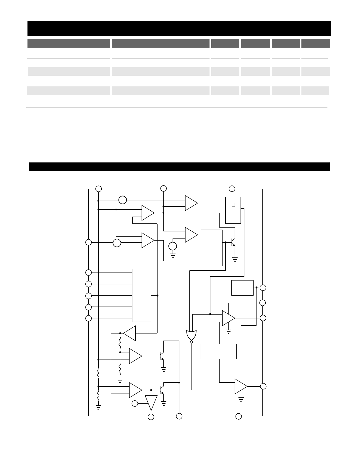
Block Diagram
■ General Electrical Specifications
V
CC1
Monitor Start Threshold 7.9 8.4 8.9 V
V
CC1
Monitor Stop Threshold 7.6 8.1 8.6 V
Hysteresis Start - Stop 0.15 0.30 0.60 V
V
CC1
Supply Current No Load on GATE(H), GATE(L) 9.5 16 mA
V
CC2
Supply Current No Load on GATE(H), GATE(L) 2.5 4.5 mA
Note 1: The IC power dissipation in a typical application with VCC= 12V, switching frequency fSW= 250kHz, 50nc
MOSFETs and R
θJA
= 115°C/W yields an operating junction temperature rise of approximately 52°C, and a junction tem-
perature of 77°C with an ambient temperature of 25°C.
Note 2: Guaranteed by design, not 100% tested in production.
+
-
+
-
+
-
V
FB
COMP
C
OFF
OFF
TIME
PWM COMP
DISCHARGE
COMP
+
-
V
OUT
V
ID0
V
ID1
V
ID2
V
ID3
V
ID4
DAC
+
-
+
-
+
-
1.1V
EA
CURRENT LIMIT
+
-
86mV
0.25V
FAULT
LATCH
R
S
Q
V
CC1
OVP PWRGD Gnd
GATE(L)
GATE(H)
V
CC1
UVLO
NONOVERLAP
LOGIC
+
-
V
CC2
Page 6
CS51312
6
Application Information
V
2
TM
Control Method
The V
2
TM
method of control uses a ramp signal that is generated by the ESR of the output capacitors. This ramp is
proportional to the AC current through the main inductor
and is offset by the value of the DC output voltage. This
control scheme inherently compensates for variation in
either line or load conditions, since the ramp signal is generated from the output voltage itself. This control scheme
differs from traditional techniques such as voltage mode,
which generates an artificial ramp, and current mode,
which generates a ramp from inductor current.
The V
2
TM
control method is illustrated in Figure 6. The output voltage is used to generate both the error signal and
the ramp signal. Since the ramp signal is simply the output
voltage, it is affected by any change in the output regardless of the origin of that change. The ramp signal also con-
tains the DC portion of the output voltage, which allows
the control circuit to drive the main switch to 0% or 100%
duty cycle as required.
Figure 6: V
2
TM
Control Diagram
Theory Of Operation
Typical Performance Characteristics
150
125
100
75
50
25
0
0 2000 4000 6000 8000 10000 12000 14000 16000
Falltime (ns)
Load Capacitance (pF)
VCC = 12V
T
A
= 25°C
Figure 4: Percent Output Error vs. DAC Output
Voltage Setting, V
ID4
= 0.
Figure 1: Gate(H) and Gate(L) Falltime vs. Load Capacitance.
Figure 2: Gate(H) and Gate(L) Risetime vs. Load Capacitance.
Figure 3: DAC Output Voltage vs. Temperature,
DAC Code = 00001.
0.10
0.05
0
−0.05
−0.10
−0.15
−0.20
1.325 1.375 1.425 1.475 1.525 1.575 1.625 1.675 1.725 1.775 1.825 1.875 1.925 1.975 2.025 2.075
DAC Output Voltage Setting (V)
Output Error (%)
VCC = 12V
T
A
= 25°C
V
ID4
= 0
Figure 5: Percent Output Error vs. DAC Output
Voltage Setting, V
ID4
= 1.
0.35
0.30
0.25
0.20
0.15
0.10
0.05
0
−0.05
−0.10
−0.15
−0.20
−0.25
Output Error (%)
2.125 2.225 2.325 2.425 2.525 2.625 2.725 2.825 2.925 3.025 3.125 3.225 3.335 3.425 3.525
DAC Output Voltage Setting (V)
VCC = 12V
T
A
= 25°C
V
ID4
= 1
150
125
100
75
50
25
0
0 2000 4000 6000 8000 10000 12000 14000 16000
Risetime (ns)
Load Capacitance (pF)
VCC = 12V
T
A
= 25°C
0.10
0.05
0
−0.05
−0.10
−0.15
0 20 40 60 80 100 120
Junction Temperature (°C)
DAC Output Voltage
Deviation (%)
VCC = 12V
COMP
PWM
Comparator
–
+
Ramp Signal
Error
Signal
C
Error
Amplifier
GATE(H)
GATE(L)
E
Output
Voltage
Feedback
V
FB
–
+
Reference
Voltage
Page 7

7
Application Information: continued
CS51312
A change in line voltage changes the current ramp in the
inductor, affecting the ramp signal, which causes the V
2
TM
control scheme to compensate the duty cycle. Since the
change in inductor current modifies the ramp signal, as in
current mode control, the V
2
TM
control scheme has the same
advantages in line transient response.
A change in load current will have an affect on the output
voltage, altering the ramp signal. A load step immediately
changes the state of the comparator output, which controls
the main switch. Load transient response is determined
only by the comparator response time and the transition
speed of the main switch. The reaction time to an output
load step has no relation to the crossover frequency of the
error signal loop, as in traditional control methods.
The error signal loop can have a low crossover frequency,
since transient response is handled by the ramp signal loop.
The main purpose of this ‘slow’ feedback loop is to provide
DC accuracy. Noise immunity is significantly improved,
since the error amplifier bandwidth can be rolled off at a
low frequency. Enhanced noise immunity improves remote
sensing of the output voltage, since the noise associated
with long feedback traces can be effectively filtered.
Line and load regulation are drastically improved because
there are two independent voltage loops. A voltage mode
controller relies on a change in the error signal to compensate for a deviation in either line or load voltage. This
change in the error signal causes the output voltage to
change corresponding to the gain of the error amplifier,
which is normally specified as line and load regulation.
A current mode controller maintains fixed error signal
under deviation in the line voltage, since the slope of the
ramp signal changes, but still relies on a change in the error
signal for a deviation in load. The V
2
TM
method of control
maintains a fixed error signal for both line and load variation, since the ramp signal is affected by both line and load.
Constant Off-Time
To minimize transient response, the CS51312 uses a
Constant Off-Time method to control the rate of output
pulses. During normal operation, the Off-Time of the high
side switch is terminated after a fixed period, set by the
C
OFF
capacitor. Every time the VFBpin exceeds the COMP
pin voltage an Off-Time is initiated. To maintain regulation, the V
2
TM
Control Loop varies switch On-Time. The
PWM comparator monitors the output voltage ramp, and
terminates the switch On-Time.
Constant Off-Time provides a number of advantages.
Switch duty Cycle can be adjusted from 0 to 100% on a
pulse-by pulse basis when responding to transient conditions. Both 0% and 100% Duty Cycle operation can be
maintained for extended periods of time in response to
Load or Line transients.
Programmable Output
The CS51312 is designed to provide two methods for programming the output voltage of the power supply. A five
bit on board digital to analog converter (DAC) is used to
program the output voltage within two different ranges.
The first range is 2.125V to 3.525V in 100mV steps, the second is 1.325V to 2.075V in 50mV steps, depending on the
digital input code. If all five bits are left open, the CS51312
enters adjust mode. In adjust mode, the designer can
choose any output voltage by using resistor divider feedback to the VFBpin, as in traditional controllers. The
CS51312 is specifically designed to meet or exceed Intel’s
Pentium®II specifications.
Error Amplifier
The COMP pin is the output of the error amplifier. A
capacitor to Gnd compensates the error amplifier loop.
Additionally, the built in offset on the PWM Comparator
non-inverting input provides the hiccup timing for the
Over-Current Protection, Soft Start function, and regulator
output enable.
V
CC2
Charge Pump
In order to fully turn on the high side NFET, a voltage
greater than the input voltage must be applied to V
CC2
to
bias the GATE(H) driver. Referring to the application diagram on page 1; a simple charge pump circuit can be
implemented for this purpose through capacitor C6, resistor R1, and diodes D1 and D2. The input voltage, less the
drop in D1 is stored in C6 during the off-time period.
When the high-side FET turns on, it drives the inductor
switching node and C6 high causing schottky diode D1 to
reverse bias. The charge stored in C6 is transferred to V
CC2
through R1. Zener diode D2 clamps the V
CC2
voltage to
18V to prevent the V
CC2
from exceeding its 20V Max rating
(see Figure 7).
Figure 7: V
CC2
Charge Pump Operation (1µs/div).
Channel 1 - Charge Pump Switching Node (10V/div)
Channel 2 - V
CC2
(10V/div)
Channel 3 - GATE(H) (10V/div)
Channel 4 - Inductor Switching Node (10V/div)
Startup
The CS51312 provides a controlled startup of regulator output voltage and features Programmable Soft Start implemented through the Error Amp and external Compensation
Capacitor. This feature, combined with overcurrent protection, prevents stress to the regulator power components
and overshoot of the output voltage during startup.
As Power is applied to the regulator, the CS51312
Undervoltage Lockout circuit (UVL) monitors the ICs supply voltage (V
CC1
) which is typically connected to the +12V
input. The UVL circuit prevents the NFET gates from being
activated until V
CC1
exceeds the 8.4V (typ) threshold.
Page 8

CS51312
Application Information: continued
8
Hysteresis of 300mV (typ) is provided for noise immunity.
The Error Amp Capacitor connected to the COMP pin is
charged by a 30µA current source. This capacitor must be
charged to 1.1V (typ) so that it exceeds the PWM comparator’s offset before the V
2
TM
PWM control loop permits
switching to occur.
When V
CC1
has exceeded 8.4V and COMP has charged to
1.1V, the upper Gate driver (GATE(H)) is activated, turning on the upper FET. This causes current to flow through
the output inductor and into the output capacitors and
load according to the following equation:
I = (V
IN
– V
OUT
) ×
GATE(H) and the upper NFET remain on and inductor current ramps up until the initial pulse is terminated by either
the PWM control loop or the overcurrent protection. This
initial surge of in-rush current minimizes startup time, but
avoids overstressing of the regulator’s power components.
The PWM comparator will terminate the initial pulse if the
regulator output exceeds the voltage on the COMP pin
plus the 1.1V PWM comparator offset prior to the drop
across the current sense resistor exceeding the current limit
threshold. In this case, the PWM control loop has achieved
regulation and the initial pulse is then followed by a constant off time as programmed by the C
OFF
capacitor. The
COMP capacitor will continue to slowly charge and the
regulator output voltage will follow it, less the 1.1V PWM
offset, until it achieves the voltage programmed by the
DAC’s VID input. The Error Amp will then source or sink
current to the COMP cap as required to maintain the correct regulator DC output voltage. Since the rate of increase
of the COMP pin voltage is typically set much slower than
the regulator’s slew capability, inrush current, output voltage, and duty cycle all gradually increase from zero. (See
Figures 8 and 9).
Figure 8: Normal Startup (5ms/div).
Channel 1 - Regulator Input Voltage and V
CC1
(10V/div)
Channel 2 – COMP (2V/div)
Channel 4 - Regulator Output Voltage (1V/div)
Figure 9: Normal Startup showing initial pulse followed by Soft Start
(5µs/div).
Channel 1 - V
CC2
(10V/div)
Channel 2 – GATE(H) (10V/div)
Channel 3 - Inductor Switching Node (10V/div)
Channel 4 - Regulator Output Voltage (2V/div)
If the voltage across the Current Sense resistor generates a
voltage difference between the VFBand V
OUT
pins that
exceeds the OVC Comparator Offset Voltage (86mV typical), the Fault latch is set. This causes the COMP pin to be
quickly discharged, turning off GATE(H) and the upper
NFET since the voltage on the COMP pin is now less than
the 1.1V PWM comparator offset. The Fault latch is reset
when the voltage on the COMP decreases below the
Discharge threshold voltage (0.25V typical). The COMP
capacitor will again begin to charge, and when it exceeds
the 1.1V PWM comparator offset, the regulator output will
Soft Start normally (see Figure 10).
Figure 10: Startup with COMP pre-charged to 2V (2ms/div).
Channel 1 - Regulator Output Voltage (1V/div)
Channel 2 - COMP Pin (1V/div)
Channel 3 - VCC(10V/div)
T
L
Page 9

Application Information: continued
9
CS51312
When driving large capacitive loads, the COMP must
charge slowly enough to avoid tripping the CS51312 overcurrent protection. The following equation can be used to
ensure unconditional startup:
<
where
I
CHG
= COMP Source Current (30µA typical);
C
COMP
= COMP Capacitor value (0.1µF typical);
I
LIM
= Current Limit Threshold;
I
LOAD
= Load Current during startup;
C
OUT
= Total Output Capacitance.
Normal Operation
During Normal operation, Switch Off-Time is constant and
set by the C
OFF
capacitor. Switch On-Time is adjusted by
the V
2TM
Control loop to maintain regulation. This results
in changes in regulator switching frequency, duty cycle,
and output ripple in response to changes in load and line.
Output voltage ripple will be determined by inductor ripple current and the ESR of the output capacitors
Transient Response
The CS51312 V
2
TM
Control Loop’s 200ns reaction time provides unprecedented transient response to changes in
input voltage or output current. Pulse-by-pulse adjustment
of duty cycle is provided to quickly ramp the inductor current to the required level. Since the inductor current cannot
be changed instantaneously, regulation is maintained by
the output capacitor(s) during the time required to slew the
inductor current.
Overall load transient response is further improved
through a feature called “Adaptive Voltage Positioning”.
This technique pre-positions the output capacitors voltage
to reduce total output voltage excursions during changes
in load.
Holding tolerance to 1% allows the error amplifiers reference voltage to be targeted +25mV high without compromising DC accuracy. A “Droop Resistor” connects the
Error Amps feedback pin (VFB) to the output capacitors
and load and carries the output current. With no load,
there is no DC drop across this resistor, producing an output voltage tracking the Error amps, including the +25mV
offset. When the full load current is delivered, a 50mV
drop is developed across this resistor. This results in output voltage being offset -25mV low.
The benefit of Adaptive Voltage Positioning is that additional margin is provided for a load transient before reaching the output voltage specification limits. When load current suddenly increases from its minimum level, the output capacitor is pre-positioned +25mV. Conversely, when
load current suddenly decreases from its maximum level,
the output capacitor is pre-positioned -25mV. For best
Transient Response, a combination of a number of high frequency and bulk output capacitors are usually used.
Protection and Monitoring Features
Over-Current Protection
A hiccup mode current limit protection feature is provided,
requiring only the COMP capacitor to implement. The
CS51312 provides overcurrent protection by sensing the
current through a “Droop” resistor, using an internal current sense comparator. The comparator compares the voltage drop through the “Droop” resistor to an internal reference voltage of 86mV (typical).
If the voltage drop across the “Droop” resistor exceeds this
threshold, the current sense comparator allows the fault
latch to be set. This causes the regulator to stop switching.
During this over current condition, the CS51312 stays off
for the time it takes the COMP pin capacitor to discharge
to its lower 0.25V threshold. As soon as the COMP pin
reaches 0.25V, the Fault latch is reset (no overcurrent condition present) and the COMP pin is charged with a 30µA
current source to a voltage 1.1V greater than the VFBvoltage. Only at this point the regulator attempts to restart normally by delivering short gate pulses to both FETS. This
protection scheme minimizes thermal stress to the regulator components, input power supply, and PC board traces,
as the over current condition persists. Upon removal of the
overload, the fault latch is cleared, allowing normal operation to resume.
Overvoltage Protection
Overvoltage protection (OVP) is provided as result of the
normal operation of the V
2
TM
control topology and requires
no additional external components. The control loop
responds to an overvoltage condition within 200ns, causing
the top MOSFET to shut off, disconnecting the regulator
from its input voltage. This results in a “crowbar” action to
clamp the output voltage and prevents damage to the load.
The regulator will remain in this state until the overvoltage
condition ceases or the input voltage is pulled low.
Additionally, a dedicated Overvoltage protection (OVP)
output pin (pin 13) is provided in the CS51312. The OVP
signal will go high (overvoltage condition), if the output
voltage (V
CC(CORE)
) exceeds the regulation voltage by 8.5%
of the voltage set by the particular DAC code. The OVP pin
can source up to 25mA of current that can be used to drive
an SCR to crowbar the power supply.
Power-Good Circuit
The Power-Good pin (pin 14) is an open-collector signal
consistent with TTL DC specifications. It is externally
pulled up, and is pulled low (below 0.3V) when the regulator output voltage typically exceeds ± 8.5% of the nominal
output voltage. Maximum output voltage deviation before
Power-Good is pulled low is ± 12%.
Output Enable
On/off control of the regulator outputs can be implemented by pulling the COMP pins low. It is required to pull the
COMP pins below the 1.1V PWM comparator offset voltage in order to disable switching on the GATE drivers.
I
LIM
− I
LOAD
C
OUT
I
CHG
C
COMP
Page 10

CS51312
Application Information: continued
10
Adaptive FET Non-Overlap
The CS51312 includes circuitry to prevent the simultaneous
conduction of both the high and low side NFETs. This is
necessary to prevent efficiency reducing “shoot-through”
current from flowing from the input voltage to ground
through the two NFETs. Prior to either GATE(H) or
GATE(L) driving high, the other GATE must reach its low
state. Since GATE rise and fall times vary with loading, this
results in a variable delay from the start of turn-off until
the start of turn-on (see Figure 11).
Figure 11: Adaptive FET Non-Overlap (100ns/div).
Channel 1 - GATE(H) (5V/div)
Channel 2 – GATE(L) (5V/div)
Channel 3 - Inductor Switching Node (10V/div)
Step 1: Definition of the design specifications
The output voltage tolerance can be affected by any or all
of the following reasons:
1) buck regulator output voltage setpoint accuracy;
2) output voltage change due to discharging or charging
of the bulk decoupling capacitors during a load current
transient;
3) output voltage change due to the ESR and ESL of the
bulk and high frequency decoupling capacitors, circuit
traces, and vias;
4) output voltage ripple and noise.
Budgeting the tolerance is left up to the designer who must
take into account all of the above effects and provide an
output voltage that will meet the specified tolerance at the
load.
The designer must also ensure that the regulator component temperatures are kept within the manufacturer’s specified ratings at full load and maximum ambient temperature.
Step 2: Selection of the Output Capacitors
These components must be selected and placed carefully to
yield optimal results. Capacitors should be chosen to provide acceptable ripple on the regulator output voltage. Key
specifications for output capacitors are their ESR
(Equivalent Series Resistance), and ESL (Equivalent Series
Inductance). For best transient response, a combination of
low value/high frequency and bulk capacitors placed close
to the load will be required.
In order to determine the number of output capacitors the
maximum voltage transient allowed during load transitions
has to be specified. The output capacitors must hold the
output voltage within these limits since the inductor current
can not change with the required slew rate. The output
capacitors must therefore have a very low ESL and ESR.
The voltage change during the load current transient is:
∆V
OUT
= ∆I
OUT
×
(
+ ESR +
)
,
where
∆I
OUT
/ ∆t = load current slew rate;
∆I
OUT
= load transient;
∆t = load transient duration time;
ESL = Maximum allowable ESL including capacitors,
circuit traces, and vias;
ESR = Maximum allowable ESR including capacitors and
circuit traces;
tTR= output voltage transient response time.
The designer has to independently assign values for the
change in output voltage due to ESR, ESL, and output
capacitor discharging or charging. Empirical data indicates
that most of the output voltage change (droop or spike
depending on the load current transition) results from the
total output capacitor ESR.
The maximum allowable ESR can then be determined
according to the formula
ESR
MAX
=
,
where ∆V
ESR
= change in output voltage due to ESR
(assigned by the designer).
Once the maximum allowable ESR is determined, the num-
ber of output capacitors can be found by using the formula
Number of capacitors =
,
where
ESR
CAP
= maximum ESR per capacitor (specified in manufacturer’s data sheet);
ESR
MAX
= maximum allowable ESR.
The actual output voltage deviation due to ESR can then be
verified and compared to the value assigned by the designer:
∆V
ESR
= ∆I
OUT
× ESR
MAX
Similarly, the maximum allowable ESL is calculated from
the following formula:
ESL
MAX
=
,
∆V
ESL
× ∆t
∆I
ESR
CAP
ESR
MAX
∆V
ESR
∆I
OUT
t
TR
C
OUT
ESL
∆t
CS51312-based V
CC(CORE)
Buck Regulator Design Procedure
Page 11

Application Information: continued
11
CS51312
where
∆I/∆T = load current slew rate (as high as 20A/µs);
∆V
ESL
= change in output voltage due to ESL.
The actual maximum allowable ESL can be determined by
using the equation:
ESL
MAX
=
,
where ESL
CAP
= maximum ESL per capacitor (it is estimated that a 10 × 12mm Aluminum Electrolytic capacitor has
approximately 4nH of package inductance).
The actual output voltage deviation due to the actual maximum ESL can then be verified:
∆V
ESL
=
.
The designer now must determine the change in output
voltage due to output capacitor discharge during the transient:
∆V
CAP
=
,
where
∆t
TR
= the output voltage transient response time
(assigned by the designer);
∆V
CAP
= output voltage deviation due to output capacitor discharge;
∆I = Load step.
The total change in output voltage as a result of a load current transient can be verified by the following formula:
∆V
OUT
= ∆V
ESR
+ ∆V
ESL
+ ∆V
CAP
Step 3: Selection of the Duty Cycle,
Switching Frequency, Switch On-Time (TON)
and Switch Off-Time (T
OFF
)
The duty cycle of a buck converter (including parasitic
losses) is given by the formula:
Duty Cycle = D =
,
where
V
OUT
= buck regulator output voltage;
V
HFET
= high side FET voltage drop due to R
DS(ON)
;
V
L
= output inductor voltage drop due to inductor wire
DC resistance;
V
DROOP
= droop (current sense) resistor voltage drop;
V
IN
= buck regulator input voltage;
V
LFET
= low side FET voltage drop due to R
DS(ON)
.
Step3a: Calculation of Switch On-Time
The switch On-Time (time during which the switching
MOSFET in a synchronous buck topology is conducting) is
determined by:
T
ON
= ,
where FSW= regulator switching frequency selected by the
designer.
Higher operating frequencies allow the use of smaller
inductor and capacitor values. Nevertheless, it is common
to select lower frequency operation because a higher frequency results in lower efficiency due to MOSFET gate
charge losses. Additionally, the use of smaller inductors at
higher frequencies results in higher ripple current, higher
output voltage ripple, and lower efficiency at light load
currents.
Step 3b: Calculation of Switch Off-Time
The switch Off-Time (time during which the switching
MOSFET is not conducting) can be determined by:
T
OFF
= − TON,
The C
OFF
capacitor value has to be selected in order to set
the Off-Time, T
OFF
, above:
C
OFF
= ,
where
3980 is a characteristic factor of the CS51312;
D = Duty Cycle.
Step 4: Selection of the Output Inductor
The inductor should be selected based on its inductance,
current capability, and DC resistance. Increasing the inductor value will decrease output voltage ripple, but degrade
transient response. There are many factors to consider in
selecting the inductor including cost, efficiency, EMI and
ease of manufacture. The inductor must be able to handle
the peak current at the switching frequency without saturating, and the copper resistance in the winding should be
kept as low as possible to minimize resistive power loss.
There are a variety of materials and types of magnetic
cores that could be used for this application. Among them
are ferrites, molypermalloy cores (MPP), amorphous and
powdered iron cores. Powdered iron cores are very commonly used. Powdered iron cores are very suitable due to
their high saturation flux density and have low loss at high
frequencies, a distributed gap and exhibit very low EMI.
The inductor value can be determined by:
L = ,
where
VIN= input voltage;
V
OUT
= output voltage;
t
TR
= output voltage transient response time (assigned
by the designer);
∆I = load transient.
The inductor ripple current can then be determined:
∆I
L
= ,
V
OUT
× T
OFF
L
(VIN− V
OUT
) × t
TR
∆Ι
Period × (1 − D)
3980
1
F
SW
Duty Cycle
F
SW
V
OUT
+ (V
HFET
+ VL+ V
DROOP
)
V
IN
+ V
LFET
− V
HFET
− V
L
∆I × ∆t
TR
C
OUT
ESL
MAX
× ∆I
∆t
ESL
CAP
Number of output capacitors
Page 12

CS51312
12
Application Information: continued
where
∆IL= inductor ripple current;
V
OUT
= output voltage;
T
OFF
= switch Off-Time;
L = inductor value.
The designer can now verify if the number of output
capacitors from step 2 will provide an acceptable output
voltage ripple (1% of output voltage is common). The formula below is used:
∆IL= ,
Rearranging we have:
ESR
MAX
= ,
where
ESR
MAX
= maximum allowable ESR;
∆V
OUT
= 1% × V
OUT
= maximum allowable output voltage ripple ( budgeted by the designer );
∆IL= inductor ripple current;
V
OUT
= output voltage.
The number of output capacitors is determined by:
Number of capacitors =
,
where ESR
CAP
= maximum ESR per capacitor (specified in
manufacturer’s data sheet).
The designer must also verify that the inductor value
yields reasonable inductor peak and valley currents (the
inductor current is a triangular waveform):
I
L(PEAK)
= I
OUT
+
,
where
I
L(PEAK)
= inductor peak current;
I
OUT
= load current;
∆IL= inductor ripple current.
I
L(VALLEY)
= I
OUT
−
,
where I
L(VALLEY)
= inductor valley current.
Step 5: Selection of the Input Capacitors
These components must be selected and placed carefully to
yield optimal results. Capacitors should be chosen to provide acceptable ripple on the input supply lines. A key
specification for input capacitors is their ripple current rating. The input capacitor should also be able to handle the
input RMS current I
IN(RMS)
.
The combination of the input capacitors CINdischarges
during the on-time.
The input capacitor discharge current is given by:
I
CINDIS(RMS)
=
,
where
I
CINDIS(RMS)
= input capacitor discharge current;
I
L(PEAK)
= inductor peak current;
I
L(VALLEY)
= inductor valley current.
CINcharges during the off-time, the average current
through the capacitor over one switching cycle is zero:
I
CIN(CH)
= I
CIN(DIS)
× ,
where
I
CIN(CH)
= input capacitor charge current;
I
CIN(DIS)
= input capacitor discharge current;
D = Duty Cycle.
The total Input RMS current is:
I
CIN(RMS)
= (I
CIN(DIS)
2
× D) + (I
CIN(CH)
2
× (1 − D))
The number of input capacitors required is then determined by:
N
CIN
= ,
where
N
CIN
= number of input capacitors;
I
CIN(RMS)
= total input RMS current;
I
RIPPLE
= input capacitor ripple current rating (specified
in manufacturer’s data sheets).
The total input capacitor ESR needs to be determined in
order to calculate the power dissipation of the input capacitors:
ESR
CIN
= ,
where
ESR
CIN
= total input capacitor ESR;
ESR
CAP
= maximum ESR per capacitor (specified in
manufacturer’s data sheets);
N
CIN
= number of input capacitors.
Once the total ESR of the input capacitors is known, the
input capacitor ripple voltage can be determined using the
formula:
V
CIN(RMS)
= I
CIN(RMS)
× ESR
CIN
,
where
V
CIN(RMS)
= input capacitor RMS voltage;
I
CIN(RMS)
= total input RMS current;
ESR
CIN
= total input capacitor ESR.
The designer must determine the input capacitor power
loss in order to ensure there isn’t excessive power dissipation through these components. The following formula is
used:
P
CIN(RMS)
= I
CIN(RMS)
2
× ESR
CIN
ESR
CAP
N
CIN
I
CIN(RMS)
I
RIPPLE
D
1 − D
(I
L(PEAK)
2
+ (I
L(PEAK)
× I
L(VALLEY)
) + I
L(VALLEY)
2
× D
3
∆I
L
2
∆I
L
2
ESR
CAP
ESR
MAX
∆V
OUT
∆I
L
∆V
OUT
ESR
MAX
Page 13

where
P
CIN(RMS)
= input capacitor RMS power dissipation;
I
CIN(RMS)
= total input RMS current;
ESR
CIN
= total input capacitor ESR.
Step 6: Selection of the Input Inductor
A common requirement is that the buck controller must
not disturb the input voltage. One method of achieving
this is by using an input inductor and a bypass capacitor.
The input inductor isolates the supply from the noise generated in the switching portion of the buck regulator and
also limits the inrush current into the input capacitors
upon power up. The inductor’s limiting effect on the input
current slew rate becomes increasingly beneficial during
load transients. The worst case is when the load changes
from no load to full load (load step), a condition under
which the highest voltage change across the input capacitors is also seen by the input inductor. The inductor successfully blocks the ripple current while placing the transient current requirements on the input bypass capacitor
bank, which has to initially support the sudden load
change.
The minimum inductance value for the input inductor is
therefore:
LIN= ,
where
LIN= input inductor value;
∆V = voltage seen by the input inductor during a full
load swing;
(dI/dt)
MAX
= maximum allowable input current slew
rate.
The designer must select the LC filter pole frequency so
that at least 40dB attenuation is obtained at the regulator
switching frequency. The LC filter is a double-pole network with a slope of −2, a roll-off rate of –40dB/dec, and a
corner frequency:
fC= ,
where
L = input inductor;
C = input capacitor(s).
Step 7: Selection of the Power FET
FET Basics
The use of the MOSFET as a power switch is propelled by
two reasons: 1) Its very high input impedance; and 2) Its very
fast switching times. The electrical characteristics of a MOSFET are considered to be those of a perfect switch. Control
and drive circuitry power is therefore reduced. Because the
input impedance is so high, it is voltage driven. The input
of the MOSFET acts as if it were a small capacitor, which
the driving circuit must charge at turn on. The lower the
drive impedance, the higher the rate of rise of V
GS
, and the
faster the turn- on time. Power dissipation in the switching
MOSFET consists of 1) conduction losses, 2) leakage losses,
3) turn-on switching losses, 4) turn-off switching losses,
and 5) gate-transitions losses. The latter three losses are
proportional to frequency. For the conducting power dissi-
pation rms values of current and resistance are used for
true power calculations. The fast switching speed of the
MOSFET makes it indispensable for high-frequency power
supply applications. Not only are switching power losses
minimized, but also the maximum usable switching frequency is considerably higher. Switching time is independent of temperature. Also, at higher frequencies, the use of
smaller and lighter components (transformer, filter choke,
filter capacitor) reduces overall component cost while
using less space for more efficient packaging at lower
weight.
The MOSFET has purely capacitive input impedance. No
DC current is required. It is important to keep in mind the
drain current of the FET has a negative temperature coefficient. Increase in temperature causes higher on-resistance
and greater leakage current. V
DS(ON)
should be low to min-
imize power dissipation at a given I
D
, and VGSshould be
high to accomplish this. MOSFET switching times are
determined by device capacitance, stray capacitance, and
the impedance of the gate drive circuit. Thus the gate driving circuit must have high momentary peak current sourcing and sinking capability for switching the MOSFET. The
input capacitance, output capacitance and reverse-transfer
capacitance also increase with increased device current rating.
Two considerations complicate the task of estimating
switching times. First, since the magnitude of the input
capacitance, C
ISS
, varies with VDS, the RC time constant
determined by the gate-drive impedance and C
ISS
changes
during the switching cycle. Consequently, computation of
the rise time of the gate voltage by using a specific gatedrive impedance and input capacitance yields only a rough
estimate. The second consideration is the effect of the
“Miller” capacitance, C
RSS
, which is referred to as CDGin
the following discussion. For example, when a device is on,
V
DS(ON)
is fairly small and VGSis about 12V. CDGis
charged to V
DS(ON)
− VGS, which is a negative potential if
the drain is considered the positive electrode. When the
drain is “off”, C
DG
is charged to quite a different potential.
In this case the voltage across C
DG
is a positive value since
the potential from gate-to-source is near zero volts and V
DS
is essentially the drain supply voltage. During turn-on and
turn-off, these large swings in gate-to-drain voltage tax the
current sourcing and sinking capabilities of the gate drive.
In addition to charging and discharging CGS, the gate drive
must also supply the displacement current required by
CDG(I
GATE
= CdgdVdg/dt). Unless the gate-drive
impedance is very low, the VGSwaveform commonly
plateaus during rapid changes in the drain-to-source voltage.
The most important aspect of FET performance is the Static
Drain-To-Source On-Resistance (R
DS(ON)
), which effects
regulator efficiency and FET thermal management requirements. The On-Resistance determines the amount of current a FET can handle without excessive power dissipation
that may cause overheating and potentially catastrophic
failure. As the drain current rises, especially above the continuous rating, the On-Resistance also increases. Its positive temperature coefficient is between +0.6%/C and
+0.85%/C. The higher the On-Resistance the larger the
conduction loss is. Additionally, the FET gate charge
should be low in order to minimize switching losses and
reduce power dissipation.
Both logic level and standard FETs can be used.
1
2π LC
∆V
(dI/dt)
MAX
Application Information: continued
13
CS51312
Page 14

CS51312
Application Information: continued
14
Voltage applied to the FET gates depends on the application circuit used. Both upper and lower gate driver outputs
are specified to drive to within 1.5V of ground when in the
low state and to within 2V of their respective bias supplies
when in the high state. In practice, the FET gates will be
driven rail-to-rail due to overshoot caused by the capacitive load they present to the controller IC.
Step 7a - Selection of the switching (upper) FET
The designer must ensure that the total power dissipation
in the FET switch does not cause the power component’s
junction temperature to exceed 150°C.
The maximum RMS current through the switch can be
determined by the following formula:
I
RMS(H)
=
,
where
I
RMS(H)
= maximum switching MOSFET RMS current;
I
L(PEAK)
= inductor peak current;
I
L(VALLEY)
= inductor valley current;
D = Duty Cycle.
Once the RMS current through the switch is known, the
switching MOSFET conduction losses can be calculated:
P
RMS(H)
= I
RMS(H)
2
× R
DS(ON)
where
P
RMS(H)
= switching MOSFET conduction losses;
I
RMS(H)
= maximum switching MOSFET RMS current;
R
DS(ON)
= FET drain-to-source on-resistance
The upper MOSFET switching losses are caused during
MOSFET switch-on and switch-off and can be determined
by using the following formula:
P
SWH
= P
SWH(ON)
+ P
SWH(OFF)
= ,
where
P
SWH(ON)
= upper MOSFET switch-on losses;
P
SWH(OFF)
= upper MOSFET switch-off losses;
VIN= input voltage;
I
OUT
= load current;
t
RISE
= MOSFET rise time (from FET manufacturer’s
switching characteristics performance curve);
t
FALL
= MOSFET fall time (from FET manufacturer’s
switching characteristics performance curve);
T = 1/FSW= period.
The total power dissipation in the switching MOSFET can
then be calculated as:
P
HFET(TOTAL)
= P
RMSH
+ P
SWH(ON)
+ P
SWH(OFF)
,
where
P
HFET(TOTAL)
= total switching (upper) MOSFET losses;
P
RMSH
= upper MOSFET switch conduction Losses;
P
SWH(ON)
= upper MOSFET switch-on losses;
P
SWH(OFF)
= upper MOSFET switch-off losses.
Once the total power dissipation in the switching FET is
known, the maximum FET switch junction temperature
can be calculated:
TJ= TA+ [P
HFET(TOTAL)
× R
θJA
],
where
TJ= FET junction temperature;
TA= ambient temperature;
P
HFET(TOTAL)
= total switching (upper) FET losses;
R
θJA
= upper FET junction-to-ambient thermal resistance
Step 7b: Selection of the synchronous (lower) FET
The switch conduction losses for the lower FET can be calculated as follows:
P
RMSL
= I
RMS
2
× R
DS(ON)
= [I
OUT
× (1 − D)]2× R
DS(ON)
,
where
P
RMSL
= lower MOSFET conduction losses;
I
OUT
= load current;
D = Duty Cycle;
R
DS(ON)
= lower FET drain-to-source on-resistance.
The synchronous MOSFET has no switching losses, except
for losses in the internal body diode, because it turns on
into near zero voltage conditions. The MOSFET body
diode will conduct during the non-overlap time and the
resulting power dissipation (neglecting reverse recovery
losses) can be calculated as follows:
P
SWL
= VSD× I
LOAD
× non-overlap time × FSW,
where
P
SWL
= lower FET switching losses;
VSD= lower FET source-to-drain voltage;
I
LOAD
= load current
Non-overlap time = GATE(L)-to-GATE(H) or GATE(H)to-GATE(L) delay (from CS51312 data sheet Electrical
Characteristics section);
FSW= switching frequency.
The total power dissipation in the synchronous (lower)
MOSFET can then be calculated as:
P
LFET(TOTAL)
= P
RMSL
+ P
SWL
,
where
P
LFET(TOTAL)
= Synchronous (lower) FET total losses;
P
RMSL
= Switch Conduction Losses;
P
SWL
= Switching losses.
Once the total power dissipation in the synchronous FET is
known the maximum FET switch junction temperature can
be calculated:
TJ= TA+ [P
LFET(TOTAL)
× R
θJA
],
where
TJ= MOSFET junction temperature;
TA= ambient temperature;
P
LFET(TOTAL)
= total synchronous (lower) FET losses;
R
θJA
= lower FET junction-to-ambient thermal resistance.
VIN× I
OUT
× (t
RISE
+ t
FALL
)
6T
(I
L(PEAK)
2
+ (I
L(PEAK)
× I
L(VALLEY)
) + I
L(VALLEY)
2
× D
3
Page 15

Application Information: continued
15
CS51312
Step 8: Control IC Power Dissipation
The power dissipation of the IC varies with the MOSFETs
used, V
CC
, and the CS51312 operating frequency. The average MOSFET gate charge current typically dominates the
control IC power dissipation.
The IC power dissipation is determined by the formula:
P
CONTROLIC
= I
CC1VCC1
+ P
GATE(H)
+ P
GATE(L)
,
where
P
CONTROLIC
= control IC power dissipation;
I
CC1
= IC quiescent supply current;
V
CC1
= IC supply voltage;
P
GATE(H)
= upper MOSFET gate driver (IC) losses;
P
GATE(L)
= lower MOSFET gate driver (IC) losses.
The upper (switching) MOSFET gate driver (IC) losses are:
P
GATE(H)
= Q
GATE(H)
× FSW× V
GATE(H)
,
where
P
GATE(H)
= upper MOSFET gate driver (IC) losses;
Q
GATE(H)
= total upper MOSFET gate charge;
F
SW
= switching frequency;
V
GATE(H)
= upper MOSFET gate voltage.
The lower (synchronous) MOSFET gate driver (IC) losses
are:
P
GATE(L)
= Q
GATE(L)
× FSW× V
GATE(L)
,
where
P
GATE(L)
= lower MOSFET gate driver (IC) losses;
Q
GATE(L)
= total lower MOSFET gate charge;
F
SW
= switching frequency;
V
GATE(L)
= lower MOSFET gate voltage.
The junction temperature of the control IC is primarily a
function of the PCB layout, since most of the heat is
removed through the traces connected to the pins of the IC.
Step 9: Slope Compensation
Voltage regulators for today’s advanced processors are
expected to meet very stringent load transient requirements. One of the key factors in achieving tight dynamic
voltage regulation is low ESR at the CPU input supply
pins. Low ESR at the regulator output results in low output
voltage ripple. The consequence is, however, that there’s
very little voltage ramp at the control IC feedback pin (VFB)
and regulator sensitivity to noise and loop instability are
two undesirable effects that can surface. The performance
of the CS51312-based CPU V
CC(CORE)
regulator is
improved when a fixed amount of slope compensation is
added to the output of the PWM Error Amplifier (COMP
pin) during the regulator Off-Time. Referring to Figure 12,
the amount of voltage ramp at the COMP pin is dependent
on the gate voltage of the lower (synchronous) FET and the
value of resistor divider formed by R1and R2.
V
SLOPECOMP
= V
GATE(L)
×
( )
×(1 − e),
where
V
SLOPECOMP
= amount of slope added;
V
GATE(L)
= lower MOSFET gate voltage;
R1, R2 = voltage divider resistors;
t = tONor t
OFF
(switch off-time);
τ = RC constant determined by C1 and the parallel combination of R1, R2 (Figure 12), neglecting the low driver
output impedance.
Figure 12: Small RC filter provides the proper voltage ramp at the beginning of each on-time cycle.
The artificial voltage ramp created by the slope compensation scheme results in improved control loop stability provided that the RC filter time constant is smaller than the
off-time cycle duration (time during which the lower MOSFET is conducting). It is important that the series combination of R1 and R2 is high enough in resistance to avoid
loading the GATE(L) pin.
Step 10: Selection of Current Limit Filter Components
In some applications, the current limit comparator may
falsely trigger due to noise, load transients, or high inductor ripple currents. A filter circuit such as the one shown in
Figure 13 can be added to prevent this. The RC time constant of this filter is equal to (R
FB
+ R
OUT
) × C
SENSE
.
Increasing the RC time constant will reduce the sensitivity
of the circuit, but increase the time required to detect an
overcurrent condition. The value of RFB+ R
OUT
should be
kept to 510Ω or lower to avoid significant DC offsets due
to the VFBand V
OUT
bias currents.
Figure 13: Current limit filter circuit.
Adaptive voltage positioning is used to help keep the output voltage within specification during load transients. To
implement adaptive voltage positioning a “Droop
Resistor” must be connected between the output inductor
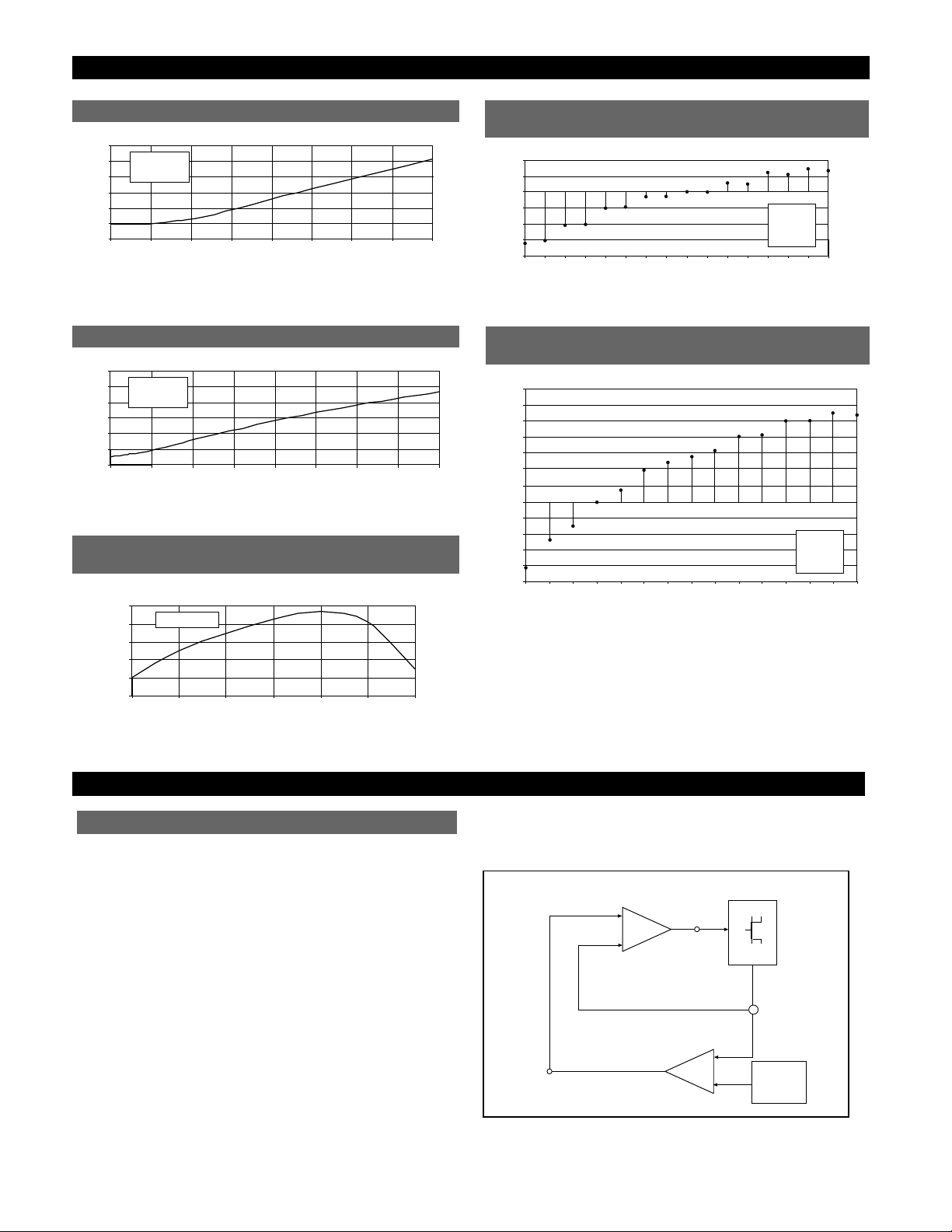
“Droop” Resistor for Adaptive Voltage Positioning
and Current Limit
-t
τ
R2
R1 + R2
COMP
12
16
R
C
COMP
2
C
R
1
1
To Synchronous FET
CS51312
GATE(L)
FB
V
IN
R
FB
RSENSE
R
C
SENSE
OUT
GATE(H)
GATE(L)
V
V
OUT
+
V
OUT
Page 16

CS51312
Application Information: continued
16
and output capacitors and load. This resistor carries the
full load current and should be chosen so that both DC and
AC tolerance limits are met.
In order to determine the droop resistor value the nominal
voltage drop across it at full load has to be calculated. This
voltage drop has to be such that the output voltage at full
load is above the minimum DC tolerance spec:
V
DROOP(TYP)
= .
Current Limit
The current limit setpoint has to be higher than the normal
full load current. Attention has to be paid to the current
rating of the external power components as these are the
first to fail during an overload condition. The MOSFET
continuous and pulsed drain current rating at a given case
temperature has to be accounted for when setting the current limit trip point.
Nominal Current Limit Setpoint
From the overcurrent detection data in the electrical characteristics table:
V
TH(TYP)
= 86mV,
I
CL(NOM)
=
Design Rules for Using a Droop Resistor
The basic equation for laying an embedded resistor is:
R
AR
= ρ × or R = ρ × ,
where
A= W × t = cross-sectional area;
ρ= the copper resistivity (µΩ-mil);
L= length (mils);
W = width (mils);
t = thickness (mils).
An embedded PC trace resistor has the distinct advantage
of near zero cost implementation. However, this droop
resistor can vary due to three reasons: 1) the sheet resistivity variation caused by variation in the thickness of the PCB
layer; 2) the mismatch of L/W; and 3) temperature variation.
1) Sheet Resistivity
For one ounce copper, the thickness variation is typically
1.26 mil to 1.48 mil. Therefore the error due to sheet resistivity is:
= ±8%.
2) Mismatch due to L/W
The variation in L/W is governed by variations due to the
PCB manufacturing process. The error due to L/W mismatch is typically 1%.
3) Thermal Considerations
Due to I
2
× R power losses the surface temperature of the
droop resistor will increase causing the resistance to
increase. Also, the ambient temperature variation will contribute to the increase of the resistance, according to the
formula:
R = R20[1+ α20(Τ−20)],
where
R20= resistance at 20˚C;
α =;
T= operating temperature;
R = desired droop resistor value.
For temperature T = 50˚C, the % R change = 12%.
Droop Resistor Tolerance
Tolerance due to sheet resistivity variation ±8%
Tolerance due to L/W error 1%
Tolerance due to temperature variation 12%
Total tolerance for droop resistor 21%
Droop Resistor Length, Width, and Thickness
The minimum width and thickness of the droop resistor
should primarily be determined on the basis of the currentcarrying capacity required, and the maximum permissible
droop resistor temperature rise. PCB manufacturer design
charts can be used in determining current- carrying capacity and sizes of etched copper conductors for various temperature rises above ambient.
Thermal Management
Thermal Considerations for Power MOSFET
In order to maintain good reliability, the junction temperature of the semiconductor components should be kept to a
maximum of 150°C or lower. The thermal impedance
(junction to ambient) required to meet this requirement
can be calculated as follows:
Thermal Impedance =
A heatsink may be added to TO-220 components to reduce
their thermal impedance. A number of PC board layout
techniques such as thermal vias and additional copper foil
area can be used to improve the power handling capability
of surface mount components.
EMI Management
As a consequence of large currents being turned on and off
at high frequency, switching regulators generate noise as a
consequence of their normal operation. When designing
for compliance with EMI/EMC regulations, additional
components may be added to reduce noise emissions.
These components are not required for regulator operation
and experimental results may allow them to be eliminated.
The input filter inductor may not be required because bulk
T
J(MAX)
- T
A
Power
0.00393
˚C
1.48 - 1.26
1.37
L
(W × t)
L
A
V
TH(TYP)
R
SENSE(NOM)
V
DAC(MIN)-VDC(MIN)
1+R
DROOP(TOLERANCE)
Page 17

Application Information: continued
17
CS51312
Additional Application Circuit
5V/12V to 2V/19A Converter
filter and bypass capacitors, as well as other loads located
on the board will tend to reduce regulator di/dt effects on
the circuit board and input power supply. Placement of the
power component to minimize routing distance will also
help to reduce emissions.
Layout Guidelines
When laying out the CPU buck regulator on a printed circuit board, the following checklist should be used to
ensure proper operation of the CS51312.
1) Rapid changes in voltage across parasitic capacitors and
abrupt changes in current in parasitic inductors are major
concerns for a good layout.
2) Keep high currents out of sensitive ground connections.
3) Avoid ground loops as they pick up noise. Use star or
single point grounding.
4) For high power buck regulators on double-sided PCBs a
single ground plane (usually the bottom) is recommended.
5) Even though double sided PCBs are usually sufficient
for a good layout, four-layer PCBs are the optimum
approach to reducing susceptibility to noise. Use the two
internal layers as the power and Gnd planes, the top layer
for power connections and components vias, and the bottom layers for the noise sensitive traces.
6) Keep the inductor switching node small by placing the
output inductor, switching and synchronous FETs close
together.
7) The MOSFET gate traces to the IC must be as short,
straight, and wide as possible.
8) Use fewer, but larger output capacitors, keep the capacitors clustered, and use multiple layer traces with heavy
copper to keep the parasitic resistance low.
9) Place the switching MOSFET as close to the +5V input
capacitors as possible.
10) Place the output capacitors as close to the load as possible.
11) Place the VFB,V
OUT
filter resistors (510Ω) in series with
the VFBand V
OUT
pins as close as possible to the pins.
12) Place the C
OFF
and COMP capacitors as close as possi-
ble to the C
OFF
and COMP pins.
13) Place the current limit filter capacitor between the V
FB
and V
OUT
pins, as close as possible to the pins.
14) Connect the filter components of the following pins:
VFB, V
OUT
, C
OFF
, and COMP to the Gnd pin with a single
trace, and connect this local Gnd trace to the output capacitor Gnd.
15) The “Droop” Resistor (embedded PCB trace) has to be
wide enough to carry the full load current.
16) Place the VCCbypass capacitors as close as possible to
the IC.
680pF
GATE(H)
GATE(L)
V
FB
V
OUT
10K
1200µF/10V
x3
3.3mΩ
1.2µH
FS70VSJ-03
FS70VSJ-03
510Ω
0.1µF
510Ω
1200µF/10V
x5
V
CC(CORE)
2.0V@19A
+5V
+12V
VID0
VID1
VID2
VID3
VID4
OVP
1µF
PWRGD
C
OFF
Gnd
V
CC1
COMP
V
CC2
OVP
PWRGD
0.01
µF
0.1
µF
100Ω
Page 18

Ordering Information
Part Number Description
CS51312GD16 16L SO Narrow
CS51312GDR16 16L SO Narrow (tape & reel)
CS51312
© 1999 Cherry Semiconductor Corporation
Rev. 3/11/99
18
Thermal Data 16L
SO Narrow
R
ΘJC
typ 28 ˚C/W
R
ΘJA
typ 115 ˚C/W
D
Lead Count Metric English
Max Min Max Min
16L SO Narrow 10.00 9.80 .394 .386
Package Specification
PACKAGE DIMENSIONS IN mm (INCHES)
PACKAGE THERMAL DATA
Cherry Semiconductor Corporation reserves the right to
make changes to the specifications without notice. Please
contact Cherry Semiconductor Corporation for the latest
available information.
Surface Mount Narrow Body (D); 150 mil wide
1.27 (.050) BSC
0.51 (.020)
0.33 (.013)
6.20 (.244)
5.80 (.228)
4.00 (.157)
3.80 (.150)
1.57 (.062)
1.37 (.054)
D
0.25 (0.10)
0.10 (.004)
1.75 (.069) MAX
1.27 (.050)
0.40 (.016)
REF: JEDEC MS-012
0.25 (.010)
0.19 (.008)
 Loading...