

Page 1
V
CC
BIAS
UVLO
SS
Gnd
GATE
IS
V
FB
R8
0.39Ω
Q2
IRFR220
R5
17.4k
C2
1.5µF,
100V
C1
0.1µF,
100V
R2
200k
10µH
36-75V
IN
L1
R1
510k
Q1
ZVN3310A
T1
D1
MBRD360CT
R3
47Ω
R6
1k
C3
.022µF
C6
.01µF
R7
30.1k
C5
47µF,
10V
ISOLATED
RTN
5V
OUT
ENABLE
48VRTN
D4
R4
10Ω
BAS16LT1
C4
0.47µF,
25V
C8
1000pF
C7
0.1µF
TPS5908
U2
R9
10.0k
C9
1000pF
CS5124
CTX15-14514
Features
■ Line UVLO Monitoring
■ Low Current Sense
Voltage for Resistive
Current Sensing
■ External Synchronization
to Higher or Lower
Frequency Oscillator
(CS5126 Only)
■ Bias for Start up Circuitry
(CS5124 Only)
■ Thermal Shutdown
■ Sleep On/Off Pin
■ Soft Start Timer
■ Leading Edge Blanking
■ Direct Optocoupler
Interface
■ 90ns Propagation Delay
■ 35ns Driver Rise and Fall
Times
■ Sleep Mode
Package Options
CS5124/6
High Performance, Integrated Current Mode
PWM Controllers
CS5124/6
Description
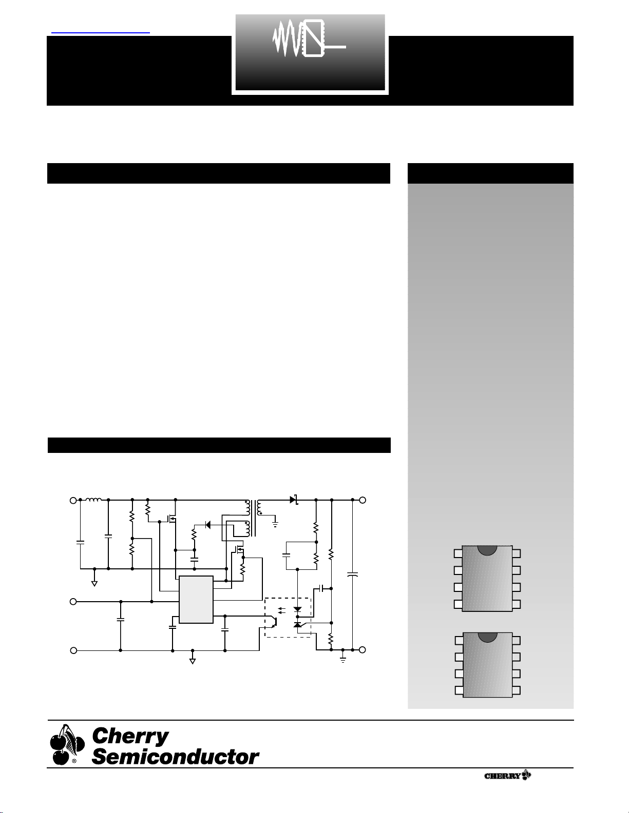
Applications Diagram
8 Lead SO Narrow
1
V
CC
BIAS
UVLO
SS
Gnd
GATE
I
SENSE
V
FB
Cherry Semiconductor Corporation
2000 South County Trail, East Greenwich, RI 02818
Tel: (401)885-3600 Fax: (401)885-5786
Email: info@cherry-semi.com
Web Site: www.cherry-semi.com
A Company
®
Rev. 3/12/99
Gnd
UVLO
V
CC
SYNC
SS
GATE
I
SENSE
V
FB
CS5124
CS5126
48V to 5V, 1A flyback converter using the CS5124
The CS5124/6 is a fixed frequency
current mode controller designed
specifically for DC-DC converters
found in the telecommunications
industry. The CS5124/6 integrates
many commonly required current
mode power supply features and
allows the power supply designer to
realize substantial cost and board
space savings. The product matrix is
as follows:
CS5124: 400kHz w/V
BIAS
Pin,
195mV first current sense threshold
CS5126: 200kHz w/SYNC Pin,
335mV first current sense threshold
The CS5124/6 integrates the following features: Internal Oscillator, Slope
Compensation, Sleep On/Off, Under
Voltage Lock Out, Thermal
Shutdown, Soft Start Timer, Low
Voltage Current Sense for Resistive
Sensing, Second Current Threshold
for Pulse by Pulse Over Current
Protection, a Direct Optocoupler
Interface and Leading Edge Current
Blanking.
The CS5124/6 has supply range of
7.7V to 20V and is available in 8 pin
SO narrow package.
查询CS5124供应商
1
1
Page 2
Pin Symbol Lead Name
V
MAX
V
MIN
I
SOURCE
I
SINK
V
CC
VCCPower Input 20V -0.3V 1mA 1.5A Peak
200mA DC
SYNC (CS5126) Clock Synchronization Input 20V -0.3V 1mA 1mA
V
BIAS
(CS5124) VCCClamp Output 20V -0.3V 1mA 1mA
UVLO UVLO Shutdown Input 6V -0.3V 1mA 1mA
SS Soft Start Capacitor Input 6V -0.3V 1mA 2mA
V
FB
Voltage Feed Back Input 6V -0.3V 3mA 20mA
I
SENSE
Current Sense Input 6V -0.3V 1mA 1mA
GROUND Ground 0V 0V 1.5A peak 1mA
200mA DC
GATE Gate Drive Output 20V -0.3V 1.5A Peak 1.5A Peak
200mA DC 200mA DC
Operating Junction Temperature, T
J
. . . . . . . . . . . . . . . . . . . . . . . . . . . . . . . . . . . . . . . . . . . . . . . . . . . . . . . . . . . . . . .-40 to 135°C
Storage Temperature Range, TS . . . . . . . . . . . . . . . . . . . . . . . . . . . . . . . . . . . . . . . . . . . . . . . . . . . . . . . . . . . . . . . . . . .-40 to 150°C
ESD (Human Body Model) . . . . . . . . . . . . . . . . . . . . . . . . . . . . . . . . . . . . . . . . . . . . . . . . . . . . . . . . . . . . . . . . . . . . . . . . . . . . . .2kV
ESD (Machine Model) . . . . . . . . . . . . . . . . . . . . . . . . . . . . . . . . . . . . . . . . . . . . . . . . . . . . . . . . . . . . . . . . . . . . . . . . . . . . . . . . .200V
Lead Temperature Soldering:
Reflow (SMD styles only) . . . . . . . . . . . . . . . . . . . . . . . . . . . . . . . . . . . . . . . . . . . . . . . . . .60 sec. max above 183°C, 230°C peak
CS5124/6
2
Absolute Maximum Ratings
PARAMETER TEST CONDITIONS MIN TYP MAX UNIT
Electrical Characteristics: -40°C ≤ TJ ≤ 125°C, -40°C ≤ TA ≤ 105°C, 7.60V ≤ V
CC
≤ 20V, UVLO = 3.0V, I
SENSE
= 0V,
C
V(CC)
= 0.33µF, C
GATE
= 1nF (ESR = 10Ω), CSS= 470pF C
V(FB)
= 100pF, unless otherwise stated.
■ General
ICCOperating - V
GATE
not switching. 10 13 mA
ICCat VCCLow VCC= 6V 500 750 µA
ICCSleep V
UVL
= 1V 210 275 µA
■ Low V
CC
Lockout
VCCTurn-on Threshold Voltage 7.2 7.7 8.3 V
VCCTurn-off Threshold Voltage 6.8 7.3 7.8 V
VCCHysteresis 350 425 500 mV
■ UVLO
Sleep Threshold Voltage UVLO decreasing 1.5 1.8 2.3 V
Sleep Threshold Voltage UVLO increasing 1.88 2.45 V
Sleep Hysteresis 35 85 150 mV
UVLO Turn-off (Note 1) 2.3 2.45 2.6 V
Threshold Voltage
UVLO Turn-on (Note 1) 2.50 2.63 2.76 V
Threshold Voltage
UVLO Hysteresis Turn-on – Turnoff (-40°C ≤ TJ≤ 100°C) 170 185 200 mV
(Note 1)
UVLO Hysteresis Turn-on – Turnoff (100°C ≤ TJ≤ 125°C) 50 185 400 mV
(Note 1)
UVLO Input Bias Current -1 1 µA
UVLO Clamp With UVLO sinking 1mA. 5 7.5 12 V
Page 3
CS5124/6
3
Electrical Characteristics: -40°C ≤ TJ ≤ 125°C, -40°C ≤ TA ≤ 105°C, 7.60V ≤ V
CC
≤ 20V, UVLO = 3.0V, I
SENSE
= 0V,
C
V(CC)
= 0.33µF, C
GATE
= 1nF (ESR = 10Ω), CSS= 470pF C
V(FB)
= 100pF, unless otherwise stated.
PARAMETER TEST CONDITIONS MIN TYP MAX UNIT
■ V
CC
Clamp and BIAS Pin CS5124 Only. Connect an NFET as follows: BIAS = G, VCC= S, V
IN
= D.
VCCClamp Voltage 36V ≤ VIN≤ 60V, 220nF ≤ 7.275 7.9 8.625 V
CSS≤ 500nF, R = 500k
BIAS Minimum Voltage Measure Voltage on BIAS with: 1.6 2.8 4 V
10V ≤ VCC≤ 20V and 50µA ≤ I
BIAS
≤ 1mA
BIAS Clamp With BIAS pin sinking 1mA 12 15 20 V
■ 200kHz Oscillator CS5126 Only
Operating Frequency 175 200 225 kHz
Max Duty Cycle Clamp 78 82.5 85 %
Slope Compensation 12 18 23 mV/µs
(Normal operation)
Slope Compensation
(Synchronized operation) (Note 1) 7 12 16 mV/µs
SYNC Input Threshold Voltage 1 2 3 V
SYNC Input Impedance Measured with SYNC = 1V &10V 50 120 230 kΩ
■ 400kHz Oscillator CS5124 Only
Operating Frequency 360 400 440 kHz
Max Duty Cycle Clamp 80.0 82.5 85.0 %
Slope Compensation 15 21 26 mV/µs
■ Soft Start
Soft Start Charge Current 7 10 13 µA
Soft Start Discharge Current 0.5 10.0 mA
VSSVoltage when V
FB
V
FB
= 300mV 1.40 1.62 1.80 V
Begins to Rise
Peak Soft Start Charge Voltage 4.7 4.9 V
Valley Soft Start Discharge Voltage 200 275 400 mV
■ Current Sense CS5124 Only
First Current Sense Threshold At max duty cycle. 170 195 215 mV
Second Current Sense Threshold 250 275 315 mV
I
SENSE
to GATE Prop. Delay 0 to 700mV pulse into I
SENSE
60 90 130 ns
(after blanking time)
Leading Edge Blanking Time 0 to 400mV pulse into I
SENSE
90 130 180 ns
Internal Offset (Note 1) 60 mV
■ Current Sense CS5126 Only
First Current Sense Threshold At max duty cycle 300 335 360 mV
Second Current Sense 485 525 575 mV
Threshold
I
SENSE
to GATE Prop. Delay 0 to 800mV pulse into I
SENSE
60 90 130 ns
(after blanking time)
Leading Edge Blanking Time 0 to 550mV pulse into I
SENSE
110 175 210 ns
Internal Offset (Note 1) 125 mV
Page 4

Package Lead Description
PACKAGE LEAD # LEAD SYMBOL FUNCTION
CS5124/6
4
Electrical Characteristics: -40°C ≤ TJ ≤ 125°C, -40°C ≤ TA ≤ 105°C, 7.60V ≤ V
CC
≤ 20V, UVLO = 3.0V, I
SENSE
= 0V,
C
V(CC)
= 0.33µF, C
GATE
= 1nF (ESR = 10Ω), CSS= 470pF C
V(FB)
= 100pF, unless otherwise stated.
PARAMETER TEST CONDITIONS MIN TYP MAX UNIT
8 Lead SO Narrow
CS5124 CS5126
11 VCCVCCPower Input Pin.
2 - BIAS VCCClamp Output Pin. This pin will control the gate of an N-channel MOS-
FET that in turn regulates VCC. This pin is internally clamped at 15V when
the IC is in sleep mode.
- 3 SYNC Clock Synchronization Pin. A positive edge will terminate the current PWM
cycle. Ground this pin when it is not used.
3 2 UVLO Sleep and under voltage lockout pin. A voltage greater than 1.8V causes the
chip to "wake up" however the GATE remains low. A voltage greater than
2.6V on this pin allows the output to switch.
4 4 SS Soft Start Capacitor Pin. A capacitor placed between SS and GROUND is
charged with 10µA and discharged with 10mA. The Soft Start capacitor controls both soft-start time and hiccup mode frequency.
55 VFBVoltage Feedback Pin. The collector of an optocoupler is typically tied to this
pin. This pin is pulled up internally by a 4.3kΩ resistor to 5V and is clamped
internally at 2.9V(2.65V). If VFBis pulled > 4V, the oscillator is disabled and
GATE will stay high. If the VFBpin is pulled < 0.49V, GATE will stay low.
66I
SENSE
Current Sense Pin. This pin is connected to the current sense resistor on the
primary side. If VFBis floating, the GATE will go low if I
SENSE
= 195mV
(335mV). If I
SENSE
> 275mV (525mV), Soft Start will be initiated.
7 7 GATE Gate Drive Output Pin. Capable of driving a 3nF load. GATE is nominally
clamped to 13.5V.
8 8 Gnd Ground Pin.
■ Voltage Feedback
V
FB
Pull-up Res. 2.9 4.3 8.1 kΩ
VFBClamp Voltage CS5124 Only 2.63 2.90 3.15 V
VFBClamp Voltage CS5126 Only 2.40 2.65 2.90 V
VFBFault Voltage Threshold 460 490 520 mV
■ Output Gate Drive
Maximum Sleep VCC= 6.0V, I
OUT
= 1mA 1.2 2.0 V
Pull-down Voltage
GATE High (AC) Series resistance < 1Ω (Note 1) VCC-1 VCC-0.5 V
GATE Low (AC) Series resistance < 1Ω (Note 1) 0.0 0.5 V
GATE High Clamp Voltage VCC= 20V 11.0 13.5 16.0 V
Rise Time Measure GATE rise time, 45 65 ns
1V < GATE < 9V; V
CC
=12V
Fall Time Measure GATE fall time, 25 55 ns
9V > GATE > 1V; V
CC
= 12V
■ Thermal Shutdown
Thermal Shutdown Temperature (Note 1) (GATE low) 135 150 165 °C
Thermal Enable Temperature (Note 1) (GATE switching) 100 125 150 °C
Thermal Hysteresis (Note 1) 15 25 35 °C
Notes
1. Not tested in production. Specification is guaranteed by design.
Page 5

CS5124/6
5
Block Diagram
V
Theory of Operation
Powering the IC
V
CC
can be powered directly from a regulated supply
and requires 500µA of start-up current. The CS5124/6
includes a line bias pin (BIAS) that can be used to control a
series pass transistor for operation over a wide input voltage. The BIAS pin will control the gate voltage of an Nchannel MOSFET placed between V
IN
and VCCto regulate
V
CC
at 8V.
VCCand UVLO Pins
The UVLO pin has three different modes; low power shutdown, Line UVLO, and normal operation. To illustrate
how the UVLO pin works; assume that VIN, as shown in
the application schematic, is ramped up starting at 0V with
the UVLO pin open. The SS and I
SENSE
pins also start at 0V.
While the UVLO is below 1.8V, the IC will remain in a low
current sleep mode and the BIAS pin of the CS5124 is internally clamped to a maximum of 15V. When the voltage on
the UVLO pin rises to between 1.8V and 2.6V the reference
for the VCCUVLO is enabled and VCCis regulated to 8V by
the BIAS pin (CS5124 only), but the IC remains in a UVLO
state and the output driver does not switch. When the
UVLO pin exceeds 2.6V and the VCCpin exceeds 7.7V, the
GATE pin is released from a low state and can begin
switching based on the comparison of the I
SENSE
and V
FB
pins. The Soft Start capacitor begins charging from 0V at
10µA. As the capacitor charges, a buffered version of the
capacitor voltage appears on the V
FB
pin and the VFBvoltage begins to rise. As VFBrises the duty cycle increases
until the supply comes into regulation.
Soft Start
Soft Start is accomplished by clamping the V
FB
pin 1.32V
below the SS pin during normal start up and during restart
after a fault condition. When the CS5124/6 starts, the Soft
Start capacitor is charged from a 10µA source from 0V to
4.9V. The VFBpin follows the Soft Start pin offset by –1.32V
until the supply comes into regulation or until the Soft
Start error amp is clamped at 2.9V (2.65V for the CS5126).
During fault conditions the Soft Start capacitor is discharged at 10mA.
Fault Conditions
The CS5124/6 recognizes the following faults: UVLO off,
Thermal Shutdown, V
REF(OK)
, and Second Current
Threshold. Once a fault is recognized, fault latch F2 is set
and the IC immediately shuts down the output driver and
discharges the Soft Start capacitor. Soft Start will begin
only after all faults have been removed and the Soft Start
capacitor has been discharged to less than 0.275V. Each
fault will be explained in the following sections.
CC
UVLO
BIAS
(CS5124 ONLY)
SS
UVLO COMP
V
CC
+
-
+
V
7.7 V/7.275V
TSHUT
150°C/125°C
+
LINE AMP
LINE UVLO COMP
+
2.62 V/2.45V
V
V
1.91 V/1.83V
-
+
2.0V
+
REMOTE
(SLEEP) COMP
+
-
V
CC
2.9 R
R
+
V
G2
ENABLE
-
V
REFOK
+
+
V
SOFT START LATCH
F2
G5
S
R
SET DOMAIN
SS COMP
275mV
{CS5126 ONLY}
SYNC
V
CC
V
= 5V
REF
V5
REF
10µA
Q
+
+
V
V5
REF
{2.65V}
2.90V
+
OSC
RAMP
2ND I
+
1.32V
V
DIS
V
G3
COMP
V
FB
PWM COMP
+
{525mV}
-
275mV
+
COMP
V
V5
R
F1
S
RESET DOMAIN
+
+
V
+
+
V
{125mV}
60mV
BLANK
G6
REF
Q
490mV
G1
{85 mV/us}
170mV us
{1/5}
1/10
÷
1000Ω
BLANKING
S
R
F3
G7
+
-
Q
SS AMP
DRIVER
V5
REF
4500Ω
GATE
V
FB
I
SENSE
Gnd
Page 6

CS5124/6
6
Theory of Operation: continued
Application Information
Under Voltage Lockout (UVLO)
The UVLO pin is tied to typically the midpoint of a resistive divider between V
IN
and GROUND. During a start up
sequence, this pin must be above 2.6V in order for the IC to
begin normal operation. If the IC is running and this pin is
pulled below 1.8V, F2 shuts down the output driver and
discharges the Soft Start capacitor in order to insure proper
start-up. If the UVLO pin is pulled high again before the
Soft Start capacitor discharges, the IC will complete the
Soft Start discharge and, if no other faults are present, will
immediately restart the power supply. If the UVLO pin
stays low, then it will enter either the low current sleep
mode or the UVLO state depending on the level of the
UVLO pin.
Thermal Shutdown
If the IC junction temperature exceeds approximately
150°C the thermal shutdown circuit sets F2, which shuts
down the output driver and discharges the Soft Start
capacitor. If no other faults are present the IC will initiate
Soft Start when the IC junction temperature has been
reduced by 25°C.
V
REF(OK)
V
REF(OK)
is an internal monitor that insures the internal
regulator is running before any switching occurs. This
function does not trip the fault comparator like the other
fault functions. To insure that Soft Start will occur at low
line conditions the UVLO divider should be set up so that
the VCCUVLO comparator turns on before the LINE
UVLO comparator.
Second Threshold Comparator
Since the maximum dynamic range of the I
SENSE
signal in
normal operation is 195mV (335mV for the CS5126), any
voltage exceeding this threshold on the I
SENSE
pin is considered a fault and the PWM cycle is terminated. The 2nd
I
COMP
compares the I
SENSE
signal with a 275mV (525mV
for the CS5126) threshold. If the I
SENSE
voltage exceeds the
second threshold, F2 is set, the driver turns off, and the
soft-start capacitor discharges. After the Soft Start capacitor
has discharged to less than 0.275V Soft Start will begin. If
the fault condition has been removed the supply will operate normally. If the fault remains the supply will operate in
hiccup mode until the fault condition is removed.
VFBComparator
The VFBcomparator detects when the output voltage is too
high. When the regulated output voltage is too high, the
feedback loop will drive VFBlow. If VFBis less than 0.49V
the output of the VFBcomparator will go high and shut the
output driver off.
Oscillator
The internally trimmed, 400kHz (CS5124) or 200kHz
(CS5126) provides the slope compensation ramp as well as
the pulse for enabling the output driver.
PWM Comparator and Slope Compensation
The CS5124/6 provides a fixed internal slope compensation ramp that is subtracted from the feedback signal. The
pwm comparator compares peak primary current to a portion of the difference of the feedback voltage and slope
compensation ramp. The 170mV/µs (85mV/µs for the
CS5126) slope compensation ramp is subtracted from the
voltage feedback signal internally. The difference signal is
then divided by ten (five for the CS5126) before the PWM
comparator to provide high noise rejection with a low voltage across the current sense network. (The effective ramp
is 21mV/µs for the CS5124, and 18mV/µs for the CS5126).
A 60mV (125mV for the CS5126) nominal offset on the positive input to the PWM comparator allows for operation
with the I
SENSE
pin at, or even slightly below Gnd.
A 4.3kΩ pull-up resistor internally connected to a 5V nomi-
nal reference provides the bias current to for an opto-coupler connection to the VFBpin.
UVLO and Thermal Shutdown Interaction
The UVLO pin and thermal shutdown circuit share the
same internal comparator. During high temperature operation (TJ>100°C) the UVLO pin will interact with the thermal shutdown circuit. This interaction increases the turnon threshold (and hysteresis) of the UVLO circuit. If the
UVLO pin shuts down the IC during high temperature
operation, higher hysteresis (see hysteresis specification)
might be required to enable the IC.
BIAS Pin (CS5124 Only)
The bias pin can be used to control V
CC
as shown in the
main application diagram. In order to provide adequate
phase margin for the bias control loop, the pole created by
the series pass transistor and the VCCbypass capacitor
should be kept above 10kHz. The frequency of this pole
can be calculated by Formula (1).
Pole
Frequency = (1)
Transconductance of pass Transistor
2 × π × C
V(CC)
Page 7

CS5124/6
7
Application Information: continued
The Line BIAS pin shows a significant change in the regulated V
CC
voltage when sinking large currents. This will
show up as poor line regulation with a low value pull-up
resistor. Typical regulated VCCvs BIAS pin sink current is
shown in Figure 1.
Figure 1. Regulated VCCvs BIAS Sink Current
Clock Synchronization Pin (CS5126 Only)
The CS5126 can be synchronized to signals ranging from
30% slower to several times faster than the internal oscillator frequency. If the part is synchronized to a fast signal,
maximum duty cycle will be reduced as the frequency
increases as shown in Figure 2.
Figure 2: CS5126 Maximum Duty Cycle vs Frequency (Synchronized
Operation)
If the converter is initially free running and a sync signal is
applied, the current oscillator cycle will terminate and the
oscillator will lock on to the sync signal. The SYNC pin
works with a positive edge triggered signal. When the sync
signal transitions high the current PWM cycle terminates
and a new cycle begins as shown in Figure 3. The typical
phase lag between the rising edge of the SYNC signal and
the rising edge of the Gate is shown in Figure 4. When this
pin is held high or low the internal clock determines the
oscillator frequency.
Figure 3. Synchronized Operation
Figure 4 : Typical Phase Lag between SYNC and GATE on.
Gate Drive
Rail to rail gate driver operation can be obtained (up to
13.5V) over a range of MOSFET input capacitance if the
gate resistor value is kept low. Figure 5 shows the high
gate drive level vs. the series gate resistance with VCC= 8V
driving an IRF220.
Figure 5. Gate Drive vs Gate Resistor Driving an IRF220 (VCC= 8V)
8.3
8.2
8.1
CC
V
8
7.9
5µ 10µA20µA50µA 100µA 200µA
Bias Current (I
BIAS
)
SYNC
OSC
GATE
140
130
120
110
100
Phase Lag°
90
80
70
200kHz 300kHz 400kHz 500kHz 600kHz
0.82
125°C
0.77
Maximum Duty Cycle
0.72
200kHz
300kHz 400kHz 500kHz 600kHz
Frequency
25°C
-40°C
8.5
8
7.5
7
Peak Voltage
6.5
6
0 0.3 0.5 2.5 5 11
Gate Resistor Value
Page 8

Application Information: continued
CS5124/6
8
A large negative dv/dt on the power MOSFET drain will
couple current into the gate driver through the gate to
drain capacitance. If this current is kept within absolute
maximum ratings for the GATE pin it will not damage the
IC. However if a high negative dv/dt coincides with the
start of a PWM duty cycle, there will be small variations in
oscillator frequency due to current in the controller substrate. If required, this can be avoided by choosing the
transformer ratio and reset circuit so that a high dv/dt
does not coincide with the start of a PWM cycle, or by
clamping the negative voltage on the GATE pin with a
schottky diode
First Current Sense Threshold
During normal operation the peak primary current is controlled by the level of the VFBpin (as determined by the
control loop) and the current sense network. Once the signal on the I
SENSE
pin exceeds the level determined by V
FB
pin the pwm cycle terminates. During high output currents
the VFBpin will rise until it reaches the VFBclamp. The first
current sense threshold determines the maximum signal
allowed on the I
SENSE
pin before the PWM cycle is terminated. Under this condition the maximum peak current is
determined by the VFBClamp, the slope compensation
ramp, the PWM comparator offset voltage and the PWM
on time. The nominal first current threshold varies with on
time and can be calculated from Formulas (2) & (3) below.
CS5124
1st Threshold = – 60mV (2)
CS5126
1st Threshold = – 125mV (3)
When the output current is high enough for the I
SENSE
pin
to exceed the first threshold, the pwm cycle terminates
early and the converter begins to function more like a current source. The current sense network must be chosen so
that the peak current during normal operation does not
exceed the first current sense threshold.
Second Current Sense Threshold
The second threshold is intended to protect the converter
from over-heating by switching to a low duty cycle mode
when there are abnormally high fast rise currents in the
converter. If the second current sense threshold is tripped,
the converter will shut off and restart in Soft Start mode
until the high current condition is removed. The dead time
after a second threshold over-current condition will primarily be determined by the time required to charge the
Soft Start cap from 0.275V nominal to 1.32V.
The second threshold will only be reached when a high
dv/dt is present at the current sense pin. The signal must
be fast enough to reach the second threshold before the
first threshold turns off the driver. This will normally happen if the forward inductor saturates or when there is a
shorted load.
Excessive filtering of the current sense signal, a low value
current sense resistor, or even an inductor that does not
saturate during heavy output currents can prevent the second threshold from being reached. In this case the first current sense threshold will trip during each cycle of high output current conditions. The first threshold will limit output
current but some components, especially the output rectifier, can overheat due to higher than normal average output
current.
Slope Compensation
Current mode converters operating at duty cycles in excess
of 50% require an artificial ramp to be added to the current
waveform or subtracted from the feedback waveform. For
the current loop to be stable the artificial ramp must be
equivalent to at least 50% of the inductor current down
slope and is typically chosen between 75 % to 100% of the
inductor down current down slope.
To choose an inductor value such that the internal slope
compensation ramp will be equal to a certain fraction of
the inductor down current slope use the Formula (4).
× (V
OUT
+ V
RECTIFIER)
××
R
I(SENSE)
× Slope Value Factor = Inductor Value (H) (4)
Calculating the nominal inductor value for an artificial
ramp equivalent to 100% of the current inductor down
slope at CS5126 nominal conditions, a 5V output, a 200mΩ
current sense resistor and a 4:1 transformer ratio yields
× (5V + 0.3V) × × 0.2Ω × 1 = 13.2 µH
To check that the slope compensation ramp will be greater
than 50% of the inductor down under all conditions, substitute the minimum internal slope compensation value
and use 0.5 for the slope compensation value. Then check
that the actual inductor value will always be greater than
the inductor value calculated.
During synchronized operation of the CS5126 the slope
compensation ramp is reduced by 33%. If the CS5126 will
1
4
1
20mV/µs
N
SECONDARY
N
PRIMARY
1
Internal Ramp
2.65V – 85mV/µs × T
ON
5
2.9V – 170mV/µs × T
ON
10
Page 9

9
CS5124/6
be used in synchronized operation, the inductor value
should be recalculated to work with the slope compensation ramp reduced to 67% of the normal value.
Powering the CS5124/6 from a Transformer Winding
There are numerous ways to power the CS5124/6 from a
transformer winding to enable the converter to be operated
at high efficiency over a wide input range. Two ways are
shown in the application circuits.
The CS5124 application circuit (main application diagram)
is a flyback converter that uses a second flyback winding
to power VCC. R4 improves VCCregulation with load
changes by snubbing the turn off spike. Once the turn off
spike has subsided the voltage of this winding is voltage
proportional to the voltage on the main flyback winding.
This voltage is regulated because the main winding is
clamped by the regulated output voltage.
In the CS5126 application circuit (below) an extra winding
is added to the forward inductor to power VCC. This winding is phased to conduct during the off time of the forward
converter and performs the same function as the flyback
winding above.
A flyback winding from a forward transformer can also be
used to power VCC. Ideally the transformer volt-second
product of a forward converter would be constant over the
range of line voltages and load currents; and the transformer inductance could be chosen to store the required
level of energy during each cycle to power VCC. Even
though the flyback energy is not directly regulated it
would remain constant. Unfortunately in a real converter
there are many non-ideal effects that degrade regulation.
Transformer inductance varies, converter frequency varies,
energy stored in primary leakage inductance varies with
output current, stray transformer capacitances and various
parasitics all effect the level of energy available for VCC. If
too little energy is provided to VCC, the bootstrapping circuit must provide power and efficiency will be reduced. If
too much energy is provided VCCrises and may damage
the controller. If this approach is taken the circuit must be
carefully designed and component values must be controlled for good regulation.
Application Information: continued
Additional Application Diagram
48V to 5V, 5A forward converter using the CS5126
C3
L1
10µH
1.5µF,
100V
C2
1.5µF,
100V
R9
10k
1000pF
C1
C4
R2
200k
R6
17.4k
R10
10k
R1
39k
1µF,
25V
D3
11V
C5
0.1µF
C11
F2T493
D2
MMBD6100L
V
UVLO
SYNC
SS
CS5126
Q1
CC
36-75V
0.2µF, 100V
ENABLE
48VRTN
IN
SYNC
Gnd
GATE
V
C6
390pF
IS
FB
CTX15-14526
Q2
IRF634
C10
1000pF
T2
R4
0.2Ω
1/4W
MBRB2060CT
TPS5908
C12
.01µF
U2
CTX15-14527
T1
R7
2k
C9
.01µF
R3
30.1k
R8
10.0k
C7
47µF
5V
OUT
ISOLATED
RTN
C8
47µF
Page 10

CS5124/6
10
© 1999 Cherry Semiconductor CorporationRev. 3/12/99
Part Number Description
CS5124XD8 8 Lead SO Narrow
CS5124XDR8 8 Lead SO Narrow (tape & reel)
CS5126XD8 8 Lead SO Narrow
CS5126XDR8 8 Lead SO Narrow (tape & reel)
Thermal Data 8L SO Narrow
R
ΘJC
typ 45 ˚C/W
R
ΘJA
typ 165 C/W
D
Lead Count Metric English
Max Min Max Min
8 Lead SO Narrow 5.00 4.80 .197 .189
Package Specification
PACKAGE DIMENSIONS IN mm (INCHES)
PACKAGE THERMAL DATA
Ordering Information
Cherry Semiconductor Corporation reserves the right to
make changes to the specifications without notice. Please
contact Cherry Semiconductor Corporation for the latest
available information.
Surface Mount Narrow Body (D); 150 mil wide
1.27 (.050) BSC
0.51 (.020)
0.33 (.013)
6.20 (.244)
5.80 (.228)
4.00 (.157)
3.80 (.150)
1.57 (.062)
1.37 (.054)
D
0.25 (0.10)
0.10 (.004)
1.75 (.069) MAX
1.27 (.050)
0.40 (.016)
REF: JEDEC MS-012
0.25 (.010)
0.19 (.008)
 Loading...