

Page 1
Features
■ 1MHz Frequency Capability
■ Fixed Frequency Voltage
Mode Operation, with Feed
Forward
■ Thermal Shutdown
■ Under Voltage Lock-out
■ Accurate Programmable Max
Duty Cycle Limit
■ 1A Sink/Source Gate Drive
■ Programmable Pulse by
Pulse Over Current
Protection
■ Leading Edge Current Sense
Blanking
■ 75ns Shutdown Propagation
Delay
■ Programmable Soft Start
■ Under Voltage Protection
■ Over Voltage Protection with
Programmable Hysteresis
■ Bidirectional
Synchronization
■ 25ns GATE Rise and Fall
Time (1nF load)
■ 3.3V 3% Reference Voltage
Output
Package Options
CS51221
Enhanced Voltage Mode PWM Controller
CS51221
Description
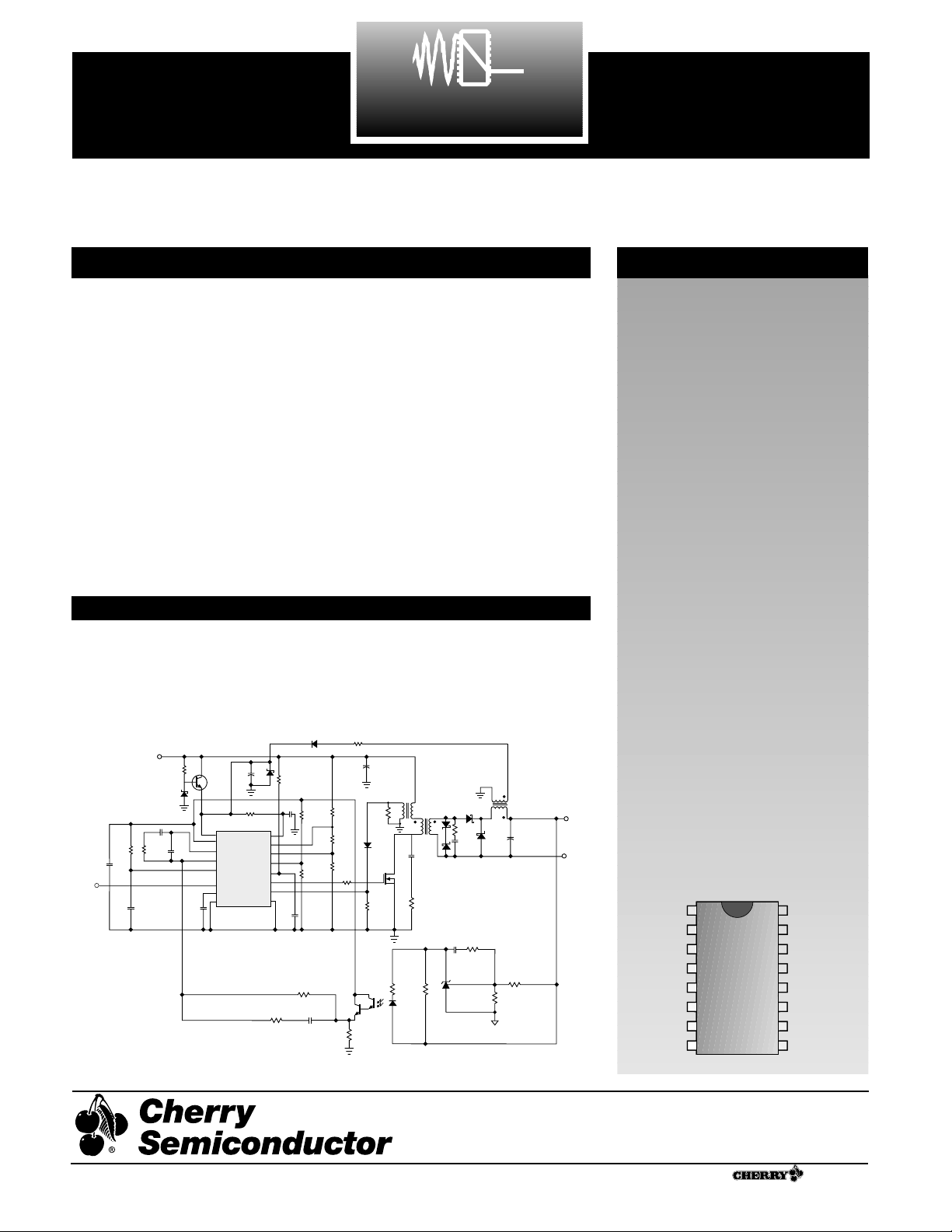
Application Diagram
GATE
I
SENSE
SYNC
FF
UV
OV
R
TCT
I
SET
VC
PGnd
V
CC
LGnd
SS
COMP
V
FB
V
REF
16 Lead SO Narrow & PDIP
1
36V-72V to 5V/5A converter
Rev. 3/26/99
Cherry Semiconductor Corporation
2000 South County Trail, East Greenwich, RI 02818
Tel: (401)885-3600 Fax: (401)885-5786
Email: info@cherry-semi.com
Web Site: www.cherry-semi.com
A Company
®
The CS51221 fixed frequency
feed forward voltage mode
PWM controller contains all of
the features necessary for basic
voltage mode operation. This
PWM controller has been optimized for high frequency primary side control operation. In
addition, this device includes
such features as: Soft Start, accurate duty cycle limit control, less
than 50µA startup current, over
and under voltage protection,
and bidirectional synchronization. The CS51221 is available in
16 lead PDIP and SO narrow
surface mount packages.
V
IN
(36V to 72V)
51k
0.01µF
470pF
20.25k
10
13k
510k
0.1µF
62
IRF634
100
1µF
10
680pF
150
1k
180
MOC81025
2k
100µF
SGnd
V
OUT
(5V/5A)
2200pF
5.1k
0.1µF
SYNC
4.3k
200
10k
1µF
2k
1k
330pF
MBRB2545CT
100pF
10
D11
BAS21
10k
BAS21
18V
22µF
11V
FZT688
10
0.22µF
24.3k
TL431
T1
4:1
T3
100:1
T2
2:5
UV
U1
OV
V
REF
RT/C
T
I
SET
LGnd
SS
V
FB
COMP
SYNC
PGnd
FF
V
C
V
CC
I
SENSE
CS51221/2
GATE
160k
5.6k
D13
V33MLA1206A23
4700pF
1
Page 2

CS51221
Operating Junction Temperature, TJ. . . . . . . . . . . . . . . . . . . . . . . . . . . . . . . . . . . . . . . . . . . . . . . . . . . . . . Internally Limited
Lead Temperature Soldering:
Wave Solder (through hole styles only) . . . . . . . . . . . . . . . . . . . . . . . . . . . . . . . . . . . . . . . . . . 10 Sec. max 260˚C Peak
Reflow (SMD styles only) . . . . . . . . . . . . . . . . . . . . . . . . . . . . . . . . . . . . . . . . . . 60 Sec max. above 183˚C, 230˚C Peak
Storage Temperature Range, TS. . . . . . . . . . . . . . . . . . . . . . . . . . . . . . . . . . . . . . . . . . . . . . . . . . . . . . . . . . . . . . . . -65 to 150˚C
ESD (Human Body Model). . . . . . . . . . . . . . . . . . . . . . . . . . . . . . . . . . . . . . . . . . . . . . . . . . . . . . . . . . . . . . . . . . . . . . . . . . . 2kV
Absolute Maximum Ratings
PIN SYMBOL PIN NAME
V
MAX
V
MIN
I
SOURCE
I
SINK
GATE Gate Drive Output 15V -0.3V 1.0A Peak 1.0A Peak
200mA DC 200mA DC
I
SENSE
Current Sense Input 6V -0.3V 1mA 1mA
R
TCT
Timing Resistor/Capacitor 6V -0.3V 1mA 10mA
FF Feed Forward 6V -0.3V 1mA 25mA
COMP Error Amp Output 6V -0.3V 10mA 20mA
V
FB
Feedback Voltage 6V -0.3V 1mA 1mA
SYNC Sync Input 6V -0.3V 10mA 10mA
UV Under Voltage 6V -0.3V 1mA 1mA
OV Over Voltage 6V -0.3V 1mA 1mA
I
SET
Current Set 6V -0.3V 1mA 1mA
SS Soft Start 6V -0.3V 1mA 10mA
V
CC
Logic Section Supply 15V -0.3V 10mA 50mA
V
C
Power Section Supply 15V -0.3V 10mA 1.0A Peak
200mA DC
V
REF
Reference Voltage 6V -0.3V Internally 10mA
Limited
PGnd Power Ground N/A N/A 1.0A Peak N/A
200mA DC
LGnd Logic Ground N/A N/A N/A N/A
2
Page 3
CS51221
3
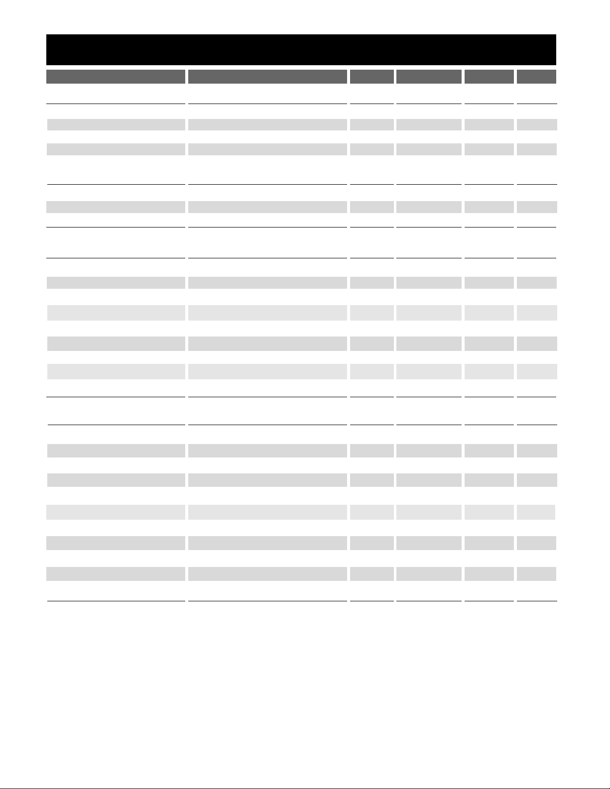
PARAMETER TEST CONDITIONS MIN TYP MAX UNIT
Electrical Characteristics: -40˚C < TA< 85˚C; -40˚C < TJ< 125˚C; 3V < VC < 15V; 4.7V < VCC< 15V; Rt=12K, Ct=390pF
Unless otherwise stated.
■ Start/Stop Voltages
Start Threshold 4.4 4.6 4.7 V
Stop Threshold 3.2 3.8 4.1 V
Hysteresis Start - Stop 400 850 1400 mV
I
CC
@ Startup V
CC
< UVL Start Threshold 38 75 µA
■ Supply Current
I
CC
Operating 9.5 14 mA
I
C
Operating 1nF Load on GATE 12 18 mA
I
C
Operating No switching 2 4 mA
■ Reference Voltage
Total Accuracy 0mA < I
REF
< 2mA 3.2 3.3 3.4 V
Line Regulation 6 20 mV
Load Regulation 0mA < I
REF
< 2mA 6 15 mV
Noise Voltage 10Hz < F < 10kHz (Note 1) 50 µV
Op Life Shift T = 1000Hrs. (Note 1) 4 20 mV
Fault Voltage 2.8 2.95 3.1 V
V
REF(OK)
Voltage 2.9 3.05 3.2 V
V
REF(OK)
Hysteresis 30 100 150 mV
Current Limit 2 40 100 mA
■ Error Amp
Reference Voltage V
FB
= COMP 1.234 1.263 1.285 V
V
FB
Input Current VFB= 1.2V 1.3 2 µA
Open Loop Gain (Note 1) 60 dB
Unity Gain Bandwidth (Note 1) 1.5 MHz
COMP Sink Current COMP = 1.4V, V
FB
= 1.45V 3 12 32 mA
COMP Source Current COMP = 1.4V, V
FB
= 1.15V 1 1.6 2.0 mA
COMP High Voltage V
FB
= 1.15V 2.8 3.1 3.4 V
COMP Low Voltage V
FB
= 1.45V 75 125 300 mV
PSRR Freq = 120Hz (Note 1) 60 85 dB
SS Clamp, V
COMP
SS = 1.4V, V
FB
= 0V, I
SET
= 2V 1.3 1.4 1.5 V
COMP Max Clamp Note 1 1.7 1.8 1.9 V
Page 4
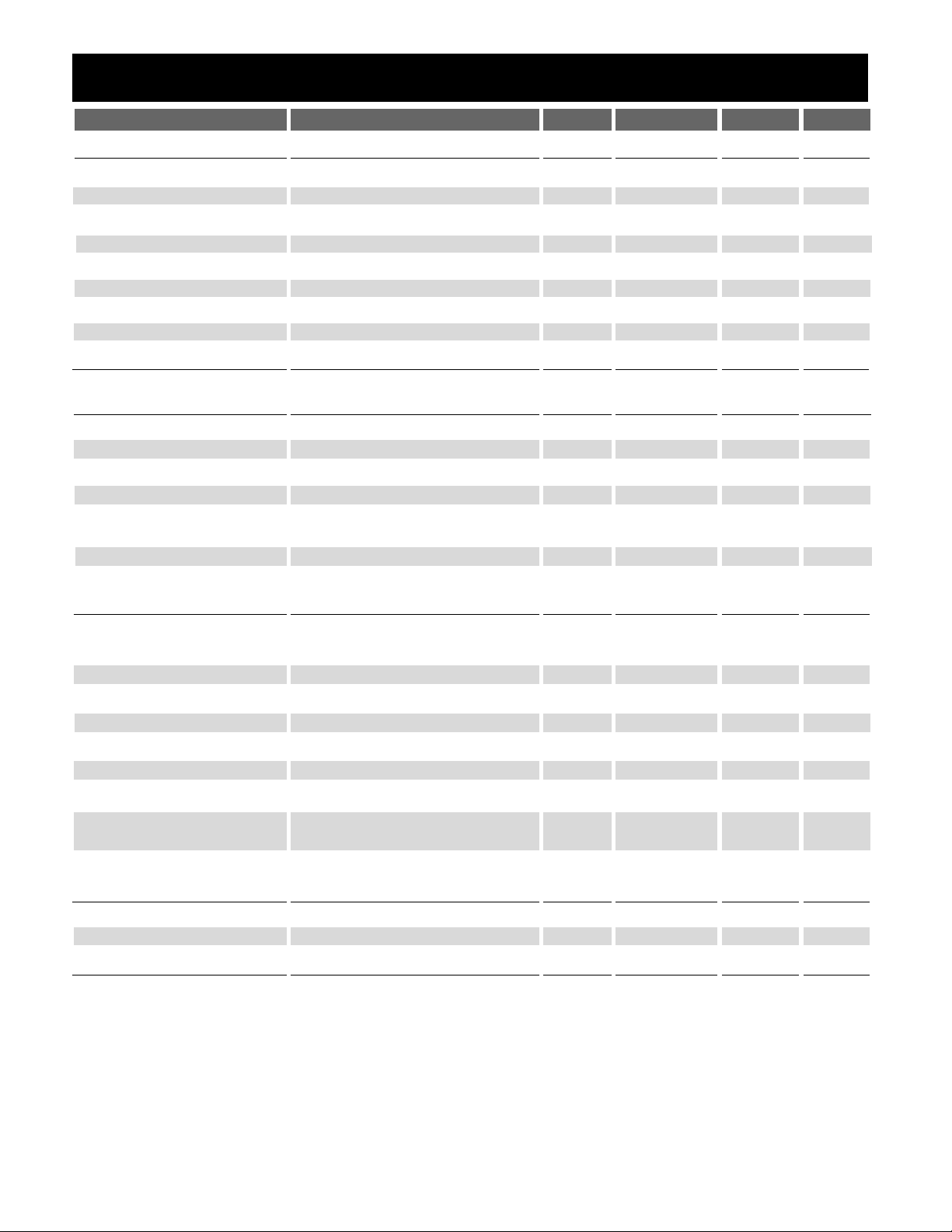
Electrical Characteristics: -40˚C < TA< 85˚C; -40˚C < TJ< 125˚C; 3V < VC < 15V; 4.7V < VCC< 15V; Rt=12K, Ct=390pF
Unless otherwise stated.
CS51221
4
PARAMETER TEST CONDITIONS MIN TYP MAX UNIT
■ Oscillator
Frequency Accuracy 260 273 320 kHz
Voltage Stability 1 2 %
Temperature Stability (Note 1) -40˚C < T
J
< 125˚C8%
Max Frequency (Note 1) 1 MHz
Duty Cycle 80 85 90 %
Peak Voltage (Note 1) 1.94 2.00 2.06 V
Valley Clamp Voltage 0.90 0.95 1.00 V
Valley Voltage (Note 1) 0.85 1.00 1.15 V
Discharge Current 0.85 1.00 1.15 mA
■ Synchronization
Input Threshold 0.9 1.4 1.8 V
Output Pulse Width 200 320 450 ns
Output High Voltage 100µA Load 2.1 2.5 2.8 V
Input Resistance 35 70 140 kΩ
SYNC to Drive Delay Time from SYNC to 100 140 180 ns
GATE Shutdown
Output Drive Current R
SYNC
= 1Ω 1.00 1.50 2.25 mA
■ GATE Driver
High Saturation Voltage V
C
-GATE, VC = 10V, 1.5 2.0 V
I
SOURCE
= 200mA
Low Saturation Voltage GATE-PGnd, I
SINK
= 200mA 1.2 1.5 V
High Voltage Clamp 11.0 13.5 16.0 V
Output Current 1 nF load (Note 1) 1 1.25 A
Output UVL Leakage GATE = 0V 1 50 µA
Rise Time 1nF load, V
C
= 20V, 1V < GATE < 9V 60 100 ns
Fall Time 1nF load, V
C
= 20V, 9V < GATE < 1V 25 50 ns
Max Gate Voltage I
GATE
= 500µA .4 .7 1.0 V
during UVL/Sleep
■ FeedForward (FF)
Discharge Voltage I
FF
= 2mA 0.3 0.7 V
Discharge Current FF = 1V 2 16 30 mA
FF to GATE Delay 50 75 125 ns
Page 5

CS51221
5
PARAMETER TEST CONDITIONS MIN TYP MAX UNIT
■ Overcurrent Protection
Overcurrent Threshold I
SET
= 0.5V, Ramp I
SENSE
0.475 0.500 0.525 V
I
SENSE
to GATE Delay 50 90 125 ns
■ External Voltage Monitors
Overvoltage Threshold OV increasing 1.9 2.0 2.1 V
Overvoltage Hysteresis OV = 2.15V 10.0 12.5 15.0 µA
Current
Undervoltage Threshold UV increasing 0.95 1.00 1.05 V
Undervoltage Hysteresis 25 75 125 mV
■ Soft Start (SS)
Charge Current SS = 2V 40 50 70 µA
Discharge Current SS = 2V 4 5 7 µA
Charge Voltage 2.8 3.0 3.4 V
Discharge Voltage 0.25 0.3 0.35 V
Soft Start Clamp Offset FF = 1.25V 1.15 1.25 1.35 V
Soft Start Fault Voltage OV = 2.15V or LV = 0.85V 0.1 0.2 V
■ Blanking
Blanking Time 50 150 250 ns
SS Blanking Disable V
FB
< 1 2.8 3.0 3.3 V
Threshold
COMP Blanking Disable V
FB
< 1, SS > 3V 2.8 3.0 3.3 V
Threshold
■ Thermal Shutdown
Thermal Shutdown (Note 1) 125 150 180 ˚C
Thermal Hysteresis (Note 1) 5 10 15 ˚C
Note 1: Guaranteed by design, not 100% tested in production.
Electrical Characteristics: -40˚C < TA< 85˚C; -40˚C < TJ< 125˚C; 3V < VC < 15V; 4.7V < VCC< 15V; Rt=12K, Ct=390pF
Unless otherwise stated.
Page 6

Typical Performance Characteristics
6
Package Pin Description
PACKAGE PIN # PIN SYMBOL FUNCTION
Block Diagram
CS51221
3.1V
V
REF
DISABLE
FF Discharge
50µA
V
REF
= 3.3V
OSC
S
R
Q
150ns
Blank
13.5V
SS
PGnd
V
C
GATE
I
SENSE
COMP
V
FB
I
SET
V
REF
V
CC
SYNC
R
TCT
OV
ENABLE
V
BG
FF
Latching
Discharge
1V
UV Monitor
2V
UVL
2mA(maximum load current)
Low
Sat
Gate
Driver
Thermal
Shutdown
+
-
EAMP
I
LIM
G
3
G
4
OV Monitor
Max SS
Det
(Sat Sense)
3.0V
UV
PWM
Comp
VREF OK
UV Lockout
Start/Stop
G
1
3.3V
VO Off
5µA
SS to 1.8V Max
(Sat Sense)
Max Duty Cycle
3.0V
LGnd
2V to 1V Trip Points
Q
(1.263V)
Soft Start Clamp
ON
G2
16L PDIP & 16L SO Narrow
1 GATE External power switch driver with 1.0A peak capability. Rail to
rail output occurs when the capacitive load is between 470pF
and 10nF.
2I
SENSE
Current sense comparator input.
3 SYNC Bidirectional synchronization. Locks to highest frequency.
4 FF PWM ramp.
5 UV Undervoltage protection monitor.
6 OV Overvoltage protection monitor.
7R
T/CT
Timing resistor RTand capacitor CTdetermine oscillator
frequency and maximum duty cycle, D
MAX
.
8I
SET
Voltage at this pin sets pulse-by-pulse overcurrent threshold.
9VFBFeedback voltage input. Connected to the error amplifier
inverting input.
10 COMP Error amplifier output.
11 SS Charging external capacitor restricts error amplifier output
voltage during the power up or fault conditions.
12 LGnd Logic Ground.
13 V
REF
3.3V reference voltage output. Decoupling capacitor can be
selected from 0.01µF to 10µF.
14 V
CC
Logic supply voltage.
15 PGnd Output power stage ground.
16 V
C
Output power stage supply voltage.
Page 7

CS51221
Typical Performance Characteristics
7
Application Information
Feed Forward Voltage Mode Control
In conventional voltage mode control, the ramp signal has
fixed rising and falling slope. The feedback signal is
derived solely from the output voltage. Consequently,
voltage mode control has inferior line regulation and audio
susceptibility.
Feed forward voltage mode control derives the ramp signal from the input line, as shown in Fig.1. Therefore, the
ramp of the slope varies with the input voltage. At the start
of each switch cycle, the capacitor connected to the FF pin
is charged through a resistor connected to the input voltage. Meanwhile, the Gate output is turned on to drive an
external power switching device. When the FF pin voltage
reaches the error amplifier output V
COMP
, the PWM comparator turns off the Gate, which in turn opens the external
switch. Simultaneously, the FF capacitor is quickly discharged to 0.3V.
Overall, the dynamics of the duty cycle are controlled by
both input and output voltages. As illustrated in Fig. 2,
with a fixed input voltage the output voltage is regulated
solely by the error amplifier. For example, an elevated
output voltage reduces V
COMP
which in turn causes duty
cycle to decrease. However, if the input voltage varies, the
slope of the ramp signal will react immediately which provides a much improved line transient response. As an
example shown in Fig.3, when the input voltage goes up,
the rising edge of the ramp signal increases which reduces
duty cycle to counteract the change.
Figure 1: Feed Forward Voltage Mode Control.
The feed forward feature can also be employed to provide
a volt-second clamp, which limits the maximum product
of input voltage and turn on time. This clamp is used in
circuits, such as Forward and Flyback converter, to prevent
the transformer from saturating. Calculations used in the
design of the volt-second clamp are presented in the
Design Guidelines section.
Figure 2: Pulse Width Modulated by Output Current with Constant
Input Voltage.
Figure 3: Pulse Width modulated by Input Voltage with constant
Output Current.
Powering the IC & UVL
The Under Voltage Lockout (UVL) comparator has two
voltage references; the start and stop thresholds. During
power-up, the UVL comparator disables V
REF
(which inturn disables the entire IC) until the controller reaches its
V
CC
start threshold. During power-down, the UVL com-
parator allows the controller to operate until the V
CC
stop
threshold is reached. The CS51221 requires only 50µA during startup. The output stage is held at a low impedance
state in lock out mode.
During power up and fault conditions, the soft-start
clamps the Comp pin voltage and limits the duty cycle.
The power up transition tends to generate temporary duty
cycles much greater than the steady state value due to the
low output voltage. Consequently, excessive current
stresses often take place in the system. Soft Start technique
alleviates this problem by gradually releasing the clamp on
the duty cycle to eliminate the in-rush current. The duration of the Soft Start can be programmed through a capacitance connected to the SS pin. The constant charging current to the SS pin is 50µA (typ).
Theory of Operation
V
OUT
V
IN
R
FF
COMP
C
Power Stage
GATE
Latch & Driver
PWM
Error Amplifier
-
FB
+
+
-
V
OUT
Feedback Network
V
COMP
FF
V
IN
RTC
T
GATE
V
IN
V
COMP
FF
I
OUT
R
TCT
GATE
Page 8

Typical Performance Characteristics
8
Application Information: continued
CS51221
The V
REF
(ok) comparator monitors the 3.3V V
REF
output
and latches a fault condition if V
REF
falls below 3.1V. The
fault condition may also be triggered when the OV pin
voltage rises above 2V or the UV pin voltage falls below
1V. The under-voltage comparator has a built-in hysteresis
of 75mV (typ). The hysteresis for the OV comparator is
programmable through a resistor connected to the OV pin.
When an OV condition is detected, the over-voltage hysteresis current of 12.5µA (typ) is sourced from the pin.
In Fig.4, the fault condition is triggered by pulling the UV
pin to the ground. Immediately, the SS capacitor is discharged with 5µA of current (typ) and the GATE output is
disabled until the SS voltage reaches the discharge voltage
of 0.3V (typ). The IC starts the Soft Start transition again if
the fault condition has recovered as shown in Fig.4.
However, if the fault condition persists, the SS voltage will
stay at 0.10V until the removal of the fault condition.
Figure 4: The fault condition is triggered when the UV pin voltage falls
below 1V. The Soft Start capacitor is discharged and the GATE output
is disabled. CH2: Envelop of GATE output, CH3: SS pin with 0.01µF
capacitor, CH4: UV pin.
Current Sense and Over Current Protection
The current can be monitored by the I
SENSE
pin to achieve
pulse by pulse current limit. Various techniques, such as a
using current sense resistor or current transformer, can be
adopted to derive current signals. The voltage of the I
SET
pin sets the threshold for maximum current. As shown in
Fig. 5, when the I
SENSE
pin voltage exceeds the I
SET
voltage,
the current limit comparator will reset the GATE latch flipflop to terminate the GATE pulse.
Figure 5: The GATE output is terminated when the I
SENSE
pin voltage
reaches the threshold set by the I
SET
pin. CH2: I
SENSE
pin, CH4: I
SET
pin,
CH3: GATE pin
The current sense signal is prone to leading edge spikes
caused by the switching transition. A RC low-pass filter is
usually applied to the current signals to avoid premature
triggering. However, the low pass filter will inevitably
change the shape of the current pulse and also add cost.
The CS51221uses leading edge blanking circuitry that
blocks out the first 150ns (typ) of each current pulse. This
removes the leading edge spikes without altering the current waveform. The blanking is disabled during Soft Start
and when the V
COMP
is saturated high so that the minimum on-time of the controller does not have the additional
blanking period. The max SS detect comparator keeps the
blanking function disabled until SS charges fully. The output of the max Duty Cycle detector goes high when the
error amplifier output gets saturated high, indicating that
the output voltage has fallen well below its regulation
point and the power supply may be under load stress.
Oscillator and Synchronization
The switching frequency is programmable through a RC
network connected to the R
TCT
Pin. As shown in Fig.6,
when the R
TCT
pin reaches 2V, the capacitor is discharged
by a 1mA current source and the Gate signal is disabled.
When the R
TCT
pin decreases to 1V, the Gate output is
turned on and the discharge current is removed to let the
RTCTpin ramp up. This begins a new switching cycle. The
CT charging time over the switch period sets the maximum
duty cycle clamp which is programmable through the R
T
value as shown in the Design Guidelines. At the beginning
of each switching cycle, the SYNC pin generates a 2.5V,
320nS (typ) pulse. This pulse can be utilized to synchronize
other power supplies.
Page 9

CS51221
Typical Performance Characteristics
9
Application Information: continued
Figure 6: The Sync pin generates a sync pulse at the beginning of each
switching cycle. CH2: GATE Pin, CH3: R
TCT,
CH4: SYNC pin.
The bi-directional SYNC pin can also receive an external
sync signal of a greater frequency. As show in Fig.7, when
the SYNC pin is triggered by an incoming signal, the IC
immediately discharges CT. The GATE signal is turned on
once the RTCTpin reaches the valley voltage. Because of
the steep falling edge, this valley voltage falls below the
regular 1V threshold. However, the RTCT pin voltage is
then quickly raised by a clamp. When the RTCTpin reaches
the 0.95V(typ) Valley Clamp Voltage, the clamp is disconnected after a brief delay and CT is charged through RT.
Figure 7: Operation with external sync. CH 2: SYNC pin, CH3: Gate pin,
G4: R
TCT
pin.
Switch Frequency and Maximum Duty Cycle Calculations
Oscillator timing capacitor, C
T
, is charged by V
REF
through
R
T
and discharged by an internal current source. During
the discharge time, the internal clock signal sets the Gate
output to the low state, thus providing a user selectable
maximum duty cycle clamp. Charge and discharge times
are determined by following general formulas;
t
C
= RTCTln
t
d
= RTCTln
,
where
t
C
= charging time;
t
d
= discharging time;
V
VALLEY
= valley voltage of the oscillator;
V
PEAK
= peak voltage of the oscillator.
Substituting in typical values for the parameters in the
above formulas:
V
REF
= 3.3V, V
VALLEY
= 1V, V
PEAK
= 2V, Id= 1mA
tC= 0.57RTC
T
td= RTCTln
D
max
=
0.57
0.57+ In
It is noticed from the equation that for the oscillator to
function properly, R
T
has to be greater than 2.3k.
)
1.3 - 0.001R
T
2.3- 0.001R
T
(
)
1.3 - 0.001R
T
2.3- 0.001R
T
(
)
(V
REF
- V
PEAK
- IdRT)
(V
REF
- V
VALLEY
- IdRT)
(
)
(V
REF
- V
VALLEY
)
(V
REF
- V
PEAK
)
(
Design Guidelines
Page 10

Application Information: continued
10
CS51221
Figure 8: Typical Performance Characteristics: Oscillator frequency vs
C
T
Figure 9: Typical Performance Characteristics: Oscillator duty cycle vs
R
T
Select RC for Feed Forward Ramp
If the line voltage is much greater than the FF pin Peak
Voltage, the charge current can be treated as a constant and
is equal to V
IN
/R. Therefore, the volt-second value is deter-
mined by:
V
IN
× T
ON =
(
V
COMP
− V
FF(d)
)
× R × C
where V
COMP
= COMP pin voltage
V
FF(d)
= FF pin discharge voltage.
As shown in the equation, the volt-second clamp is set by
the V
COMP
clamp voltage which is equal to 1.8V. In
Forward or Flyback circuits, the volt-second clamp value is
designed to prevent transformers from saturation.
In a buck or forward converter, volt-second is equal to
V
IN
× T
ON ≈
n = transformer turns ratio
which is a constant determined by the regulated output
voltage, switching period and transformer turns ration (use
1 for buck converter). It is interesting to notice from the
aforementioned two equations that during steady state,
V
COMP
doesn’t change for input voltage variations. This
intuitively explains why FF voltage mode control has superior line regulation and line transient response. Knowing
the nominal value of VINand TON, one can also select the
value of RC to place V
COMP
at the center of its dynamic
range.
Select Feedback Voltage Divider
As shown in Fig.10, the voltage divider output feeds to the
FB pin, which connects to the inverting input of the error
amplifier. The non-inverting input of the error amplifier is
connected to a 1.27V (typ) reference voltage. The FB pin
has an input current which has to be considered for accurate DC outputs. The following equation can be used to
calculate the R1 and R2 value
V
OUT
= 1.27 − ∇
where ∇ is the correction factor due to the existence of the
FB pin input current Ier.
∇ = (Ri + R1//R2)Ier
Ri = DC resistance between the FB pin and the voltage
divider output.
Ier = V
FB
input current, 1.3µA typical.
)
R2
R1 + R2
(
)
V
OUT
× T
S
n
(
800000
700000
600000
500000
400000
Frequency
300000
200000
100000
1
0.95
0.9
0.85
0.8
0.75
0.7
0.65
0.6
0.55
0.5
1000
0
0.0001
10K
50K
10000
RT = 5K
0.001
CT (µF)
100000
1000000
0.01
Page 11

Application Information: continued
CS51221
Figure 10. The design of feedback voltage divider has to consider the
error amplifier input current.
Design voltage dividers for OV and UV detection
In Fig.11, the voltage divider uses three resistors in series
to set OV and UV threshold seen from the input voltage.
The values of the resistors can be calculated from the following three equations, where the third equation is
derived from OV hysteresis requirement.
V
IN(LOW)
× = 1V (A)
V
IN(HIGH)
× = 2V (B)
12.5µA × (R1 + R2) = V
HYST
(C)
where
V
LINE(LOW)
, V
LINE(HIGH)
= input voltage OV and UV threshold
V
HYST
= OV hysteresis seen at V
IN
It is self-evident from equation A and B that to use this
design, V
IN(HIGH)
has to be two times greater than
V
IN(LOW)
. Otherwise, two voltage dividers have to be used
to program OV and UV separately.
Figure 11. OV/UV Monitor Divider.
)
R3
R2 + R3 + R1
(
)
R2 + R3
R2 + R3 + R1
(
11
V
OUT
Ier
-
COMP
+
Ri
+
-
1.27
R1
FB
R2
V
IN
R
1
V
R
UV
V
OV
R
3
2
Page 12

Package Specification
Thermal Data 16L SO 16L
Narrow PDIP
R
ΘJC
typ 28 42 ˚C/W
R
ΘJA
typ 115 80 ˚C/W
12
Rev. 3/26/99 © 1999 Cherry Semiconductor Corporation
D
Lead Count Metric English
Max Min Max Min
16L SO Narrow 10.00 9.80 .394 .386
16L PDIP 19.69 18.67 .775 .735
Ordering Information
Part Number Description
CS51221ED16 16L SO Narrow
CS51221EDR16 16L SO Narrow (tape & reel)
CS51221EN16 16L PDIP
CS51221
PACKAGE DIMENSIONS IN mm (INCHES)
PACKAGE THERMAL DATA
Cherry Semiconductor Corporation reserves the right to
make changes to the specifications without notice. Please
contact Cherry Semiconductor Corporation for the latest
available information.
Surface Mount Narrow Body (D); 150 mil wide
Plastic DIP (N); 300 mil wide
0.39 (.015)
MIN.
2.54 (.100) BSC
1.77 (.070)
1.14 (.045)
D
Some 8 and 16 lead
packages may have
1/2 lead at the end
of the package.
All specs are the same.
.203 (.008)
.356 (.014)
REF: JEDEC MS-001
3.68 (.145)
2.92 (.115)
8.26 (.325)
7.62 (.300)
7.11 (.280)
6.10 (.240)
.356 (.014)
.558 (.022)
1.27 (.050) BSC
0.51 (.020)
0.33 (.013)
6.20 (.244)
5.80 (.228)
4.00 (.157)
3.80 (.150)
1.57 (.062)
1.37 (.054)
D
0.25 (0.10)
0.10 (.004)
1.75 (.069) MAX
1.27 (.050)
0.40 (.016)
REF: JEDEC MS-012
0.25 (.010)
0.19 (.008)
 Loading...