

Page 1
Features
■ Programmable Fixed
Frequency
■ Programmable FET Non-
overlap
■ Enable Lead
■ 12V Fixed Auxiliary
Supply Control
■ Under and Overvoltage
Shutdown
■ Output Undervoltage
Protection with Timer
■ Master/Slave Clock
Syncing Capability
■ Sync Frequency Range
Detection
■ 80ns PWM Propagation
Delay
■ 20mA 5V Reference
Output
■ Small 24 lead SSOP
Package
■ Controlled Hiccup Mode
Package Options
CS5106
Multi-Feature, Synchronous plus Auxiliary
PWM Controller
CS5106
Description
The CS5106 is a fixed frequency,
current mode controller with one
single NFET driver and one dual
FET, synchronous driver. The synchronous driver allows for
increased efficiency of the main isolated power stage and the single
driver allows the designer to develop auxiliary supplies for controller
power as well as secondary side
house keeping. In addition,
because the synchronous drivers
have programmable FET non-overlap, the CS5106 is an ideal controller for soft-switched converter
topologies.
The CS5106 is specifically designed
for isolated topologies where speed,
flexibility, reduced size and
reduced component count are
requirements. The controller contains the following features:
Undervoltage Shutdown,
Overvoltage Shutdown,
Programmable Frequency,
Programmable Synchronous NonOverlap Time, Master/Slave
Clocking with Frequency Range
Detection, Enable, Output
Undervoltage Protection with
Timer, 20mA 5V Output, 80ns
PWM propagation delay, and
Controlled Hiccup Mode.
The CS5106 has junction temperature and supply ranges of -40ûC to
125ûC and 9V to 16V respectively
and is available in the 24 lead SSOP
package.
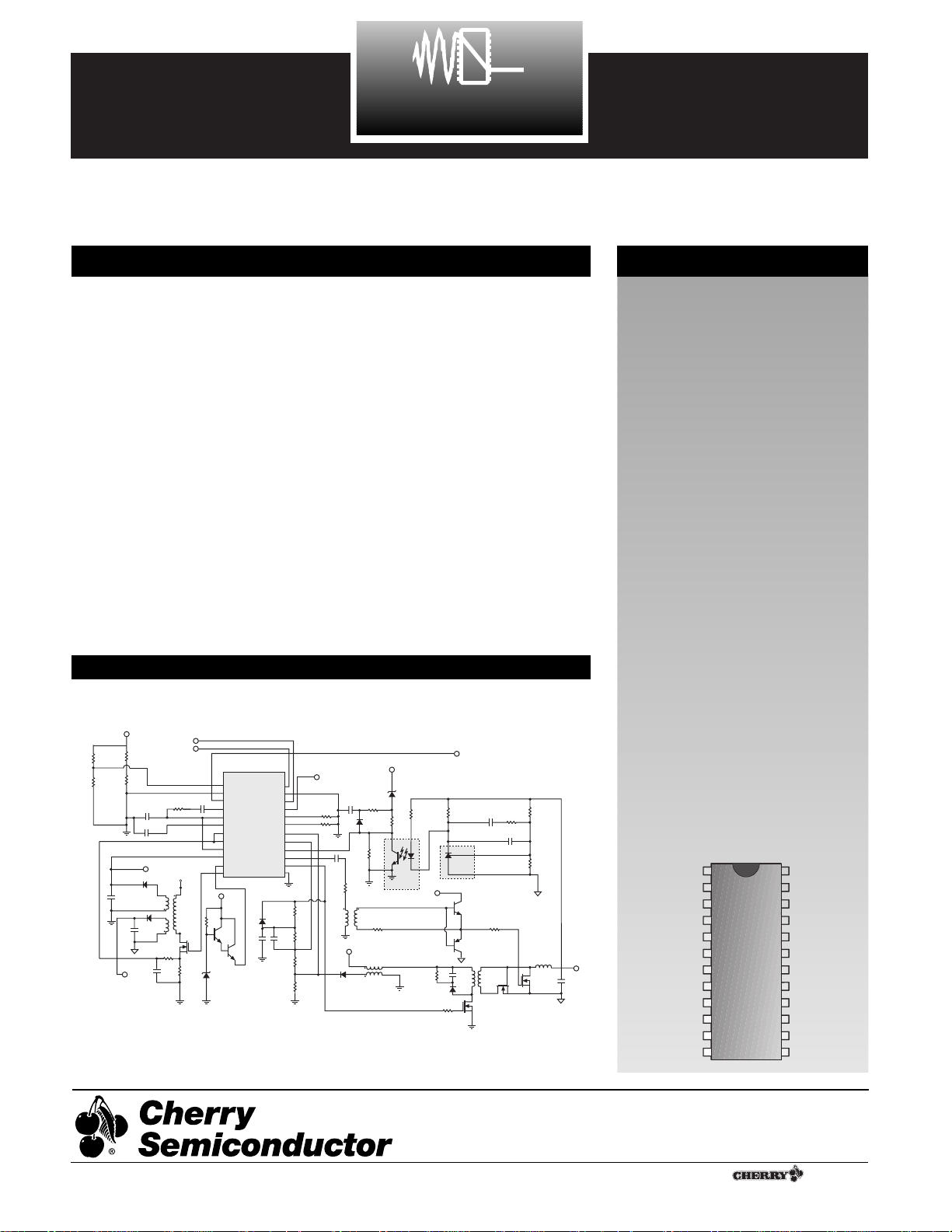
Applications Diagram
24 Lead SSOP
1
UVSD
OVSD
OAM
OAOUT
V
5REF
OUVDELAY
I
LIM1
RAMP1
V
FB1
V
SS
V
CC
GATE1
ENABLE
PROGRAM
SYNC
IN
SYNC
OUT
FADJ
DLYSET
I
LIM2
RAMP2
V
FB2
V
DD
GATE2B
GATE2
Rev. 10/27/98
48V to 3.3V Forward Converter with Synchronous Rectifiers
Cherry Semiconductor Corporation
2000 South County Trail, East Greenwich, RI 02818
Tel: (401)885-3600 Fax: (401)885-5786
Email: info@cherry-semi.com
Web Site: www.cherry-semi.com
A Company
¨
V
IN
C5
V
C1
C2
V
D1
D2
AUXS
SYNC
ENABLE
R4
AUXP
V
T1
R5
C7
IN
CS5106
UVSD
ENABLE
PROGRAM
OVSD
V
SYNC
5REF
C3
IN
V
R8
Q1
R6
IN
D6
OAM
OA
OUVDELAY
I
LIM1
RAMP1
V
V
V
GATE1
Q2
SYNC
OUT
FADJ
OUT
DLYSET
I
LIM2
RAMP2
V
FB1
FB2
GATE2B
SS
GATE2
CC
V
D3
C10
C9
R27
R1
R2
R3
C4
V
R13
AUXP
OUT
D5
C6
R7
R20
R15
D8
R14
C8
CNY17-4
T4
R26
V
IN
T3
D4
R23
SYNC
IN
R24
R25
DD
R9
R10
R11
R12
V
5REF
R21
R18
R17
C13
R19
L1
Q5
Q4
R16
C14
TL431
V
AUXS
Q7
Q6
T2
C11
D7
Q3
R22
V
MAIN
C12
1
Page 2

CS5106
2
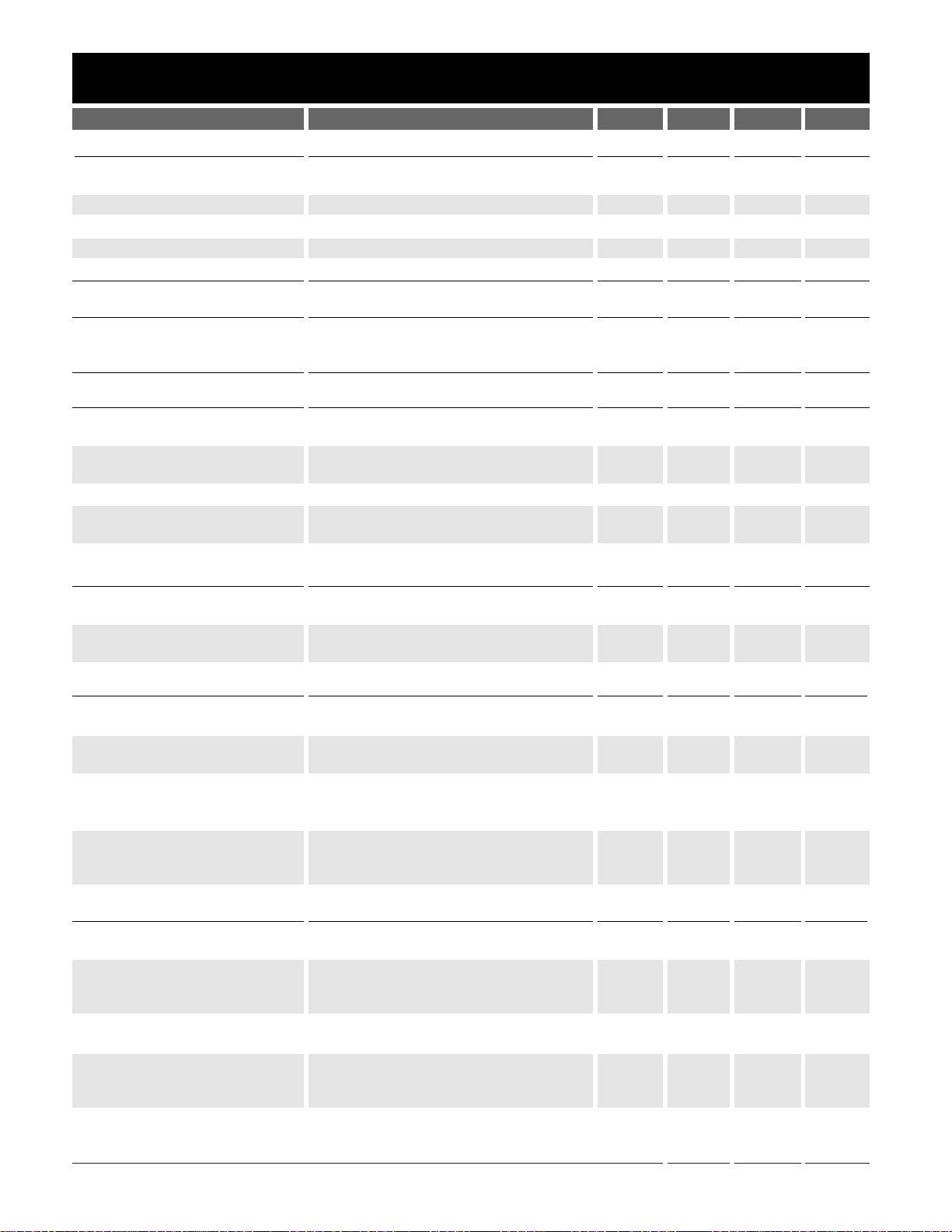
Absolute Maximum Ratings
Lead Symbol Lead Name
V
MAX
V
MIN
I
SOURCE
I
SINK
UVSD Undervoltage Shutdown Input 6V -0.3V 1mA N/A
OVSD Overvoltage Shutdown Input 6V -0.3V 1mA N/A
V
5REF
5V Reference Output 6V -0.3V 150mA 25mA
OAM Error Amp Minus Input 6V -0.3V 250µA 1.2mA
OAOUT Error Amp Output 6V -0.3V 300µA 100mA
OUVDELAY Output Overcurrent Timer Capacitor 6V -0.3V 15µA N/A
I
LIM1
Auxiliary Primary Side Current Limit Input 6V -0.3V 10µA N/A
RAMP1 Auxiliary Primary Side Current Ramp Input 6V -0.3V 10µA N/A
V
FB1
Auxiliary Voltage Feedback Input 6V -0.3V 5µA 100µA
V
SS
Bootstrapped Power Input 20V -0.3V 2µA 0.5A Peak
300mA DC
V
CC
Main Power Input 20V -0.3V See Note 1 0.5A Peak
300mA DC
GATE1 Auxiliary FET Driver Output 20V -0.3V 0.5A Peak 0.5Peak
100mA DC 100mA DC
Gnd Ground 0V 0V 0.5A Peak N/A
300mA DC
GATE2 Synchronous FET Driver Output 20V -0.3V 0.5A Peak 0.5APeak
100mA DC 100mA DC
GATE2B Synchronous FET Driver Output B 20V -0.3V 0.5A Peak 0.5A Peak
100mA DC 100mA DC
V
FB2
Synchronous Voltage Feedback Input 6V -0.3V 10µA 100µA
RAMP2 Synchronous Primary Side Current Ramp Input 6V -0.3V 10µA N/A
I
LIM2
Synchronous Primary Side Current Limit Input 6V -0.3V 10µA N/A
DLYSET Gate Non-Overlap Programming Input 2.5V -0.3V 125µA N/A
FADJ Frequency Programming Input 2.5V -0.3V 125µA N/A
SYNC
OUT
Clock Master Output 6V -0.3V 50mA 100mA
SYNC
IN
Clock Slave Input 6V -0.3V N/A 1mA
PROGRAM Enable Programming Input 16V -0.3V 30µA N/A
ENABLE Enable Input 16V -0.3V 300µA N/A
Note 1: Current out of V
CC
is not limited. Care should be taken to prevent shorting VCCto Ground.
Operating Junction Temperature, TJ..................................................................................................................................... 150¡C
Operating Temperature Range, TA...............................................................................................................................-40 to 85¡C
Storage Temperature Range, TS...................................................................................................................................-65 to 150¡C
ESD (Human Body Model).........................................................................................................................................................2kV
Lead Temperature Soldering: Reflow (SMD styles only).............................................60 sec. max above 183¡C, 230¡C peak
Page 3

CS5106
3
PARAMETER TEST CONDITIONS MIN TYP MAX UNIT
Electrical Characteristics: TJ = -40¡C to 125¡C, V
SS
= 9 to 16V, V
5REFILOAD
= 2mA, SYNC
OUT
Free Running, unless other-
wise specified. For All Specs: UVSD=6V, OVSD = 0V, ENABLE = 0V, I
LIM(1,2)
= 0,V
FB(1,2)
= 3V,R
FADJ
= R
DLYSET
= 27.4k½.
■ V
SS
Supply Current Measure current into VSSwhen 16.00 23.00 mA
V
5REFILOAD
=0mA. 9V ² VSS² 13V.
Measure current into VSSwhen 16.00 25.00 mA
V
5REFILOAD
=0mA. 13V < VSS² 16V.
Measure current into VSSwhen 16.00 30.00 mA
V
5REFILOAD
=0mA. 16V < VSS² 20V.
■ Low V
CC
Supply Current Float VSS. Set VCC=7V & measure 1.50 3.50 mA
VCCcurrent while V
5REFILOAD
=0mA.
■ V
SS
TO VCCDIODE
Diode ON Voltage Measure VSS- VCC. 0.20 0.75 1.00 V
■ Reference
5V Internal Voltage Reference Measure V
REF
voltage when 4.85 5.00 5.15 V
I
REF
=0 and I
REF
=20 mA.
V
REF
OK Threshold Adjust V
REF
from 4.8V-4.0V until 4.30 4.55 4.70 V
PWM1,2 goes low.
■ Low V
CC
Lockout
VCCTurnon Threshold Voltage VCCincreasing until ICC> 3.5mA 7.00 7.25 7.50 V
V
5REFILOAD
= 0mA
VCCTurnoff Threshold Voltage VCCdecreasing until ICC< 3.5mA 6.30 6.70 7.10 V
V
5REFILOAD
= 0mA
Hysteresis Turnon - Turnoff 0.40 0.55 0.70 V
■ Clock
Operating Frequency1 Measure frequency from SYNC
OUT
. 485.0 512.0 540.0 kHz
SYNCINInput Impedance Measure input impedance. 7.00 15.00 k½
SYNC
OUT
Output Low Voltage R
LOAD
= 2k½ to V
5REF
1.00 1.50 V
SYNC
OUT
Output High R
LOAD
= 2k½ to Gnd 3.50 4.20 V
Voltage
SYNCINDetect Frequency Verify SYNC
OUT
= SYNCIN, 425.0 555.0 kHz
R
LOAD
= 2k½ to Gnd
Max. Low SYNC Rej. Frequency Verify SYNC
OUT
= FCLK when 340.0 kHz
R
LOAD
= 2k½ to Gnd.
Min. High SYNC Rej. Frequency Verify SYNC
OUT
= FCLK when 690 kHz
R
LOAD
= 2k½ to Gnd.
SYNCINInput Threshold Functional Testing 0.90 1.85 2.90 V
Voltage Verify FCLK from 1.0V to 2.8V.
Main PWM Clock Pulse (GBD) - CLPH1
Width One Shot Pulse Width 80.0 100.0 120.0 ns
Aux PWM Clock Pulse (GBD) -CLPH2
Width One Shot Pulse Width 80.0 100.0 120.0 ns
■ Bias Supply Error Amplifier
Output Low Voltage V
SS
> 12.6V. Measure OAOUT 43.0 85.0 mV
voltage when sinking 1.0 mA.
Output High Voltage V
SS
< 11.4V. Measure OAOUT 4.55 4.75 V
voltage when sourcing 150µA.
Output High Source Current V
SS
< 11.4V. Measure OAOUT source 150.0 225.0 300.0 µA
current when OAOUT = 0.5V.
Page 4
CS5106
4
PARAMETER TEST CONDITIONS MIN TYP MAX UNIT
Electrical Characteristics: TJ = -40¡C to 125¡C, V
SS
= 9 to 16V, V
5REFILOAD
= 2mA, SYNC
OUT
Free Running, unless other-
wise specified. For All Specs: UVSD=6V, OVSD = 0V, ENABLE = 0V, I
LIM(1,2)
= 0,V
FB(1,2)
= 3V,R
FADJ
= R
DLYSET
= 27.4k½.
■ Bias Supply Error Amplifier: continued
Output Low Sink Current V
SS
> 12.6V. Measure OAOUT sink 3.0 20.0 50.0 mA
current when OAOUT = 2.5V.
VSSSet Point Adjust VSSuntil OAOUT goes low. 11.60 12.25 12.80 V
Large Signal Gain (GBD) 15.00 V/mV
Unity Gain Bandwidth (GBD) 1.00 MHz
Common Mode Input Range (GBD) 1.00 2.00 V
■ V
SS
Voltage
VSSReset Voltage Toggle ENABLE between Gnd & VCC,
then adjust VSSfrom 2.0V-0.8V until
OAOUT goes high. 1.00 1.40 1.80 V
■ Undervoltage Lockout
UVSD Turn On Adjust UVSD from 4.7V-5.3V 4.80 5.00 5.10 V
Threshold Voltage until GATE 1, 2 goes high.
UVSD Turn Off Threshold Adjust UVSD from 5.1V-4.3V 4.45 4.70 4.95 V
Voltage until GATE 1, 2 goes low.
Hysteresis Turnon - Turnoff 0.20 0.27 0.40 V
UVSD Input Bias Current Set UVSD=0V. Measure Current 0.20 0.50 µA
out of UVSD lead.
■ Overvoltage Lockout
OVSD Threshold Voltage Adjust OVSD from 4.7V-5.3V 4.85 5.00 5.15 V
until GATE 1, 2 goes low.
OVSD Input Bias Current Set OVSD=0V. Measure Current out 0.20 0.50 µA
of OVSD lead.
■ ENABLE & PROGRAM
ENABLE Lead Output Current Measure current out of 100.0 266.0 500.0 µA
ENABLE when ENABLE = 0V.
PROGRAM Lead Output Measure current out of 20.0 60.0 100.0 µA
Current PROGRAM when PROGRAM = 0V.
PROGRAM Threshold ENABLE = Gnd. Adjust 1.20 1.40 1.60 V
Voltage PROGRAM from 1.0V - 1.8V
until GATE 1, 2 goes high.
ENABLE Threshold Voltage PROGRAM = Gnd. 1.20 1.40 1.60 V
Adjust ENABLE from 1.0V - 1.8V
until GATE 1, 2 goes high.
■ Output Undervoltage Delay
OUVDELAY Charging Set OUVDELAY = 1V, V
FB1
= 4.4V 7.50 10.00 12.50 µA
Current Measure OUVDELAY I
CHARGE
.
OUVDELAY Latchoff Voltage Toggle ENABLE between Gnd & VCC, 4.80 5.00 5.20 V
then adjust OUVDELAY from
4.7V - 5.3V until GATE 1, 2, goes low.
OUVDELAY Set Current OUVDELAY = VOCLO + 50mV 0.50 1.00 mA
Measure current into OUVDELAY.
V
FB1
Charge Threshold VSS=1V. Toggle ENABLE between 4.05 4.22 4.40 V
Gnd & VCC, adjust V
FB1
from 3.8V - 4.6V
until GATE 1, 2 goes low.
V
FB2
Charge Threshold V
SS
= 1V. Toggle ENABLE between 3.90 4.15 4.35 V
Gnd & VCC, adjust V
FB2
from 3.8V - 4.6V
until GATE 1, 2 goes low.
Page 5

PARAMETER TEST CONDITIONS MIN TYP MAX UNIT
CS5106
5
Electrical Characteristics: TJ = -40¡C to 125¡C, V
SS
= 9 to 16V, V
5REFILOAD
= 2mA, SYNC
OUT
Free Running, unless other-
wise specified. For All Specs: UVSD=6V, OVSD = 0V, ENABLE = 0V, I
LIM(1,2)
= 0,V
FB(1,2)
= 3V,R
FADJ
= R
DLYSET
= 27.4k½.
■ Current Limit Circuits
I
LIM1
Current Limit Threshold Adjust I
LIM1
from 1.0V - 1.3V until 1.16 1.24 1.30 V
Voltage GATE1 goes low.
I
LIM1
Short Circuit Threshold Adjust I
LIM1
from 1.30V - 1.50V until 1.35 1.44 1.51 V
Voltage GATE1 skips 2-cycles with reference
to SYNC
OUT.
I
LIM1
Input Bias Current Set I
LIM1
=0V. Measure current 0.50 5.00 µA
out of I
LIM1
lead.
I
LIM2
Current Limit Adjust I
LIM2
from 1.0V - 1.3V until 1.16 1.24 1.30 V
Threshold V GATE2 goes low.
I
LIM2
Short Circuit Adjust I
LIM2
from 1.30V - 1.50V until 1.35 1.44 1.51 V
Threshold Voltage GATE2 skips 2-cycles with reference
to SYNC
OUT
.
I
LIM2
Input Bias Current Set I
LIM 2
= 0V. Measure current out 0.50 5.00 µA
of I
LIM2
lead.
■ Voltage Feedback Control
RAMP1 Offset Voltage V
FB1
=0V. Adjust RAMP1 from 0V - 0.3V 0.08 0.13 0.20 V
until GATE1 goes low. Measure V
RAMP1
.
RAMP1 Input Bias Current Set RAMP1 = 0V. Measure Current 0.50 5.00 µA
out of RAMP1 lead.
RAMP2 Offset Voltage V
FB2
= 0V. Adjust RAMP2 from 0.08 0.13 0.20 V
0V-3V until GATE2 goes low.
Measure V
RAMP2
.
RAMP2 Input Bias Current Set RAMP2 = 0V. Measure Current
out of RAMP2 lead. 0.50 5.00 µA
V
FB1
Input Impedance Measure input impedance. 60.0 120.0 220.0 k½
V
FB2
Input Impedance Measure Input impedance. 60.0 120.0 220.0 k½
■ Gate1,2,2B Output Voltages V
SS
= 12V. V
CC
= V
SS
- V
DON
GATE1 Low State PROGRAM = 0V. Measure GATE1 0.15 0.80 V
voltage when sinking 1mA.
GATE2 Low State PROGRAM = 0V. Measure GATE2 0.18 0.80 V
voltage when sinking 1mA.
GATE2B Low State PROGRAM = 0V. Measure GATE2B 0.18 0.80 V
voltage when sinking 1mA.
GATE2B High State Measure V
CC
- GATE2B voltage 1.65 2.00 V
when sourcing 1mA.
GATE2 High State Measure VCC- GATE2 voltage 1.65 2.00 V
when sourcing 1mA.
GATE1 High State Measure V
CC
- GATE1 voltage 1.65 2.00 V
when sourcing 1mA.
■ Propagation Delays
I
LIM1
Delay to Output GATE1 Measure delay from I
LIM1
going 80.0 120.0 ns
high to GATE1 going low.
I
LIM2
Delay to Output GATE2 Measure delay from I
LIM2
going 80.0 100.0 ns
high to GATE2 going low.
RAMP1 Delay to Output GATE1 Measure delay from RAMP1 going 80.0 115.0 ns
high to GATE1 going low.
RAMP2 Delay to Output GATE2 Measure delay from RAMP2 going 80.0 100.0 ns
high to GATE2 going low.
Page 6

Package Lead Description
CS5106
6
PARAMETER TEST CONDITIONS MIN TYP MAX UNIT
Electrical Characteristics: TJ = -40¡C to 125¡C, V
SS
= 9 to 16V, V
5REFILOAD
= 2mA, SYNC
OUT
Free Running, unless other-
wise specified. For All Specs: UVSD=6V, OVSD = 0V, ENABLE = 0V, I
LIM(1,2)
= 0,V
FB(1,2)
= 3V,R
FADJ
= R
DLYSET
= 27.4k½.
PACKAGE LEAD # LEAD SYMBOL FUNCTION
■ GATE 2, 2B Non-Overlap Delay
GATE2 Turn-on Delay Measure delay from GATE2B going low 20.0 45.0 70.0 ns
from GATE2B @1.7V to GATE2 going high @1.7V.
GATE2B Turn-on Delay Measure delay from GATE2 going low 20.0 45.0 70.0 ns
from GATE2 @1.7V to GATE2B going high @1.7V.
■ GATE 1, 2, 2B Rise & Fall Times V
SS
=12V,VCC=VSS-V
DON
GATE1 Rise Time Measure GATE1 Rise Time from 50.0 80.0 ns
90% to 10%. C
LOAD
= 150pF.
GATE1 Fall Time Measure GATE1 Fall Time from
10% to 90%. C
LOAD
= 150pF. 30.0 60.0 ns
GATE2 Rise Time Measure GATE2 Rise Time from
90% to10%. C
LOAD
= 50pF. 50.0 80.0 ns
GATE2 Fall Time Measure GATE2 Fall Time from
10% to 90%. C
LOAD
= 50pF. 15.0 30.0 ns
GATE2B Rise Time Measure GATE2B Rise Time from
90% to10%. C
LOAD =
50pF. 50.0 80.0 ns
GATE2B Fall Time Measure GATE2B Fall Time from
10% to 90%. C
LOAD
= 50pF. 15.0 30.0 ns
1 UVSD Undervoltage shutdown lead. Typically this lead is connected through a
resistor divider to the main high voltage (VIN) line. If the voltage on this lead
is less than 5V then a fault is initiated such that GATE1, GATE2 and GATE2B
go low.
2 OVSD Overvoltage shutdown lead. Typically this lead is connected through a resistor
divider to the main high voltage (VIN) line. If the voltage on this lead exceeds
5V then a fault is initiated such that GATE1, GATE2 and GATE2B go low.
3V
5REF
5V reference output lead. Capable of 20mA nominal output. If this lead falls
to 4.5V, a fault is initiated such that GATE1, GATE2 and GATE2B go low.
4 OAM Auxiliary error amplifier minus input. This lead is compared to 1.2V nominal
on the auxiliary error amp plus lead and represents the VSSvoltage divided
by ten.
5 OAOUT Auxiliary error amplifier output lead. Source current 300µA max.
6 OUVDELAY Output undervoltage timing capacitor lead. If the controlled output voltages
of either the main or the auxiliary supply are such that either V
FB1
or V
FB2
is
greater that 4.1V nominal, then capacitor from OUVDELAY to ground will
begin charging. If the over voltage duration is such that the OUVDELAY
voltage exceeds 5V, then a fault will be initiated such that GATE1, GATE2
and GATE2B will go low.
7I
LIM1
Pulse by pulse over current protection lead for the auxiliary PWM. A voltage
exceeding 1.2V nominal on I
LIM1
will cause GATE1 to go low. A voltage
exceeding 1.4V nominal on I
LIM1
will cause GATE1 to go low for at least two
clock cycles.
8 RAMP1 Current Ramp Input Lead for the Auxiliary PWM. A voltage which is linear
with respect to current in the primary side of the auxiliary trans former is
usually represented on this lead. A voltage exceeding V
FB1
- 0.13 on RAMP1
will cause GATE1 to go low.
Page 7

CS5106
7
PACKAGE LEAD # LEAD SYMBOL FUNCTION
Package Lead Description: continued
9V
FB1
Voltage Feedback Lead for the Auxiliary PWM. A voltage which represents
the auxiliary power supply output voltage is fed to this lead. A voltage less
than RAMP1+0.13 on V
FB1
will cause GATE1 to go low.
10 V
SS
VSSpower/feedback input lead. See VCCfor description of power operation.
In addition, this lead is fed to a divide by ten resistor divider and compared to
1.2V nominal at the positive side of the error amplifier.
11 V
CC
V
CC
power input lead. This input runs off a Zener referenced supply until
VSS> VCC. Then an internal diode which runs between VSSand VCCturns on
and all main power is derived from VSS.
12 GATE1 Auxiliary PWM gate drive lead. This output normally drives the FET which
drives the auxiliary transformer.
13 Gnd Ground lead.
14 GATE2 Synchronous PWM gate drive lead. This output normally drives the FET
which drives the main transformer.
15 GATE2B Synchronous PWM gate drive lead. This output normally drives the FET for
the gate drive transformer used for synchronous rectification.
16 V
FB2
Voltage feedback lead for the synchronous PWM. A voltage which represents
the main power supply output voltage is fed to this lead. A voltage less than
RAMP2+0.13 on V
FB2
will cause GATE2 to go low and GATE2B to go high.
17 RAMP2 Current ramp input lead for the synchronous PWM. A voltage which is linear
with respect to current in the primary side of the main trans former is usually
represented on this lead. A voltage exceeding V
FB2
- 0.13 on RAMP2 will
cause GATE2 to go low and GATE2B to go high.
18 I
LIM2
Pulse by pulse over current protection lead for the synchronous PWM. A voltage exceeding 1.2V nominal on I
LIM2
will cause GATE2 to go low and GATE2B
to go high. A voltage exceeding 1.4V nominal on I
LIM2
will cause GATE2 to go
low and GATE2B to go high for at least two clock cycles.
19 DLYSET GATE2, GATE2B non-overlap time adjustment lead. A 27k½ resistor from
DLYSET to ground sets the non-overlap time to 45ns nominal.
20 FADJ Frequency adjustment lead. A 27k½ resistor from FADJ to ground sets the
clock frequency to 512kHz nominal.
21 SYNC
OUT
Clock output lead. This is a 50% duty cycle, 1V to 5V pulse whose rising edge
is in phase with GATE1. This signal can be used to synchronize other power
supplies.
22 SYNC
IN
Clock synchronization lead. The internal clock frequency can be adjusted
+10%, -15% by the onset of positive edges of an external clock occurring on the
SYNCINlead. If the external clock frequency is out side the internal clock frequency by +25%, -35% the external clock is ignored and the internal clock free
runs.
23 PROGRAM ENABLE programming input. See ENABLE for programming states. PRO-
GRAM has at least 20µA min. of available source current.
24 ENABLE PWM enable input. If PROGRAM is HIGH then a LOW on ENABLE will
allow GATE1, GATE2 and GATE2B to switch. If PROGRAM is LOW then a
HIGH on ENABLE will allow GATE1, GATE2 and GATE2B to switch. If
ENABLE is left floating, it will pull up to a HIGH level. ENABLE has at least
100µA (min) of available source current.
Page 8

CS5106
8
Block Diagram
OUVDELAY
Theory of Application
Powering the IC
The IC has one supply, V
CC
, and one Ground lead. If VSSis
used for a bootstrapped supply the diode between VSSand
VCCis forward biased, and the IC will derive its power
from VSS. The internal logic monitors the supply voltage,
VCC. During abnormal operating conditions, all GATE
drivers are held in a low state. The CS5106 requires 1.5mA
nominal of startup current.
Startup
Assume the part is enabled and there are no over voltage
or under voltage faults present. Also, assume that all auxiliary and main regulated output voltages start at 0V. An
8V, Zener referenced supply is typically applied to VCC.
When VCCexceeds 7.5V, the 5V reference is enabled and
the OSC begins switching. If the V
5REF
lead is not exces-
sively loaded such that V
5REF
< 4.5V nominal, ÔV
REF
OKÕ
goes ÔhighÕ and ÔRUN1Õ will go ÔhighÕ, releasing GATE1
from its low state. After GATE1 is released, it begins
switching according to conditions set by the auxiliary control loop and the auxiliary supply, VSSbegins to rise.
When VSS> VCC+ V(D1), P1 turns on and ÔRUN2Õ goes
ÔhighÕ, releasing GATE2 and GATE2B from their low state.
GATE2 and GATE2B begin switching according to conditions set by the main control loop and the main regulated
output begins to rise. See startup waveforms in Figure 1.
Soft Start
Soft start for the auxiliary power supply is accomplished
by placing a capacitor between OAOUT and Ground. The
error amplifier has 200µA of nominal of source current and
is ideal for setting up a Soft Start condition for the auxiliary
regulator. Care should be taken to make sure that the soft
start timing requirements are not in conflict with any transient load requirements for the auxiliary supply as large
capacitors on OAOUT will slow down the loop response.
Also, the Soft start capacitor must be chosen such that during start or restart, both outputs will come into regulation
before the OUVDELAY timer trips. Soft Start for the main
supply is accomplished by charging soft start capacitor C6
through D5 and R7 at start up. After the main supply has
come into regulation C6 continues to charge and is disconnected from the feedback loop by D8.
Theory of Operation
OAOUT
OAM
V
V
V
5REF
RAMP1
V
GATE1
Gnd
I
SS
FB1
LIM1
V
+
V
VREF
=5V
2R
RUN1
RSFF
Q
R
F4
S
Reset
Dominant
G14
CC
5V
V
-
C2
Output
Undervoltage
Timer
V
4.5
R
+
G5
G6
Comparator
REFOK
-
C9
+
V
V
REF
Aux.PWM
Comparator
G10
Aux. Current
Limit Comparator
CLOCK
Skip2B
Skip Two
Clock Pulses
Aux. 2nd Current
Threshold Comparator
RUN 2
OK
C10
C12
SET
C16
C4
C7
-
+
-
+
+
-
RSFF
RQ
F1
S
Set Dominant
+
-
1.4V
-
V
+
1.2V
V
1.4V
V
V
REFOK
Fault Latch
RSFF
QR
RUN 1
T
PERIOD
+
V
-
C11
+
-
C13
+
CLOCK
Skip Two
Clock Pulses
SET
-
C17
+
Main 2nd Current
Threshold Comparator
F2
Reset
Dominant
+
1.5V
A2
-
Main PWM
Comparator
G11
Main Current
Limit Comparator
Skip2B
S
CLK1
CLK2
IFSET
V
G18
SS
SYNC
OSC
SYNC
R
Dominant
G15
G4
IDSET
RSFF
R
F3
S
Reset
+
FREQ
C1
-
-
C3
+
-
C5
+
-
C8
+
TFF
Q
T1
G1
G3
ENABLE
V
Restart
SS
Comparator
+
A2
-
1.4V
V
IN
OUT
G7
Under Voltage
Comparator
Over Voltage
Comparator
Sync Detection
G8
Comparator
FREQ
TOO HIGH
TOO LOW
1.4V
5V
V
V
PROGRAM
ENABLE
UVSD
OVSD
SYNC
IN
SYNC
OUT
DYLSET
+
0.13V
V
2R
RUN2
G12
G16
1.7V
DRIVER
DRIVER
+
Q
Q
G17
G13
C14
RUN2
C15
DELAY
+
-
DELAY
-
+
FADJ
RAMP2
V
FB2
GATE2
GATE2B
V
I
LIM2
Aux. Error Amp
+
A1
D1
P1
CC
+
START
STOP
V
DRIVER
-
7.4/6.8V
0.13V
-
100k
45k
RUN1
G9
5k
ENABLE
V
+
V
1.2V
REF
Page 9

CS5106
9
Figure 1: Startup waveforms.
Voltage and Current Ramp PWM Comparator Inputs
(V
FB1,2
and RAMP1,2 leads)
C10 and C11 are the PWM comparators for the auxiliary
and main supplies. The feedback voltage (VFB) is divided
by three and compared with a linear, voltage representation of the current in the primary side of the transformer
(RAMP). When the output of the feedback comparator
goes ÔhighÕ, a reset signal is sent to the PWM flip-flop and
the GATE driver is driven ÔlowÕ. A 130mV offset on the
RAMP leads allows the drivers to go to 0% duty cycle in
the presence of light loads.
Feedback Voltage for GATE1 Driver (V
FB1
)
Typically the output of the auxiliary error amplifier (A1) is
tied to V
FB1
. The VSSoutput is programmed to 12V by a
10:1 resistive divider on the negative input of the error
amplifier and a fixed 1.2V reference on the positive input
of the error amplifier.
Pulse by Pulse Over Current Protection and Hiccup
Mode (I
LIM1,2
leads)
C12 and C13 are the pulse by pulse current limit comparators for the auxiliary and main supplies. When the current
in the primary side of the transformer increases such that
the voltage across the current sense resistor exceeds 1.2V
nominal, the output of the current limit comparator goes
ÔhighÕ and a reset signal is sent to the PWM flip-flop and
the GATE driver is driven ÔlowÕ.
C16 and C17 are the second threshold, pulse by pulse current limit comparators for the auxiliary and main supplies.
If the current in the primary side of the transformer
increases so quickly that the current sense voltage is not
limited by C12 or C13 and the voltage across the current
sense resistor exceeds 1.4V, the second threshold comparator will trip a delay circuit and force the GATE driver stage
to go low and stay low for the next two clock cycles.
Undervoltage and Overvoltage Thresholds
C5 and C8 are the undervoltage and overvoltage detection
comparators. Typically, these inputs are tied across the
middle resistor in a three resistor divider with the top
resistor to VINand bottom resistor to Ground. The under
voltage comparator has 200mV of built in hysteresis with
respect to a direct input on the UVSD lead. The under volt-
age comparator has its positive input referenced to 5V
while the over voltage comparator has its negative input
referenced to 5V. The output of both comparators are
ORed at (G4) with the over current and enable inputs. The
output of G4 feeds the input to the fault latch (F2).
PROGRAM and ENABLE Leads
The PROGRAM lead controls the polarity of the ENABLE
lead. If the PROGRAM lead is ÔhighÕ or floating, the GATE
outputs will go low if the ENABLE input is tied ÔhighÕ or
floating. If the PROGRAM lead is tied low, the GATE outputs will go low if the ENABLE input is tied ÔlowÕ. If the
part is then enabled after switching the outputs low, the
part will restart according to the procedure outlined in the
ÒStartupÓ section.
FAULT Logic
If a V
REF
, UVSD or OVSD fault occurs at any time, G4
resets the fault latch (F2). RUN1 goes low and all gate
drivers cease switching and return to their ÔlowÕ state.
When RUN1 goes low, the output of the auxiliary op-amp
(A1) discharges the soft start capacitor and holds it low
while RUN1 is low. If the fault condition is removed before
the OUVDELAY timer is tripped, the IC will restart the
power supplies when VSS< 1.4V. If the OUVDELAY timer
trips, the power supply must be restarted as explained in
the following section.
Output Undervoltage Delay Timer for the Main and
Auxiliary Regulated Outputs
C7 and C4 are the output under voltage monitor comparators for the auxiliary and main supplies. If a regulated output drops such that its associated VFBvoltage exceeds 4.1V,
the output undervoltage monitor comparator goes ÔhighÕ
and the OUVDELAY capacitor begins charging from 0V. A
timing relation is set up by a 10µA nominal current source,
the OUVDELAY capacitor and a 5V fault threshold at the
input of C2 (see Figure 2). If any regulated output drops
and stays low for the entire charge time of the OUVDELAY
capacitor, a fault is triggered and all GATE drivers will go
into a low state.
Once this fault is triggered, the IC will restart the power
supplies only if the OUVDELAY fault is reset and ENABLE
or UVSD is toggled while VSS< 1.4V. To reset the OUVDELAY fault, both the VFBinputs must be less than 4.1V. In
the application circuit shown, V
FB1
is brought low by
OAOUT when RUN1 stops the oscillators. V
FB2
is brought
low when V
AUXP
bleeds down and the V
FB2
opto-isolator is
no longer powered.
Figure 2: OUVDELAY Time vs. OUVDELAY Capacitance
7.5V
Theory of Application: continued
V
V
REF,VREF(OK)
CC
,RUN1
CLK1
GATE1
V
FB1
RAMP1
V
RUN2
CLK2
GATE2
GATE2B
V
FB2
RAMP2
SS
VSS > V
CC
1000
100
10
TIME (ms)
1
0.1
0.01
0.1 10
1 100 1000
CAPACITANCE (nF)
Page 10

FADJ and DLYSET Leads
Amplifier A2 and transistor N3 create a current source follower whose output is FADJ. An external resistor from
FADJ to ground completes the loop. The voltage across the
resistor is set by a buffered, trimmed, precision reference.
In this fashion, an accurate current is created which is used
to charge and discharge an internal capacitor thereby creating an oscillator with a tight frequency tolerance. For FADJ
resistor value selection, see Figure 3. Transistor N2 is in
parallel with N3 and is used to created an independent current across the resistor from DLYSET to ground. This current is used to program the GATE non-overlap delay
blocks in the main PWM drivers. For DLYSET resistor
value selection, see Figure 4.
Figure 3: SYNC
OUT
Frequency vs. FADJ Resistors
Figure 4: GATE Non-Overlap Time vs. DLYSET Resistance
Oscillator
The oscillator generates two clock signals which are 180
degrees out of phase with respect to time. One clock signal
feeds the main driver and the other feeds the auxiliary
driver. Because the drivers are never turned on at the same
time, ground noise and supply noise is minimized. The
clock signals are actually 100ns pulse spikes. These spikes
create a narrow driver turn-on window. This narrow window prevents the driver from spurious turn on in the middle of a clock cycle. The oscillator can be synchronized by
an external clock (slave) or drive the clocks of other con-
trollers (master). See Figure 5 for the relationship between
SYNC, CLK, and GATE waveforms.
Figure 5: SYNC, GATE and CLOCK waveforms.
SYNCINand SYNC
OUT
Leads
Multiple supplies can be synchronized to one supply by
using the SYNC leads. The SYNCINand SYNC
OUT
pulses
are always 180 degrees out of phase. The SYNCINinput is
always in phase with the clock signal for the main driver
and the SYNC
OUT
output is always in phase with the clock
signal for the auxiliary driver. If the IC is being used as a
slave, the incoming frequency must be within +10%, -20%
of the programmed frequency set by its own FADJ resistor.
If the frequency on the SYNCINlead is outside the internal
frequency by +25%, -35%, the SYNCINinput will be
ignored. If the SYNC signal stops while the power supplies
are in synchronized operation, the synchronized supplies
will stop and restart free running. If the SYNCINsignal
drifts out of frequency specification while the power supplies are in synchronized operation, the synchronized supplies will begin to free run without restarting.
Slope Compensation
DC-DC converters with current mode control require slope
compensation to avoid instability at duty cycles greater
than 50%. A slope is added to the current sense waveform
(or subtracted from the voltage waveform) that is equal to
a percentage (75% typical) of the down slope of the inductor current. In the application diagram shown, the bootstrap (flyback) transformer inductance can be chosen so
that the duty cycle never exceeds 50% and therefore does
not require slope compensation. The buck indicator in the
forward converter would typically be chosen to work in
continuous conduction mode with a maximum duty cycle
of 50-60% and would require slope compensation. Slope
compensation is accomplished as follows: R9 and C9 form
a ramp waveform rising each time GATE 2 turns on. C9 is
discharged through D3 to the same level each cycle regardless of duty cycle. R10 and R11 are chosen to control the
amount of slope compensation. C10 provides filtering for
noise and turn-on spikes. To calculate the required slope
compensation, calculate the buck indicator down current
and the corresponding voltage slope at the current sense
resistor - R12.
The buck inductor down slope is:
Inductor_Slope =
)
A
µs
(
V
OUT
+ V
Q5
L1(µH)
SYNC
OUT
CLK1
GATE1
CLK2
GATE2
GATE2B
SYNC
IN
Time (ns)
Resistance (kW)
80
70
60
50
40
30
20
10
0
01051520253035404550
Theory of Application: continued
CS5106
10
1100
1000
900
800
700
600
500
400
Frequency (kHz)
300
200
100
0
010203040
Resistance kW
60
50
70
80
Page 11

CS5106
11
The equivalent down slope at the current sense resistor for
this application circuit is:
Slope @ R12 = Inductor_Slope ´´´R12
After choosing R9 and C9 to generate a ramp with a time
constant of about 5 times the oscillator period, R10 and R11
can be chosen for the voltage at RAMP2 to be 1.75 of the
voltage across R12.
Synchronous Rectification
Synchronous rectification was chosen to reduce losses in
the forward converter. Improvements in efficiency will be
most significant in low voltage, medium and high current
converters where improvement in conduction loss offsets
any added losses for gate drive.
In the application circuit Q4 is turned on and off by the forward transformer. Q5 is turned on and off through pulse
transformer T4 and the gate driver formed by Q6 and Q7.
Because Q4 and Q5 are driven through different types of
components, differences in propagation delay must be considered. The DLYSET resistor should be chosen to avoid
shoot-through or excessive off time.
Gate Drive Capability
All GATE drive outputs have nominal peak currents of
0.5A. See Figures 6 and 7 for typical rise and fall times.
Figure 6: Typical GATE2, 2B switching times.
Figure 7: Typical GATE1 switching times.
Design Considerations
The circuit board should utilize high frequency layout
techniques to avoid pulse width jitter and false triggering
of high impedance inputs. Ground plane(s) should be
employed. Signal grounds and power grounds should be
run separately. Portions of the circuit with high slew rates
or current pulses should be segregated from sensitive
areas. Shields and decoupling capacitors should be used as
required.
Special care should be taken to prevent coupling between
the SYNC leads and the surrounding leads. Depending on
the circuit board layout and component values, decoupling
capacitors or reduction in resistor values might be required
to reduce noise pick-up on the FADJ and DLYSET resistors.
Decoupling capacitors or active pull-up/down might be
required to prevent false triggering of the ENABLE and
PROGRAM leads.
Time (ns)
Load Capacitance (pF)
60
50
40
30
20
10
0
50
Rise Time
Fall Time
70
1500500 1000 2000200
Time (ns)
Load Capacitance (pF)
70
60
50
40
30
20
10
0
Rise Time
Fall Time
50 100 500 1000 2000200
)
V
µs
(
NP
T3
NS
T3
NS
T2
NP
T2
Theory of Application: continued
Page 12

12
Thermal Data 24 Lead SSOP
R
QJC
typ 23 ûC/W
R
QJA
typ 117 ûC/W
Rev. 10/27/98 © 1999 Cherry Semiconductor Corporation
Package Specification
PACKAGE DIMENSIONS IN mm (INCHES)
D
Lead Count Metric English
Max Min Max Min
24 Lead SSOP 8.50 7.90 .335 .311
PACKAGE THERMAL DATA
CS5106
Ordering Information
Part Number Description
CS5106LSW24 24 Lead SSOP
CS5106LSWR24 24 Lead SSOP (tape & reel)
Cherry Semiconductor Corporation reserves the right to
make changes to the specifications without notice. Please
contact Cherry Semiconductor Corporation for the latest
available information.
Seating Plane
0.65 (.026) BSC
0.38 (.015)
0.22 (.009)
D
0.25 (.010)
0.05 (.002)
1.88 (.074)
1.62 (.064)
2.13 (.084) MAX
1.03 (.041)
0.77 (.030)
8.20 (.323)
7.40 (.291)
0.20 (.008)
0.09 (.004)
5.60 (.220)
5.00 (.197)
See
DETAIL A
Parting Line
DETAIL A
REF: JEDEC MO-150
SSOP (SW); 5.3mm Body
 Loading...