

Page 1
1
Features
■ 1A Totem Pole Output
Driver
■ High Speed Oscillator
(700kHz max)
■ No Stability
Compensation Required
■ Lossless Short Circuit
Protection
■ 2% Precision Reference
■ Programmable Soft Start
Package Options
CS51033
Fast PFET Buck Controller
Does Not Require Compensation
CS51033
Description
The CS51033 is a switching controller for use in DC-DC converters.
It can be used in the buck topology
with a minimum number of external components. The CS51033 consists of a 1.0A power driver for controlling the gate of a discrete Pchannel transistor, fixed frequency
oscillator, short circuit protection
timer, programmable soft start, precision reference, fast output voltage
monitoring comparator, and output
stage driver logic with latch.
The high frequency oscillator
allows the use of small inductors
and output capacitors, minimizing
PC board area and systems cost.
The programmable soft start
reduces current surges at start up.
The short circuit protection timer
significantly reduces the PFET duty
cycle to approximately 1/30 of its
normal cycle during short circuit
conditions.
The CS51033 is available in 8L SO
and 8L PDIP plastic packages.
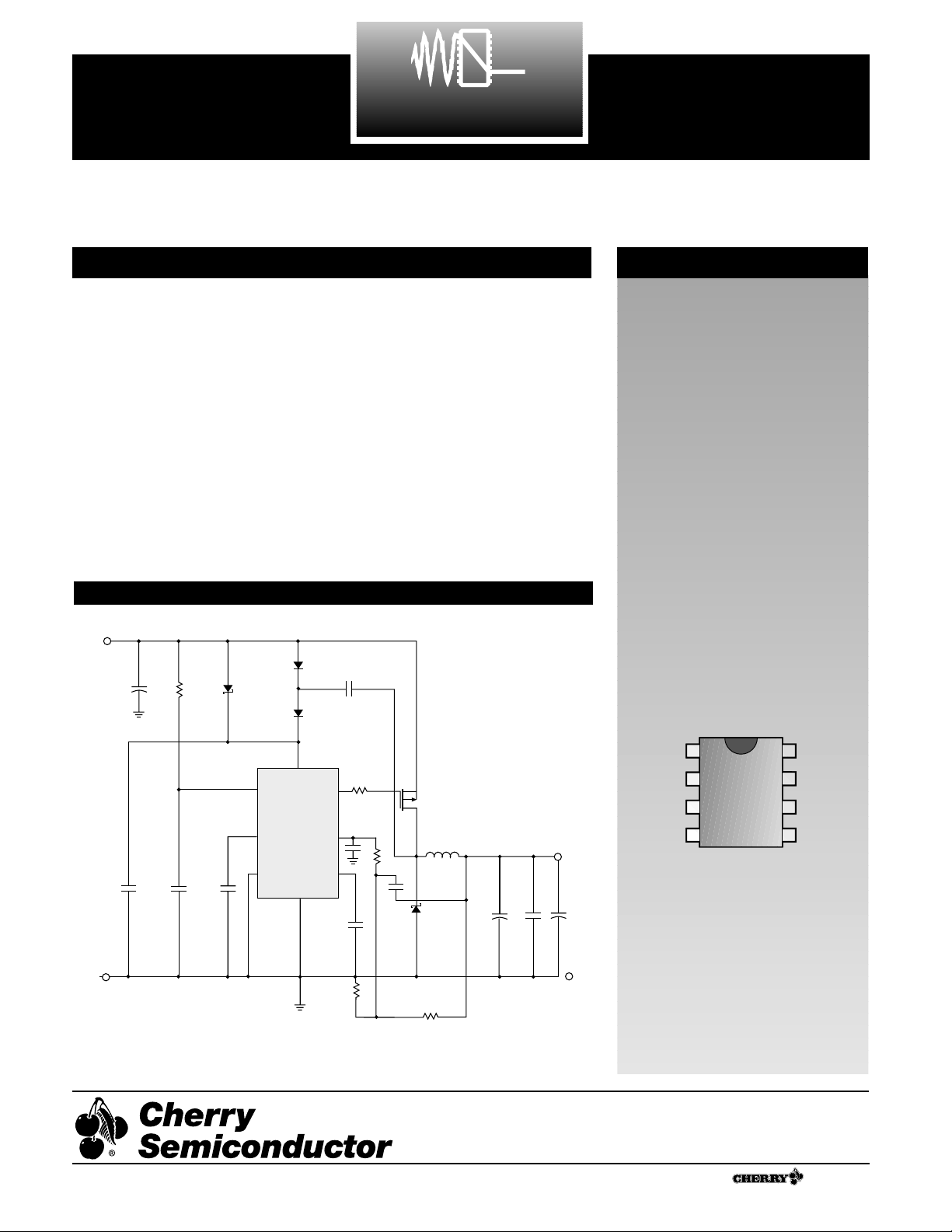
Typical Application Diagram
V
GATE
PGnd
C
OSC
Gnd
V
C
CS
V
CC
V
FB
8 Lead SO Narrow & PDIP
A Company
®
Rev. 2/13/98
Cherry Semiconductor Corporation
2000 South County Trail, East Greenwich, RI 02818
Tel: (401)885-3600 Fax: (401)885-5786
Email: info@cherry-semi.com
Web Site: www.cherry-semi.com
3.3V
IN
100µF
C
1µF
C
IN
R
C
10Ω
C
100µF
3
2
D
2
1N4148
1N4148
V
CC
C
OSC
Gnd
D
3
CS51033
PGnd
1N5818
C
OSC
150pF
D
4
C
1
0.1µF
R
V
FB
CS
0.1µF
CS
10Ω
0.01µF
G
IRF 7404
4.7µH
100
.1µF
D
1
1N5821
C
100µF
V
U1
C
V
GATE
1.5V
OUT
@3Amp
C
4
0
0.1µF
100µF
1
Gnd
NOTE: Capacitors C
caps used for noise reduction.
, C3 and C4 are low ESR tantalum
2
1.5k
R
A
300
R
B
Gnd
Page 2

Power Supply Voltage, VCC..........................................................................................................................................................5V
Driver Supply Voltage, V
C
..........................................................................................................................................................20V
Driver Output Voltage, V
GATE
...................................................................................................................................................20V
C
OSC
, CS, VFB(Logic Pins) ............................................................................................................................................................5V
Peak Output Current................................................................................................................................................................. 1.0A
Steady State Output Current ................................................................................................................................................200mA
Operating Junction Temperature, TJ..................................................................................................................................... 150°C
Storage Temperature Range, TS...................................................................................................................................-65 to 150°C
ESD (Human Body Model).........................................................................................................................................................2kV
Lead Temperature Soldering
Wave Solder (through hole styles only) .....................................................................................10 sec. max, 260°C peak
Reflow (SMD styles only) ......................................................................................60 sec. max above 183°C, 230°C peak
PARAMETER TEST CONDITIONS MIN TYP MAX UNIT
2
CS51033
Absolute Maximum Ratings
Electrical Characteristics: Specifications apply for 3.135 ≤ VCC≤ 3.465V, 3V ≤ VC≤ 16V,
-40°C ≤ TA≤ 125°C, -40°C ≤ TJ≤ 125°C, unless otherwise specified.
■ Oscillator V
FB
= 1.2V
Frequency C
OSC
= 470pF 160 200 240 kHz
Charge Current 1.4V < V
COSC
< 2V 110 µA
Discharge Current 2.7V > V
COSC
> 2V 660 µA
Maximum Duty Cycle 1 – (t
OFF/tON
) 80.0 83.3 %
■ Short Circuit Timer V
FB
= 1.0V; CS = 0.1µF; V
COSC
= 2V
Charge Current 1V < V
CS
< 2V 175 264 325 µA
Fast Discharge Current 2.55V > V
CS
> 2.4V 40 66 80 µA
Slow Discharge Current 2.4V > V
CS
> 1.5V 4 6 10 µA
Start Fault Inhibit Time 0.70 0.85 1.40 ms
Valid Fault Time 2.6V > V
CS
> 2.4V 0.2 0.3 0.45 ms
GATE Inhibit Time 2.4V > V
CS
> 1.5V 9 15 23 ms
Duty Cycle 2.5 3.1 4.6 %
■ CS Comparator V
FB
= 1V
Fault Enable CS Voltage 2.5 V
Max. CS Voltage VFB= 1.5V 2.6 V
Fault Detect Voltage VCSwhen GATE goes high 2.4 V
Fault Inhibit Voltage Minimum V
CS
1.5 V
Hold Off Release Voltage V
FB
= 0V 0.4 0.7 1.0 V
Regulator Threshold V
CS
= 1.5V 0.725 0.866 1.035 V
Voltage Clamp
■ V
FB
Comparator V
COSC
= VCS= 2V
Regulator Threshold Voltage TJ= 25°C (Note 1) 1.225 1.250 1.275 V
TJ= -40 to 125°C 1.210 1.250 1.290 V
Fault Threshold Voltage TJ= 25°C (Note 1) 1.12 1.15 1.17 V
TJ= -40 to 125°C 1.10 1.15 1.19 V
Threshold Line Regulation 3.135V ≤ VCC≤ 3.465 6 15 mV
Input Bias Current VFB= 0V 1 4 µA
Voltage Tracking (Regulator Threshold Voltage - 70 100 120 mV
Fault Threshold Voltage)
Input Hysteresis Voltage 4 20 mV
Page 3

PARAMETER TEST CONDITIONS MIN TYP MAX UNIT
CS51033
3
Package Pin Description
PACKAGE PIN # PIN SYMBOL FUNCTION
Electrical Characteristics: Specifications apply for 3.135 ≤ VCC≤ 3.465V, 3V ≤ VC≤ 16V,
-40°C ≤ TJ≤ 125°C, unless otherwise specified.
8L SO Narrow & PDIP
1V
GATE
Driver pin to gate of external PFET.
2 PGnd Output power stage ground connection.
3C
OSC
Oscillator frequency programming capacitor.
4 Gnd Logic ground.
5V
FB
Feedback voltage input.
6V
CC
Logic supply voltage.
7 CS Soft start and fault timing capacitor.
8V
C
Driver supply voltage.
■ Power Stage V
C
= 10V; VFB= 1.2V
GATE DC Low Saturation V
COSC
= 1V; 200mA Sink 1.2 1.5 V
Voltage
GATE DC High Saturation V
COSC
= 2.7V; 200mA Source; VC= V
GATE
1.5 2.1 V
Voltage
Rise Time C
GATE
= 1nF; 1.5V < V
GATE
< 9V 25 60 ns
Fall Time C
GATE
= 1nF; 9V > V
GATE
> 1.5V 25 60 ns
■ Current Drain
I
CC
3.135V < VCC< 3.465V, Gate switching 3.5 6.0 mA
I
C
3V < VC< 16V, Gate non-switching 2.7 4.0 mA
Note1: Guaranteed by design not 100% tested in production.
Page 4

CS51033
4
Block Diagram
Control Scheme
The CS51033 monitors the output voltage to determine
when to turn on the PFET. If VFBfalls below the internal reference voltage of 1.25V during the oscillator’s charge cycle,
the PFET is turned on and remains on for the duration of the
charge time. The PFET gets turned off and remains off during the oscillator’s discharge cycle time with the maximum
duty cycle to 80%. It requires 7mV typical, and 20mV maximum ripple on the VFBpin is required to operate. This
method of control does not require any loop stability compensation.
Startup
The CS51033 has an externally programmable soft start feature that allows the output voltage to come up slowly, preventing voltage overshoot on the output.
At startup, the voltage on all pins is zero. As V
CC
rises, the
VCvoltage along with the internal resistor RGkeeps the
PFET off. As VCCand VCcontinue to rise, the oscillator
capacitor (C
OSC
) and the Soft start/Fault Timing capacitor
(CS) charges via internal current sources. C
OSC
gets charged
by the current source IC and CS gets charged by the I
T
source combination described by:
I
CS
= IT -
(
+
)
The internal Holdoff Comparator ensures that the external
PFET is off until VCS> 0.7V preventing the GATE flip-flop
(F2) from being set. This allows the oscillator to reach its
operating frequency before enabling the drive output. Soft
start is obtained by clamping the V
FB
comparator’s (A6) ref-
erence input to approximately 1/2 of the voltage at the CS
pin during startup, permitting the control loop and the out-
put voltage to slowly increase. Once the CS pin charges
above the Holdoff Comparator trip point of 0.7V, the low
I
T
5
I
T
55
Theory of Operation
Circuit Description
Figure 1: Block Diagram for CS51033
V
RG
C
V
GATE
PGnd
V
FB
Gnd
V
CC
I
C
C
OSC
7I
C
1.5V
V
CC
V
CC
G3
I
T
CS
55
I
T
I
T
5
2.4V
Oscillator
Comparator
A1
2.5V
CS
Comparator
A2
2.5V1.5V
A3
+
G1
G2
G4
G5
Slow Discharge
Comparator
V
GATE
Flip-Flop
Q
R
F2
S
Q
0.7V
+
Hold
Off
Comp
-
-
Fault
Comp
1.15V
+
R
Q
F1
S
Q
Slow Discharge
Flip-Flop
A6
-
+
+
V
FB
Comparator
1.25V
CS Charge
Sense
Comparator
A4
-
2.3V
Page 5

CS51033
5
Circuit Description: continued
Applications Information
Specifications
V
IN
= 3.3V +/- 10% (i.e. 3.63V max., 2.97V min.)
V
OUT
= 1.5V +/- 2%
I
OUT
= 0.3A to 3A
Output ripple voltage < 33mV.
FSW= 200kHz.
1) Duty Cycle Estimates
Since the maximum duty cycle, D, of the CS51033 is limited
to 80% min. it is best to estimate the duty cycle for the various input conditions to see that the design will work over
the complete operating range.
The duty cycle for a buck regulator operating in a continuous conduction mode is given by:
D =
Where V
SAT
is Rdson × I
OUT
Max.
In this case we can assume that VD = 0.6V and V
SAT
= 0.6V
so the equation reduces to:
V
OUT
+ V
D
V
IN - VSAT
Designing a Power Supply with the CS51033
feedback to the VFBComparator sets the GATE flip-flop dur-
ing C
OSC
’s charge cycle. Once the GATE flip-flop is set,
V
GATE
goes low and turns on the PFET. When VCSexceeds
2.4V, the CS charge sense comparator (A4) sets the VFBcomparator reference to 1.25V completing the startup cycle.
Lossless Short Circuit Protection
The CS51033 has “Lossless” short circuit protection since
there is no current sense resistor required. When the voltage
at the CS pin (the fault timing capacitor voltage ) reaches
2.5V, the fault timing circuitry is enabled. During normal
operation the CS voltage is 2.6V. During a short circuit condition or a transient condition, the output voltage moves
lower and the voltage at VFBdrops. If VFBdrops below
1.15V, the output of the fault comparator goes high and the
CS51033 goes into a fast discharge mode. The fault timing
capacitor, CS, discharges to 2.4V. If the VFBvoltage is still
below 1.15V when the CS pin reaches 2.4V, a valid fault condition has been detected. The slow discharge comparator
output goes high and enables gate G5 which sets the slow
discharge flip flop. The Vgate flip flop resets and the output
switch is turned off. The fault timing capacitor is slowly discharged to 1.5V. The CS51033 then enters a normal startup
routine. If the fault is still present when the fault timing
capacitor voltage reaches 2.5V, the fast and slow discharge
cycles repeat as shown in figure 2.
If the VFBvoltage is above 1.15V when CS reaches 2.4V a
fault condition is not detected, normal operation resumes
and CS charges back to 2.6V. This reduces the chance of
erroneously detecting a load transient as a fault condition.
Figure 2. Voltage on start capacitor (VGS), the gate (V
GATE
), and in the
feedback loop (V
FB
), during startup, normal and fault conditions.
Buck Regulator Operation
Figure 3. Buck regulator block diagram.
A block diagram of a typical buck regulator is shown in
Figure 3. If we assume that the output transistor is initially
off, and the system is in discontinuous operation, the inductor current I
L
is zero and the output voltage is at its nominal
value. The current drawn by the load is supplied by the output capacitor CO. When the voltage across COdrops below
the threshold established by the feedback resistors R1 and
R2 and the reference voltage V
REF
, the power transistor Q1
switches on and current flows through the inductor to the
output. The inductor current rises at a rate determined by
(VIN-V
OUT
)/Load. The duty cycle (or “on” time) for the
CS51033 is limited to 80%. If the output voltage remains
higher than nominal during the entire C
OSC
charge time, the
Q1 does not turn on, skipping the pulse.
CHARGE PUMP CIRCUIT
(Refer to the CS51033 Application Diagram)
An external charge pump circuit is necessary when the input
voltage is below 5V to ensure that there is sufficient gate
drive voltage for the external FET. When V
IN
is applied,
capacitors C1 and C2 will be charged to a diodes drop below
V
IN
via diodes D2 and D4, respectively. When the PFET
turns on, its drain voltage will be approximately equal to
VIN. Since the voltage across C1 can not change instantaneously, D2 is reverse biased and the anode voltage rises to
approximately 2*3.3V-VD2. C1 transfers some of its stored
charge C2 via D3. After several cycles there is sufficient gate
drive voltage.
Control
Feedback
V
IN
L
D
1
R
1
R
2
R
LOAD
C
O
Q1
C
IN
2.5V
0V
FAULT
NORMAL OPERATION
START
T
START td1
td2
t
FAULTtRESTARTtFAULT
S2
S2
S2
S3
S3
S3
S3
S1
S1
S1
2.6V
2.4V
1.5V
0V
1.25V
1.15V
V
CS
V
GATE
V
FB
Page 6

CS51033
6
Applications Information: continued
D =
From this, the maximum duty cycle D
MAX
is 53%, this
occurs when V
IN
is at its minimum while the minimum
duty cycle D
MIN
is 0.35%.
2) Switching Frequency and on and off time calculations.
F
SW
= 200KHz. The switching frequency is determined by
C
OSC
, whose value is determined by :
C
OSC
=
95
≅
470pF
F
sw
×
(
1-
()
-
()
2
)
T = = 5µs
T
ON(MAX) =
5µs × 0.53 = 2.65µs
T
ON(MIN) =
5µs × 0.35 = 1.75µs
T
OFF(MAX) =
5µs − 0.7µs = 4.3µs
3) Inductor selection
Pick the inductor value to maintain continuous mode operation down to 0.3 Amps.
The ripple current ∆I = 2 × I
OUT(MIN)
= 2 × 0.3A = 0.6A.
L
MIN
==≅ 15µH
The CS51033 will operate with almost any value of inductor.
With larger inductors the ripple current is reduced and the
regulator will remain in a continuous conduction mode for
lower values of load current. A smaller inductor will result
in larger ripple current. The core must not saturate with the
maximum expected current, here given by:
I
MAX
= = 3A + 0.6A/2 = 3.3A
4) Output Capacitor
The output capacitor limits the output ripple voltage. The
CS51033 needs a maximum of 15mV of output ripple for the
feedback comparator to change state. If we assume that all
the inductor ripple current flows through the output capacitor and that it is an ideal capacitor (i.e. zero ESR), the minimum capacitance needed to limit the output ripple to 50mV
peak to peak is given by:
C
O =
=
≅ 11.4µF
The minimum ESR needed to limit the output voltage ripple
to 50mV peak to peak is:
ESR = = = 55mΩ
The output capacitor should be chosen so that its ESR is at
least half of the calculated value and the capacitance is at
least ten times the calculated value. It is often advisable to
use several capacitors in parallel to reduce the ESR.
Low impedance aluminum electrolytic, tantalum or organic
semiconductor capacitors are a good choice for an output
capacitor. Low impedance aluminum are the cheapest but
are not available in surface mount at present. Solid tantalum
chip capacitors are available from a number of suppliers
and offer the best choice for surface mount applications. The
capacitor working voltage should be greater than the output
voltage in all cases.
5) V
FB
Divider
V
OUT
= 1.25V
()
= 1.25V
(
+1
)
The input bias current to the comparator is 4µA. The resistor
divider current should be considerably higher than this to
ensure that there is sufficient bias current. If we choose the
divider current to be at least 250 times the bias current this
gives a divider current of 1mA and simplifies the calculations.
= R1+R2 = 1.5KΩ
Let R2 = 1K
Rearranging the divider equation gives:
R1 = R2
(
-1 ) = 1KΩ
()
= 200Ω
6) Divider bypass capacitor Crr
Since the feedback resistors divide the output voltage by a
factor of 4, i.e. 5V/1.25V= 4 it follows that the output ripple
is also divided by four. This would require that the output
ripple be at least 60mV (4 × 15mV) to trip the feedback compactor. We use a capacitor Crr to act as an ac short so that
the output ripple is not attenuated by the divider network.
The ripple voltage frequency is equal to the switching frequency so we choose Crr so that:
XC=
is negligible at the switching frequency.
In this case F
SW
is 200kHz if we allow XC = 3Ω then:
C = ≅ 0.265µF
7) Soft start and Fault timing capacitor C
S
.
CSperforms several important functions. First it provides a
dead time for load transients so that the IC does not enter a
fault mode every time the load changes abruptly. Secondly
it disables the fault circuitry during startup, it also provides
soft start by clamping the reference voltage during startup
1
2πf3
1
2πfC
1.5V
1.25
V
OUT
1.25
1.5V
1mA
R1
R2
R1 + R2
R2
50 × 10
-3
0.6A
∆V
∆I
0.6A
8 × (200 × 10
3
Hz) × (33 × 10-3V)
∆I
8 × F
SW
× ∆V
I
OUT
+ ∆I
2
2.1V × 4.3µs
0.6A
V
OUT
+ VD× Τ
OFF(MAX)
∆I
1
F
SW
30 × 10
3
F
SW
F
SW
3 × 10
6
V
OUT
V
IN
Page 7

CS51033
7
to rise slowly and finally it controls the Hiccup short circuit
protection circuitry. This function reduces the PFET's duty
cycle to 2% of the CSperiod.
The most important consideration in calculating CSis that
it’s voltage does not reach 2.5V (the voltage at which the
fault detect circuitry is enabled) before V
FB
reaches 1.15V
otherwise the power supply will never start.
If the V
FB
pin reaches 1.15V the fault timing comparator will
discharge CSand the supply will not start. For the VFBvoltage to reach 1.15V the output voltage must be at least 4 ×
1.15 = 4.6V.
If we choose an arbitrary startup time of 200µs we calculate
the value of CSfrom:
T =
C
S(min)
= = 0.02µF
Use 0.1µf.
The fault time out time is the sum of the slow discharge
time the fast discharge time and the recharge time and is
obviously dominated by the slow discharge time.
The first parameter is the slow discharge time, it is the time
for the C
S
capacitor to discharge from 2.4V to 1.5V and is
given by:
T
SLOWDISCHARGE
=
Where I
DISCHARGE
is 6µA typical.
T
SLOWDISCHARGE
= CS× 1.5V × 10
5
The fast discharge time occurs when a fault is first detected.
The CScapacitor is discharged from 2.5V to 2.4V.
T
FASTDISCHARGE
=
Where I
FASTDISCHARGE
is 66µA typical.
T
FASTDISCHARGE
= CS× 1515
The recharge time is the time for CSto charge from 1.5V to
2.5V.
T
CHARGE
=
Where I
CHARGE
is 264µA typical.
T
CHARGE
= CS× 3787
The fault time out time is given by:
T
FAULT
= CS× (3787 + 1515 + 1.5 × 10⁵)
T
FAULT
= CS× 1.55 × 10
5
For this circuit
T
FAULT
= 0.1 × 10
-6
× 1.55 × 105 = 0.0155
A larger value of CSwill increase the fault time out time but
will also increase the soft start time.
8) Input Capacitor.
The input capacitor reduces the peak currents drawn from
the input supply and reduces the noise and ripple voltage
on the VCCand VCpins. This capacitor must also ensure
that the VCCremains above the UVLO voltage in the event
of an output short circuit. C
IN
should be a low ESR capacitor
of at least 100µf. A ceramic surface mount capacitor should
also be connected between VCCand ground to prevent
spikes.
9) MOSFET Selection
The CS51033 drive a P-channel MOSFET. The V
GATE
pin
swings from Gnd to VC. The type of PFET used depends on
the operating conditions but for input voltages below 7V a
logic level FET should be used.
Choose a PFET with a continuous drain current (Id) rating
greater than the maximum output current. R
DS(on)
should be
less than
R
DS
< = 167mΩ
The Gate-to-Source voltage VGS and the Drain-to Source
Breakdown Voltage should be chosen based on the input
supply voltage.
The power dissipation due to the conduction losses is given
by:
PD =
OUT
2
× R
DS(on)
× D
The power dissipation due to the switching losses is given
by:
PD = 0.5 × V
IN
× I
OUT
× (T
Rr+ TF
) × F
SW
Where tr =Rise Time and tf= Fall Time.
10) Diode Selection.
The flyback or catch diode should be a Schottky diode
because of it’s fast switching ability and low forward voltage drop. The current rating must be at least equal to the
maximum output current. The breakdown voltage should
be at least 20V for this 12V application.
The diode power dissipation is given by:
PD = I
OUT
× VD × (1-D
MIN
)
0.6V
I
OUT(max)
CS× (2.5V-1.5V)
Ι
CHARGE
CS× (2.5V - 2.4V)
Ι
FASTDISCHARGE
CS× (2.4V-1.5V)
Ι
DISCHARGE
200µs × 264µA
2.5V
CS× 2.5V
I
CHARGE
Applications Information: continued
Page 8

8
CS51033
8
© 1999 Cherry Semiconductor Corporation
Rev. 2/13/98
Ordering Information
Part Number Description
CS51033YD8 8L SO Narrow
CS51033YDR8 8L SO Narrow (tape & reel)
CS51033YN8 8L PDIP
Cherry Semiconductor Corporation reserves the right to
make changes to the specifications without notice. Please
contact Cherry Semiconductor Corporation for the latest
available information.
Package Specification
Thermal Data 8L SO Narrow 8L PDIP
R
ΘJC
typ 45 52 ˚C/W
R
ΘJA
typ 165 100 ˚C/W
D
Lead Count Metric English
Max Min Max Min
8L SO Narrow 5.00 4.80 .197 .189
8L PDIP 10.16 9.02 .400 .355
PACKAGE DIMENSIONS IN mm (INCHES)
PACKAGE THERMAL DATA
Surface Mount Narrow Body (D); 150 mil wide
Plastic DIP (N); 300 mil wide
0.39 (.015)
MIN.
2.54 (.100) BSC
1.77 (.070)
1.14 (.045)
D
Some 8 and 16 lead
packages may have
1/2 lead at the end
of the package.
All specs are the same.
.203 (.008)
.356 (.014)
REF: JEDEC MS-001
3.68 (.145)
2.92 (.115)
8.26 (.325)
7.62 (.300)
7.11 (.280)
6.10 (.240)
.356 (.014)
.558 (.022)
1.27 (.050) BSC
0.51 (.020)
0.33 (.013)
6.20 (.244)
5.80 (.228)
4.00 (.157)
3.80 (.150)
1.57 (.062)
1.37 (.054)
D
0.25 (0.10)
0.10 (.004)
1.75 (.069) MAX
1.27 (.050)
0.40 (.016)
REF: JEDEC MS-012
0.25 (.010)
0.19 (.008)
 Loading...