

Datasheet CS51022ED16, CS51021EDR16, CS51021ED16, CS51024EDR16, CS51024ED16 Datasheet (Cherry Semiconductor)
...Page 1
The CS51021/22/23/24 Fixed
Frequency PWM Current Mode
Controller family provides all necessary features required for AC-DC or
DC-DC primary side control.
Several features are included eliminating the additional components
needed to implement them externally. In addition to low start-up current (75µA) and high frequency
operation capability, the CS51021/
22/23/24 family includes overvoltage and undervoltage monitoring,
externally programmable dual
threshold overcurrent protection,
current sense leading edge blanking, current slope compensation,
accurate duty cycle control and an
externally available 5V reference.
The CS51021 and CS51023 feature
bidirectional synchronization capability, while the CS51022 and
CS51024 offer a sleep mode with
100µA maximum IC current consumption. The CS51021/22/23/24
family is available in a 16 lead narrow body SO package.
1
Features
■ 75µA Max. Startup Current
■ Fixed Frequency Current
Mode Control
■ 1MHz Switching Frequency
■ Undervoltage Protection
Monitor
■ Overvoltage Protection
Monitor with
Programmable Hysteresis
■ Programmable Dual
Threshold Overcurrent
Protection with Delayed
Restart
■ Programmable Soft Start
■ Accurate Maximum Duty
Cycle Limit
■ Programmable Slope
Compensation
■ Leading Edge Current
Sense Blanking
■ 1A Sink/Source Gate Drive
■ Bidirectional Synchronization
(CS51021/23)
■ 50ns PWM Propagation
Delay
■ 100µA Max Sleep Current
(CS51022/24)
Package Options
CS51021/22/23/24
Enhanced Current Mode
PWM Controller
CS51021/CS51023
CS51022/CS51024
Description
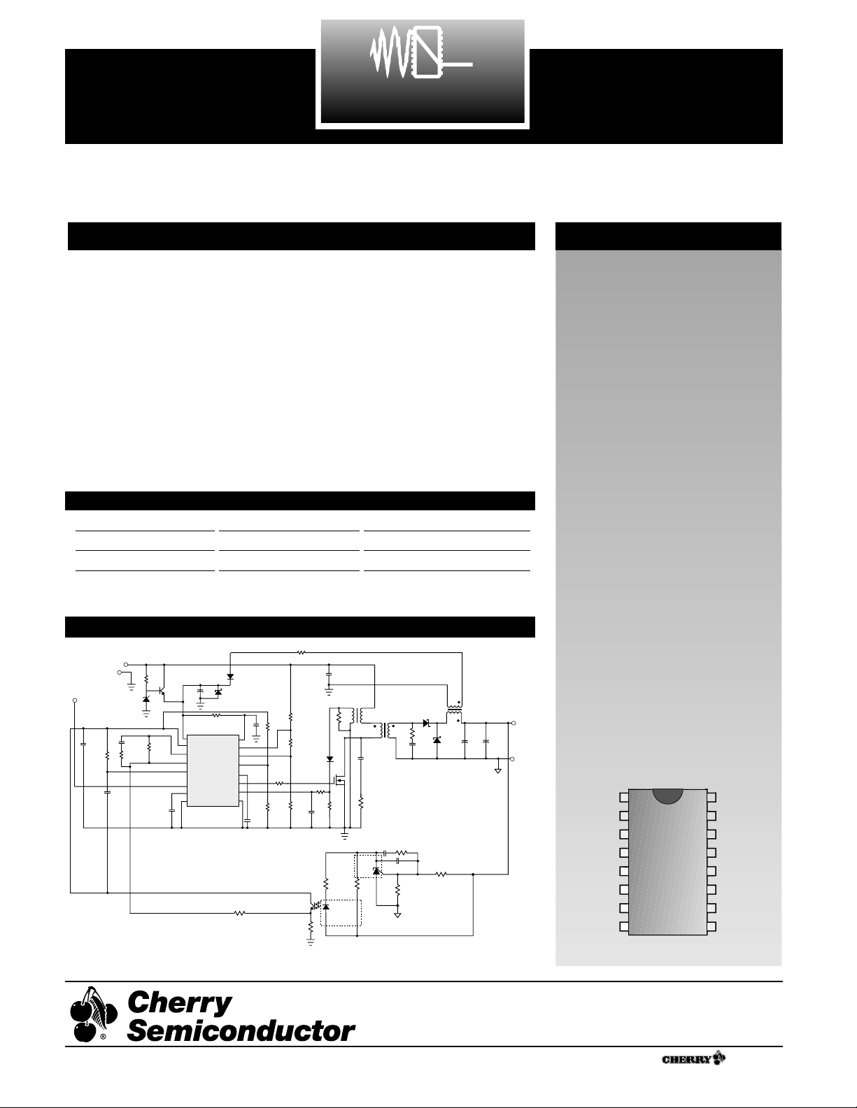
Typical Application Diagram
SS
V
REF
OV
SLEEP
or SYNC
V
FB
RTC
T
V
CC
SLOPE
I
SET
PGnd
I
SENSE
COMP
LGnd
UV
V
C
GATE
16 Lead SO Narrow
Device Sleep/Synch VCCStart/Stop
CS51021 Synch 8.25V/7.7V
CS51022 Sleep 8.25V/7.7V
CS51023 Synch 13V/7.7V
CS51024 Sleep 13V/7.7V
A Company
®
36-72V to 5V, 5A DC-DC Convertor
Rev. 2/22/99
Cherry Semiconductor Corporation
2000 South County Trail, East Greenwich, RI 02818
Tel: (401)885-3600 Fax: (401)885-5786
Email: info@cherry-semi.com
Web Site: www.cherry-semi.com
Consult factory for other package options.
V
(36V to 72V)
IN
PGND
SYNC/SLEEP
0.01µF
10K
330pF
51k
11V
4700pF
51K
0.01µF
BAS21
18V
22µF
FZT688
22K
V
C
V
REF
COMP
V
FB
RTC
SYNC/
SLEEP
C
SS
LGnd
10
T
SLOPE
CS51021/51022
U1
GATE
I
SENSE
PGnd
V
CC
UV
OV
I
SET
100
1µF
100
100p
100:1
4:1
10K
100pF
10
62
0.1µF
470pF
24.3K
1%
6.98k,
1%
200K,1%
2.49K,1%
BA521
IRF6345
10
6.98k,
1%
MBRB2060CT
10
680pF
2:5
100µF
100µF
V
OUT
(5V/5A)
SGND
1
10K
0.1µF
5.1K
TL431
1000pF
180
1K
MOC81025
1K
2K, 1%
2K,1%
Page 2
Power Supply Voltage, VCC............................................................................................................................................-0.3V, 20V
Driver Supply Voltage, V
C
..............................................................................................................................................-0.3V, 20V
SYNC, SLEEP, R
TCT
, SOFT START, VFB, SLOPE, I
SENSE
, UV, OV, I
SET
(Logic Pins).......................................-0.25V to V
REF
Peak GATE Output Current.........................................................................................................................................................1A
Steady State Output Current..................................................................................................................................................± 0.2A
Operating Junction Temperature, TJ..................................................................................................................................... 150°C
Storage Temperature Range, T
S
...................................................................................................................................-65 to 150°C
ESD (Human Body Model).........................................................................................................................................................2kV
Lead Temperature Soldering: Reflow (SMD styles only).............................................60 sec. max above 183°C, 230°C peak
PARAMETER TEST CONDITIONS MIN TYP MAX UNIT
2
CS51021/22/23/24
Absolute Maximum Ratings
■ Under Voltage Lockout
START Threshold (CS51021/22) 7.95 8.25 8.8 V
START Threshold (CS51023/24) 12.4 13 13.4 V
STOP Threshold 7.4 7.7 8.2 V
Hysteresis (CS51021/22) 0.50 0.75 1.00 V
Hysteresis (CS51023/24) 4 5 6 V
I
CC
@ Startup (CS51021/22) V
CC
< UV
START
Threshold 40 75 µA
I
CC
@ Startup (CS51023/24) V
CC
< UV
START
Threshold 45 75 µA
I
CC
Operating (CS51021/23) 7 9 mA
I
CC
Operating (CS51022/24) 6 8 mA
I
C
Operating Includes 1nF Load 7 12 mA
■ Voltage Reference
Initial Accuracy T
A
= 25C, I
REF
= 2mA, VCC= 14V (Note1) 4.95 5 5.05 V
Total Accuracy 1mA<I
REF
<10mA 4.9 5 5.15 V
Line Regulation 8.2V < V
CC
< 18V, I
REF
= 2mA 6 20 mV
Load Regulation 1mA < I
REF
< 10mA 6 15 mV
NOISE Voltage (Note 1) 50 uV
OP Life Shift T=1000 Hours (Note 1) 4 20 mV
FAULT Voltage Force V
REF
.92 × V
REF
.95 × V
REF
.97 × V
REF
V
OK Voltage Force V
REF
.94 × V
REF
.96 × V
REF
.98 × V
REF
V
OK Hysteresis Force V
REF
50 105 160 mV
Current Limit Force V
REF
-20 mA
■ Error Amplifier
Initial Accuracy T
A
=25°C, I
REF
= 2mA, V
CC
= 14V, 2.465 2.515 2.565 V
V
FB
= COMP (Note 1)
Reference Voltage V
FB
= COMP 2.440 2.515 2.590 V
V
FB
Leakage Current V
FB
= 0V -0.2 -2 µA
Open Loop Gain 1.4V < COMP < 4V (Note 1) 60 90 dB
Unity Gain Bandwidth (Note 1) 1.5 2.5 MHz
COMP Sink Current COMP = 1.5V, V
FB
= 2.7V 2 6 mA
COMP Source Current COMP = 1.5V, V
FB
= 2.3V -0.2 -0.5 mA
Electrical Characteristics: Unless otherwise stated, specifications apply for -40°C < TA< 85°C, -40°C < TJ< 150°C,
3V < V
C
< 20V, 8.2V < VCC< 20V, RT= 12kΩ, CT= 390pF.
Page 3
3
CS51021/22/23/24
PARAMETER TEST CONDITIONS MIN TYP MAX UNIT
Electrical Characteristics: -40°C < TA< 85°C, -40°C < TJ< 150°C, 3V < VC< 20V, 8.2V < VCC< 20V,
R
T
= 12kΩ, CT= 390pF, unless otherwise stated
■ Error Amplifier continued
COMP High Voltage V
FB
= 2.3V 4.35 4.8 5 V
COMP Low Voltage V
FB
= 2.7V 0.4 0.8 1.2 V
PS Ripple Rejection FREQ = 120Hz (Note 1) 60 85 dB
SS Clamp, V
COMP
VSS=2.5V, V
FB
= 0V, I
SET
= 2V 2.4 2.5 2.6 V
I
LIM(SET)
Clamp (Note 1) 0.95 1 1.15 V
■ Oscillator
Accuracy R
T
= 12k, CT= 390pF 230 255 280 kHz
Voltage Stability Delta Frequency 8.2V < V
CC
< 20V 2 3 %
Temperature Stability T
MIN
< TA < T
MAX
(Note1) 8 %
Min Charge & Discharge Time (Note1) 0.333 µs
Duty Cycle Accuracy R
T
= 12k, CT= 390pF 70 77 83 %
Peak Voltage (Note 1) 3 V
Valley Voltage (Note 1) 1.5 V
Valley Clamp Voltage 10k Resistor to ground on R
TCT
1.2 1.4 1.6 V
Discharge Current 0.8 1 1.2 mA
Discharge Current T
A
=25°C (Note 1) 0.925 1 1.075 mA
■ Synchronization (CS51021/23)
Input Threshold 1.0 1.5 2.7 V
Output Pulsewidth 160 260 360 ns
Output High Voltage I
SYNC
= 100µA 3.5 4.3 4.8 V
Input Resistance (Note 1) 35 70 140 kΩ
Drive Delay SYNC to GATE RESET 80 120 150 ns
Output Drive Current 1k Load 1.25 2 3.5 mA
■ SLEEP (CS51022/24)
SLEEP Input Threshold Active High 1.0 1.5 2.7 V
SLEEP Input Current V
SLEEP
= 4V 11 25 46 µA
I
CC
@ SLEEP V
CC
≤ 15V 50 100 µA
■ GATE Driver
HIGH Voltage Measure V
C
-GATE, VC = 10V, 150mA Load 1.5 2.2 V
LOW Voltage Measure GATE-PGnd, 150mA SINK 1.2 1.5 V
HIGH Voltage Clamp V
C
= 20V, 1nF 11 13.5 16 V
LOW Voltage Clamp Measured at 10mA Output Current 0.6 0.8 V
Peak Current V
C
= 20V, 1nF (Note 1) 1 A
UVL Leakage V
C
= 20V, measured at 0V -1 -50 µA
RISE Time Load = 1nF, 1V < GATE < 9V, 60 100 ns
V
C
= 20V, TA= 25˚C
FALL Time Load = 1nF, 9V > GATE > 1V, V
C
= 20V 15 40 ns
Page 4

PARAMETER TEST CONDITIONS MIN TYP MAX UNIT
CS51021/22/23/24
4
Electrical Characteristics: Unless otherwise stated, specifications apply for -40°C < TA< 85°C, -40°C < TJ< 150°C,
3V < V
C
< 20V, 8.2V < VCC< 20V, RT= 12kΩ, CT= 390pF.
Package Pin Description
PACKAGE PIN # PIN SYMBOL FUNCTION
■ SLOPE Compensation
Charge Current SLOPE = 2V -63 -53 -43 µA
COMP Gain Fraction of slope voltage added 0.095 0.100 0.105 V/V
to I
SENSE
(Note 1)
Discharge Voltage SYNC = 0V 0.1 0.2 V
■ Current Sense
OFFSET Voltage (Note 1) 0.09 0.10 0.11 V
Blanking Time 55 160 ns
Blanking Disable Voltage Adjust V
FB
1.8 2 2.2 V
Second Current Threshold Gain 1.21 1.33 1.45 V/V
I
SENSE
Input Resistance 5 kΩ
Minimum On Time GATE High to Low 30 70 110 ns
Gain (Note 1) 0.78 0.80 0.82 V/V
■ OV & UV Voltage Monitors
OV Monitor Threshold 2.4 2.5 2.6 V
OV Hysteresis Current -10 -12.5 -15 µA
UV Monitor Threshold 1.38 1.45 1.52 V
UV Monitor Hysteresis 25 75 100 mV
■ SOFT START (SS)
Charge Current SS = 2V -70 -55 -40 µA
Discharge Current SS = 2V 250 1000 µA
Charge Voltage, V
SS
4.4 4.7 5 V
Discharge Voltage, V
SS
0.25 0.27 0.30 V
Note 1: Guaranteed by Design, not 100% tested in production.
16L PDIP & SO Narrow
1 GATE External power switch driver with 1.0A peak capability.
2I
SENSE
Current sense amplifier input.
3 SYNC Bi-directional synchronization. Locks to the highest frequency.
(CS51021/23)
3 SLEEP Active high chip disable. In sleep mode, V
REF
and GATE are
(CS51022/24) turned off.
4 SLOPE Additional slope to the current sense signal. Internal current
source charges the external capacitor.
5 UV Undervoltage protection monitor.
6 OV Overvoltage protection monitor.
Page 5

CS51021/22/23/24
5
Package Pin Description: continued
PACKAGE PIN # PIN SYMBOL FUNCTION
Figure 1: CS51021/22/23/24 Block Diagram
Block Diagram
16L PDIP & SO Narrow
7R
TCT
Timing resistor RTand capacitor CTdetermine oscillator frequency and maximum duty cycle, D
MAX
.
8I
SET
Voltage at this pin sets pulse-by-pulse overcurrent threshold, and
second threshold (1.33 times higher) with Soft Start retrigger (hic-
cup mode).
9V
FB
Feedback voltage input. Connected to the error amplifier inverting input.
10 COMP Error amplifier output. Frequency compensation network is usu-
ally connected between COMP and V
FB
pins.
11 SS Charging external capacitor restricts error amplifier output volt-
age during the start or fault conditions (hiccup).
12 LGnd Logic ground.
13 V
REF
5.0V reference voltage output.
14 V
CC
Logic supply voltage.
15 PGnd Output power stage ground connection.
16 V
C
Output power stage supply voltage.
V
LGnd
SLEEP
SYNC
R
TCT
COMP
V
SLOPE
I
SENSE
I
SET
OV
CC
REF
SS
E/A
4.3V
V
FB
Monitor
∑
+
–
Vcc_OK
0.1V
–
1.33
2.5V
D
+
200ns
2
-
+
2.5V
-
FB
V
REF
53µA
Q
2
START
+
STOP
Clamp
+
2V
–
×
0.1
×
0.8
V
12.5µA
V
REF
OSC
I
SET
Clamp
20k
D
1
10k
G
4
DISABLE
55ns
Blank
×
OV
Monitor
= 5V
V
REF
V
REF_OK
+
4.75V
G
2
Q
S
Discharge
Latch
UV
Monitor
D
55µA
4
V
REF
+
1.45V
–
F
1
G
1
D
3
PWM
Comp
SS
Monitor
V
ISense
2nd
Threshold
R
+
4.7V
–
G
3
FAULT
ZD
13.5V
V
C
GATE
1
PGnd
SS
UV
Page 6

6
CS51021/22/23/24
Circuit Description
Figure 2: Typical Waveforms
Powering the IC
The IC has two supply and two ground pins. VCand
PGnd pins provide high speed power drive for the external power switch. VCCand LGnd pins power the control
portion of the IC. The internal logic monitors the supply
voltage, VCC. During abnormal operating conditions, the
output is held low. The CS51021/22/23/24 requires only
75µA of startup current.
Voltage Feedback
The output voltage is monitored via the V
FB
pin and is
compared with the internal 2.5V reference. The error
amplifier output minus one diode drop is divided by 3
and connected to the negative input of the PWM comparator. The positive input of the PWM comparator is connected to the modified current sense signal. The oscillator
turns the external power switch on at the beginning of
each cycle. When current sense ramp voltage exceeds the
reference side of PWM comparator, the output stage latches off. It is turned on again at the beginning of the next
oscillator cycle.
Current Sense and Protection
The current is monitored at the I
SENSE
pin. The
CS51021/22/23/24 has leading edge blanking circuitry
that ignores the first 55ns of each switching period.
Blanking is disabled when V
FB
is less than 2V so that the
minimum on-time of the controller does not have an additional 55ns of delay time during fault conditions. For the
remaining portion of the switching period, the current
sense signal, combined with a fraction of the slope compensation voltage, is applied to the positive input of the
PWM comparator where it is compared with the divided
by three error amplifier output voltage. The pulse-bypulse overcurrent protection threshold is set by the voltage at the I
SET
pin. This voltage is passed through the I
SET
Clamp and appears at the non-inverting input of the PWM
comparator, limiting its dynamic range according to the
following formula:
Overcurrent Threshold= 0.8 × V
I(SENSE)
+0.1V + 0.1 V
SLOPE
where
V
I(SENSE)
is voltage at the I
SENSE
pin
and
V
SLOPE
is voltage at the SLOPE pin.
During extreme overcurrent or short circuit conditions,
the slope of the current sense signal will become much
steeper than during normal operation. Due to loop propagation delay, the sensed signal will overshoot the pulseby-pulse threshold eventually reaching the second overcurrent protection threshold which is 1.33 times higher
than the first threshold and is described by the following
equation:
2nd Threshold = 1.33 × V
I(SET)
Exceeding the second threshold will reset the Soft Start
capacitor C
SS
and reinitiate the Soft Start sequence, repeat-
ing for as long as the fault condition persists.
Soft Start
During power up, when the output filter capacitor is discharged and the output voltage is low, the voltage across
the Soft Start capacitor (VSS) controls the duty cycle. An
internal current source of 55µA charges CSS. The maximum error amplifier output voltage is clamped by the SS
Clamp. When the Soft Start capacitor voltage exceeds the
error amplifier output voltage, the feedback loop takes
over the duty cycle control. The Soft Start time can be estimated with the following formula:
tSS= 9 × 10⁴× C
SS
The Soft Start voltage, VSS, charges and discharges
between 0.25V and 4.7V.
Slope Compensation
DC-DC converters with current mode control require a
current sense signal with slope compensation to avoid
instability at duty cycles greater than 50%. Slope capacitor
C
S
is charged by an internal 53µA current source and is
discharged during the oscillator discharge time. The slope
compensation voltage is divided by 10 and is added to the
current sense voltage, V
I(SENSE)
. The signal applied to the
Theory of Operation
200ns
4.3V
T
0V
V
SLOPE
0V
0V
0V
0V
V
IN
0V
CH
IS + 0.1 SLOPE
IS
T
DIS
55ns Blanking
SYNC
R
TCT
SLOPE
IS
V
COMP
PWM COMP
GATE
V
DS
Page 7

7
input of the PWM comparator is a combination of these
two voltages. The slope compensation, , is calculated using the following formula:
= 0.1 ×
It should be noted that internal capacitance of the IC will
cause an error when determining slope compensation
capacitance C
S
. This error is typically small for large values of CS, but increases as CSbecomes small and comparable to the internal capacitance. The effect is apparent as a
reduction in charging current due to the need to charge
the internal capacitance in parallel with CS. Figure 3 shows
a typical curve indicating this decrease in available charging current.
Figure 3: The slope compensation pin charge current reduces when a
small capacitor is used.
Undervoltage (UV) and Overvoltage (OV) Monitor
Two independent comparators monitor OV and UV conditions. A string of three resistors is connected in series
between the monitored voltage (usually the input voltage)
and ground (see Figure 4). When voltage at the OV pin
exceeds 2.5V, an overvoltage condition is detected and
GATE shuts down. An internal 12.5µA current source
turns on and feeds current into the external resistor, R3,
creating a hysteresis determined by the value of this resistor (the higher the value, the greater the hysteresis). The
hysteresis voltage of the OV monitor is determined by the
following formula:
V
OV(HYST)
= 12.5µA × R
3
where R3is a resistor connected from the OV pin to ground.
When the monitored voltage is low and the UV pin is less
than 1.45V, GATE shuts down. The UV pin has fixed 75mV
hysteresis.
Both OV and UV conditions are latched until the Soft Start
capacitor is discharged. This way, every time a fault condition is detected the controller goes through the power
up sequence.
Figure 4: UV/OV Monitor Divider
To calculate the OV/UV resistor divider:
1. Solve for R3, based on OV hysteresis requirements.
R
3
= ’
where V
OV(HYST)
is the desired amount of overvoltage hys-
teresis, and V
MAX
is the input voltage at which the supply
will shut down.
2. Find the total impedance of the divider.
R
TOT
= R1+ R2+ R3=
3. Determine the value of R2from the UV threshold conditions.
R2= − R
3,
where V
MIN
is the UV voltage at which the supply will
shut down.
4. Calculate R1.
R1= R
TOT
− R2− R
3
5. The undervoltage hysteresis is given by:
V
UV(HYST)
=
Synchronization
A bi-directional synchronization is provided to synchronize several controllers. When SYNC pins are connected
together, the converters will lock to the highest switching
frequency. The fastest controller becomes the master, producing a 4.3V, 200ns pulse train. Only one, the highest frequency SYNC signal, will appear on the SYNC line.
Sleep
The sleep input is an active high input. The CS51022/51024
is placed in sleep mode when SLEEP is driven high. In
sleep mode, the controller and MOSFET are turned off.
Connect to Gnd for normal operation. The sleep mode
operates at VCC≤ 15V.
Oscillator and Duty Cycle Limit
The switching frequency is set by RTand CTconnected to
the RTCTpin. CTcharges and discharges between 3V and
1.5V.
The maximum duty cycle is set by the ratio of the on time,
tON, and the whole period, T = tON+ t
OFF
. Because the
V
MIN
× 0.075
1.45
1.45 × R
TOT
V
MIN
V
MAX
× R
3
2.5
V
OV(HYST)
× 2.5V
V
MAX
× 12.5µA
53µA
C
S
dV
SLOPE
dt
dV
SLOPE
dt
Circuit Description: continued
CS51021/22/23/24
R
V
IN
1
R
2
V
UV
R
3
V
OV
60
55
50
45
40
35
30
Charging Current (µA)
25
20
10 100 1000
Compensation Cap (pF)
Page 8

CS51021/22/23/24
8
timing capacitor’s discharge current is trimmed, the maximum duty cycle is well defined. It is determined by the
ratio between the timing resistor R
T
and the timing capacitor CT. Refer to figures 5 and 6 to select appropriate values
for RT and C
T.
f
SW
= ; T
SW
= tCH+ t
DIS
Figure 5: Frequency vs. RTfor Discrete Capacitor Values.
Figure 6: Duty Cycle vs. R
T
for Discrete Capacitor Values.
1
T
SW
Circuit Description: continued
2500
1
2000
1500
2
1000
Frequency (kHz)
3
4
500
5
8
0
10 15 20 25 30 355404550
6
7
RT (kΩ)
1. CT = 47pF
2. CT = 100pF
3. CT = 150pF
4. CT = 220pF
5. CT = 390pF
6. CT = 470pF
7. CT = 560pF
8. C
= 680pF
T
100
90
80
70
Duty Cycle (%)
60
50
40
10 15 20 25 30 355404550
5
1
6
4
3
2
RT (kΩ)
1. CT = 47pF
2. CT = 100pF
3. C
4. C
5. CT = 390pF
6. CT = 470pF
7. CT = 560pF
8. C
8
7
= 150pF
T
= 220pF
T
= 680pF
T
55
Page 9

CS51021/22/23/24
9
Part Number Description
CS51021ED16 16L SO Narrow
CS51021EDR16 16L SO Narrow (tape & reel)
CS51022ED16 16L SO Narrow
CS51022EDR16 16L SO Narrow (tape & reel)
CS51023ED16 16L SO Narrow
CS51023EDR16 16L SO Narrow (tape & reel)
CS51024ED16 16L SO Narrow
CS51024EDR16 16L SO Narrow (tape & reel)
Rev. 2/22/99
Ordering Information
Package Specification
Thermal Data 16L SO Narrow
R
ΘJC
typ 28 ˚C/W
R
ΘJA
typ 115 ˚C/W
D
Lead Count Metric English
Max Min Max Min
16L SO Narrow 10.00 9.80 .394 .386
PACKAGE DIMENSIONS IN mm (INCHES)
PACKAGE THERMAL DATA
© 1999 Cherry Semiconductor Corporation
Cherry Semiconductor Corporation reserves the
right to make changes to the specifications without
notice. Please contact Cherry Semiconductor
Corporation for the latest available information.
Surface Mount Narrow Body (D); 150 mil wide
1.27 (.050) BSC
0.51 (.020)
0.33 (.013)
6.20 (.244)
5.80 (.228)
4.00 (.157)
3.80 (.150)
1.57 (.062)
1.37 (.054)
D
0.25 (0.10)
0.10 (.004)
1.75 (.069) MAX
1.27 (.050)
0.40 (.016)
REF: JEDEC MS-012
0.25 (.010)
0.19 (.008)
 Loading...