

Page 1
1
Features
■
1.5A Peak Output
(Grounded Totem Pole)
■
8V to 75V Gate Drive Voltage
■
8V to 45V Supply Voltage
■
300ns Propagation Delay
■
1% Error Amplifier
Reference Voltage
■
Lossless Turn On and
Turn Off
■
Sleep Mode: < 100µA
■
Overcurrent Protection with
Dedicated Differential Amp
■
Synchronization to External
Clock
■
External Power Switch
Drain Voltage Monitor
Package Options
16L SO Wide
14L PDIP
CS5101
Secondary Side Post Regulator for AC/DC
and DC/DC Multiple Output Converters
SYNC
V
CC
V
REF
DGnd
V
FB
COMP
RAMP
V
C
PGnd
IS-
IS+
IS COMP
V
D
V
G
PGnd
AGnd
SYNC
V
CC
V
REF
LGnd
V
FB
COMP
RAMP
V
C
PGnd
IS-
IS+
IS COMP
V
D
V
G
CS5101
Description
The CS5101 is a bipolar monolithic
secondary side post regulator
(SSPR) which provides tight regulation of multiple output voltages in
AC-DC or DC-DC converters.
Leading edge pulse width modulation is used with the CS5101.
The CS5101 is designed to operate
over an 8V to 45V supply voltage
(VCC) range and up to a 75V drive
voltage (VC).
The CS5101 features include a totem
pole output with 1.5A peak output
current capability, externally programmable overcurrent protection,
an on chip 2% precision 5V reference, internally compensated error
amplifier, externally synchronized
switching frequency, and a power
switch drain voltage monitor. It is
available in a 14 lead plastic DIP or
a 16 lead wide body SO package.
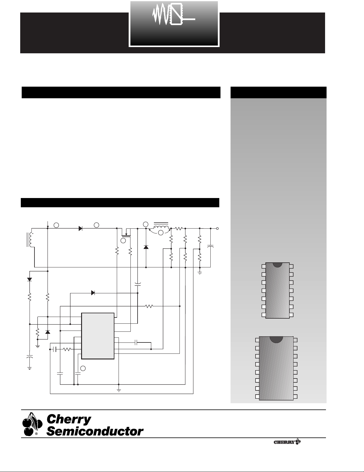
Application Diagram
Cherry Semiconductor Corporation
2000 South County Trail, East Greenwich, RI 02818
Tel: (401)885-3600 Fax: (401)885-5786
Email: info@cherry-semi.com
Web Site: www.cherry-semi.com
A Company
¨
Rev. 3/31/97
V
SY
TR
C
R1
1
C
R4
3
L1
Q1
6
R5
4
C
R6
R5
C5
+
R10
5
R8
R11
R12
R9
R14
R13
Gnd
V
OUT
+
C6
1
R1
+
R2
C
R3
R2
R4
C1
C2
C3
V
V
V
LGnd
V
COMP
RAMP
2
C
SYNC
CC
REF
FB
R
C
R3
CS5101
SSPR
PGnd
IS COMP
R7
V
D
V
C
V
G
C4
IS-
IS+
1
Page 2

2
PARAMETER TEST CONDITIONS MIN TYP MAX UNIT
CS5101
Absolute Maximum Ratings
Power Supply Voltage, VCC.....................................................................................................................................-0.3V to 45V
V
SYNC
and Output Supply Voltages, VC, VG, V
SYNC
, VD.....................................................................................-0.3V to 75V
VIS+, VIS- (VCCÐ 4V, up to 24V)..................................................................................................................................-0.3 to 24V
V
REF
, VFB, V
COMP
, V
RAMP
, V
ISCOMP
............................................................................................................................-0.3 to 10V
Operating Junction Temperature, TJ.......................................................................................................................-40 to 150¡C
Operating Temperature Range ..................................................................................................................................-40 to 85¡C
Storage Temperature Range ....................................................................................................................................-65 to 150¡C
Output Energy (capacitive load per cycle).............................................................................................................................5µJ
ESD Human Body ....................................................................................................................................................................2kV
ESD Machine Model...............................................................................................................................................................200V
Lead Temperature Soldering
Wave Solder (through hole styles only)....................................................................................10 sec. max, 260¡C peak
Reflow (SMD styles only).....................................................................................60 sec. max above 183¡C, 230¡C peak
Electrical Characteristics:
-40¡C ² TA² 85¡C; -40¡C ² TJ² 150¡C; 10V < VCC< 45V; 8V < VC<75V unless otherwise specified.
■ Error Amplifier
Input Voltage Initial Accuracy V
FB
= V
COMP
; VCC= 15V; 1.98 2.00 2.02 V
T = 25¡C (Note 1)
Input Voltage V
FB
= V
COMP
, includes line and temp 1.94 2.00 2.06 V
Input Bias Current V
FB
= 0V; IVFBflows out of pin 500 nA
Open Loop Gain 1.5V < V
COMP
< 3.0V 60 70 dB
Unity Gain Bandwidth 1.5V < V
COMP
< 3.0V; (Note 1) 0.7 1.0 MHz
Output Sink Current V
COMP
= 2.0V; VFB= 2.2V 2 8 mA
Output Source Current V
COMP
= 2.0V; VFB= 1.8V 2 6 mA
V
COMP
High VFB= 1.8V 3.3 3.5 3.7 V
V
COMP
Low VFB= 2.2V 0.85 1.0 1.15 V
PSRR 10V < V
CC
< 45V; 60 70 dB
V
FB
= V
COMP
(Note 1)
■ Voltage Reference
Output Voltage Initial Accuracy V
CC
= 15V; T = 25¡C (Note 1) 4.9 5.0 5.1 V
Output Voltage 0A < I
REF
< 8mA 4.8 5.0 5.2 V
Line Regulation 10V < V
CC
< 45V; I
REF
= 0A 10 60 mV
Load Regulation 0A < I
REF
< 8mA 20 60 mV
Current Limit V
REF
= 4.8V 10 50 mA
V
REF
_OK FAULT V V
SYNC
= 5V; V
REF
= V
LOAD
4.10 4.40 4.60 V
V
REF
_OK V V
SYNC
= 5V; V
REF
= V
LOAD
4.30 4.50 4.80 V
V
REF
_OK Hysteresis 40 100 250 mV
■ Current Sense Amplifier
IS COMP High V IS
+
= 5V; ISÐ= IS COMP 4.7 5.0 5.3 V
IS COMP Low V IS
+
= 0V; ISÐ= IS COMP 0.5 1.0 1.3 V
Source Current IS
+
= 5V; ISÐ= 0V 2.0 10 mA
Sink Current IS
-
= 5V; IS+= 0V 10 20 mA
Open Loop Gain 1.5V ² V
COMP
² 4.5V; RL= 4k½ 60 80 dB
CMRR (Note 1) 60 80 dB
PSRR 10V < V
CC
< 45V, (Note 1) 60 80 dB
Unity Gain Bandwidth 1.5V ² V
COMP
² 4.5V; RL= 4k½ (Note 1) 0.5 0.8 MHz
Page 3

3
CS5101
Electrical Characteristics: continued
PARAMETER TEST CONDITIONS MIN TYP MAX UNIT
■ Current Sense Amplifier: continued
Input Offset Voltage V
IS
+ = 2.5V; VIS- = V
ISCOMP
-8 0 8 mV
Input Bias Currents V
IS
+ = VIS- = 0V; IISflows out of pins 20 250 nA
Input Offset Current (IS
+
, IS-) -250 0 250 nA
Input Signal Voltage Range (Note 1) -0.3 V
CC
-4.0 V
■ RAMP/SYNC Generator
Ramp Source Current Initial V
SYNC
= 5V, V
RAMP
= 2.5V ; T = 25¡C 0.18 0.20 0.22 mA
Accuracy (Note 1)
Ramp Source Current V
SYNC
= 5V; V
RAMP
= 2.5V 0.16 0.20 0.24 mA
Ramp Sink Current V
SYNC
= 0V; V
RAMP
= 2.5V 1.0 4.0 mA
RAMP Peak Voltage V
SYNC
= 5V 3.3 3.5 3.7 V
RAMP Valley Voltage V
SYNC
= 0V 1.4 1.5 1.6 V
RAMP Dynamic Range V
RAMPDR
= V
RAMPPK
Ð V
RAMPVY
1.7 2.0 2.3 V
RAMP Sleep Threshold Voltage V
RAMP
@ V
REF
< 2.0V 0.3 0.6 1.0 V
SYNC Threshold V
SYNC
@ V
RAMP
> 2.5V 2.3 2.5 2.7 V
SYNC Input Bias Current V
SYNC
= 0V; I
SYNC
flows out of pin 1 20 µA
■ Output Stage
V
G
, High V
SYNC
= 5V; IVG= 200mA, VCÐ V
G
1.6 2.5 V
V
G
, Low V
SYNC
= 0V; IVG= 200mA 0.9 1.5 V
V
G
Rise Time Switch V
SYNC
High; CG= 1nF; 30 75 ns
VCC= 15V; measure 2V to 8V
V
G
Fall Time Switch V
SYNC
Low; CG= 1nF 40 100 ns
VCC= 15V; measure 8V to 2V
V
G
Resistance to Gnd Remove supplies; VG= 10V 50 100 k½
V
D
Resistance to Gnd Remove supplies; VD= 10V 500 1500 ½
■ General
I
CC
, Operating V
SYNC
= 5V 12 18 mA
I
CC
in UVL VCC= 6V 300 500 µA
I
CC
in Sleep Mode High V
RAMP
= 0V; VCC= 45V 80 200 µA
I
CC
In Sleep Mode Low V
RAMP
= 0V; VCC= 10V 20 50 µA
I
C
, Operating High V
SYNC
= 5V; V
FB
= VISÐ = 0V; 4 8 mA
VC= 75V
I
C
, Operating Low V
SYNC
= 5V; V
FB
= VISÐ = 0V; VC= 8V 3 6 mA
UVLO Start Voltage 7.4 8.0 9.2 V
UVLO Stop Voltage 6.4 7.0 8.3 V
UVLO Hysteresis 0.8 1.0 1.2 V
Leading Edge, t
DELAY
V
SYNC
= 2.5V to VG= 8V 280 ns
Trailing Edge, t
DELAY
V
SYNC
= 2.5V to VG= 2V 750 ns
Note 1: Guaranteed by design. Not 100% tested in production.
Page 4

4
CS5101
PACKAGE PIN # PIN SYMBOL FUNCTION
Package Pin Description
14L PDIP 16L SO Wide
1 1 SYNC Synchronization input.
22VCCLogic supply (10V to 45V).
33V
REF
5.0V voltage reference.
4 LGnd Logic level ground (Analog and digital ground tied).
56VFBError amplifier inverting input.
6 7 COMP Error amplifier output and compensation.
7 8 RAMP RAMP programmable with the external capacitor.
8 9 IS+ Current sense amplifier non-inverting input.
9 10 IS- Current sense amplifier inverting input.
10 11 IS COMP Current sense amplifier compensation and output.
11 12, 13 PGnd Power ground.
12 14 V
G
External power switch gate drive.
13 15 V
C
Output power stage supply voltage (8V to 75V).
14 16 V
D
External FET DRAIN Voltage Monitor.
5 AGnd Analog Ground.
4 DGnd Digital Ground.
Circuit Description
Block Diagram
V
V
REF
LGnd
V
COMP
RAMP
SYNC
CC
FB
V
CC
10k
UVL
+
Ð
+
+
Ð
5V
1.5V
Q
4
REF
5V
OK
5V
Ð
EA
+
+
2V
Ð
5V
+
RAMP
Ð
+
1.65V
Ð
5V
+
SYNC
Ð
+
2.5V
Ð
+
8V/7V
Ð
10k
+
2.4V
Ð
I = 200mA
G
1
24.6k
Ð
+
BUF
SLEEP
0.7V
V
C
REF_OK
G
2
+
Ð
+
Ð
Ð
Ð
+
+
Q
LATCH
Q
+
Ð
+
Ð
5V
PWM
S
R
5V
4.5V/4.4V
Q
1
Q
2
V
CC
Ð
IS
+
5V
Q
5V
0.7V
Ð
_
OK
V
CC
+
V
CC
V
D
V
C
V
G
PGnd
IS COMP
IS-
IS+
3
+
Ð
Page 5

5
CS5101
Circuit Description: continued
The CS5101 is designed to regulate voltages in multiple
output power supplies. Functionally, it is similar to a
magnetic amplifier, operating as a switch with a delayed
turn-on. It can be used with both single ended and dual
ended topologies.
The V
FB
voltage is monitored by the error amplifier EA. It
is compared to an internal reference voltage and the
amplified differential signal is fed through an inverting
amplifier into the buffer, BUF. The buffered signal is compared at the PWM comparator with the ramp voltage
generated by capacitor CR. When the ramp voltage VR,
exceeds the control voltage VC, the output of the PWM
comparator goes high, latching its state through the
LATCH, the output stage transistor Q1turns on, and the
external power switch, usually an N-FET, turns on.
The SYNC circuit is activated at time t
1
(Figure 1) when
the voltage at the SYNC pin exceeds the threshold level
(2.5V) of the SYNC comparator. The external ramp capacitor CRis allowed to charge through the internal current
source I (200µA). At time t2, the ramp voltage intersects
with the control voltage VCand the output of the PWM
comparator goes high, turning on the output stage and
the external power switch. At the same time, the PWM
comparator is latched by the RS latch, LATCH.
Figure 1. Waveforms for CS5101. The number to the left of each curve
refers to a node on the Application Diagram.
The logic state of the LATCH can be changed only when
both the voltage level of the trailing edge of the power
pulse at the SYNC pin is less than the threshold voltage of
the SYNC comparator (2.5V) and the RAMP voltage is
less than the threshold voltage of the RAMP comparator
(1.65V). On the negative going transition of the secondary
side pulse VSY, gate G2output goes high, resetting the
latch at time t3. Capacitor CRis discharged through transistor Q4. CRÕs output goes low disabling the output stage,
and the external power switch (an N-FET) is turned off.
The value of the ramp capacitor C
R
is based on the
switching frequency of the regulator and the maximum
duty cycle of the secondary pulse VSY.
If the RAMP pin is pulled externally to 0.3V or below, the
SSPR is disabled. Current drawn by the IC is reduced to
less than 100µA, and the IC is in SLEEP mode.
The voltage at the V
CC
pin is monitored by the undervoltage lockout comparator with hysteresis. When VCCfalls
below the UVL threshold, the 5V reference and all the circuitry running off of it is disabled. Under this condition
the supply current is reduced to less than 500µA.
The VCCsupply voltage is further monitored by the
V
CC
_
OK comparator. When V
CC
is reduced below
V
REF
- 0.7V, a fault signal is sent to gate G1. This fault signal, which determines if VCCis absent, works in conjunction with the ramp signal to disable the output, but only
after the current cycle has finished and the RS latch is reset.
Therefore this fault will not cause the output to turn off
during the middle of an on pulse, but rather will utilize
lossless turn-off. This feature protects the FET from overvoltage stress. This is accomplished through gate G1by
driving transistor Q4on.
An additional fault signal is derived from the REF_OK
comparator. V
REF
is monitored so to disable the output
through gate G1when the V
REF
voltage falls below the
OK threshold. As in the V
CC
_
OK fault, the REF_OK fault
disables the output after the current cycle has been completed. The fault logic will operate normally only when
V
REF
voltage is within the specification limits of REF_OK.
The drain pin, V
D
monitors the voltage on the drain of the
power switch and derives energy from it to keep the output stage in an off state when VCor VCCis below the minimum specified voltage.
DRAIN Function
FAULT Function
RAMP Function
SYNC Function
Theory of Operation
V
1
2
VSY + V
3
V
4
Ð V
V
SY
OUT
5
+ V
V
SY
6
Ground Level
(Gate doesn't go
below Gnd)
SY
0V
D
0V
SY
0V
0V
C
0V
t1t2t3t4t
V
D
V
+ V
OUT
D
V
D
1
V
V
V
V
V
V
V
SY
C
RAMP
DS
S
L1
G
Page 6

CS5101
6
CS5101 bench test
Circuit Description: continued
C1
1mF
S1
SW SPST
R1
100k
8V – 45V
V1
100kHz
0V to 5V Square Wave
C2
0.1mF
R6
10k
R3
5k
C4
0.1mF
R7
10k
C5
680pF
V
SYNC
V
CC
V
REF
LGnd
V
FB
COMP
RAMP
CS5101
14 L PDIP
PGnd
IS COMP
IS+
R2
100k
V
D
V
C
V
G
C3
1nF
IS-
R4
2.2k
R5
10k
Page 7

7
Part Number Description
CS5101EN14 14L PDIP
CS5101EDW16 16L SO Wide
CS5101EDWR16 16L SO Wide (tape & reel)
D
Lead Count Metric English
Max Min Max Min
14L PDIP 19.69 18.67 .775 .735
16L SO Wide 10.50 10.10 .413 .398
Ordering Information
Rev. 3/31/97
Thermal Data 16L SOIC 14L PDIP
R
QJC
typ 23 48 ûC/W
R
QJA
typ 105 85 ûC/W
Package Specification
PACKAGE DIMENSIONS IN mm (INCHES)
PACKAGE THERMAL DATA
PATENTS PENDING
CS5101
© 1999 Cherry Semiconductor Corporation
Cherry Semiconductor Corporation reserves the
right to make changes to the specifications without
notice. Please contact Cherry Semiconductor
Corporation for the latest available information.
Plastic DIP (N); 300 mil wide
0.39 (.015)
MIN.
2.54 (.100) BSC
1.77 (.070)
1.14 (.045)
D
Some 8 and 16 lead
packages may have
1/2 lead at the end
of the package.
All specs are the same.
.203 (.008)
.356 (.014)
REF: JEDEC MS-001
3.68 (.145)
2.92 (.115)
8.26 (.325)
7.62 (.300)
7.11 (.280)
6.10 (.240)
.356 (.014)
.558 (.022)
1.27 (.050) BSC
7.60 (.299)
7.40 (.291)
10.65 (.419)
10.00 (.394)
D
0.32 (.013)
0.23 (.009)
1.27 (.050)
0.40 (.016)
REF: JEDEC MS-013
2.49 (.098)
2.24 (.088)
0.51 (.020)
0.33 (.013)
2.65 (.104)
2.35 (.093)
0.30 (.012)
0.10 (.004)
Surface Mount Wide Body (DW); 300 mil wide
 Loading...