

Page 1

Features
■ 40mA Driver
■ Stall Timing
■ Output Clamp
■ Overvoltage Shutdown
Package Options
CS464
Single Coil Predriver
CS464
Description
The CS464, Single Coil Predriver,
provides interface control for the
current through a primary ignition coil. Features include output current control, input nega-
tive edge filtering, stall timing
and over-voltage shutdown. The
IC is available as a bumped flipchip or packaged in a 16 lead SO
wide package.
Application Diagram
Absolute Maximum Ratings
Lead Temperature Soldering
Reflow (SMD styles only)...........60 sec. max above 183¡C, 230¡C peak
Continuous Power Supply @ V
BAT
, -40¡C < TA< 55¡C .............5V to 24V
Continuous Power Supply @ V
BAT
, 55¡C < TA< 140¡C.............6V to 18V
Frequency .......................................................................................5 to 400Hz
Over the extended ranges of temperature, voltage, and frequency not
covered by normal operating conditions, low frequency and run related
functions are allowed an additional 20% on specification limits. The
degradation shall not be permanent, and upon returning to normal
operating conditions shall be within the specification limits. Non-normal ÒRun ModeÓ operation is 45 hours cumulative life not exceeding a
continuous run time of 10 minutes with a 10 minute ÒOffÓ time following each successive operating cycle.
MB
NC
NC
CR
IN+
NC
NC
Gnd
CS
S
NC
OUT
IC
D
NC
V
CC
Flip-Chip
1
16 Lead SO Wide
Rev. 3/1/99
Cherry Semiconductor Corporation
2000 South County Trail, East Greenwich, RI 02818
Tel: (401)885-3600 Fax: (401)885-5786
Email: info@cherry-semi.com
Web Site: www.cherry-semi.com
A Company
¨
1
12V
V
BAT
CS
0.47mF
50V
RIC1
200
RIC2
4k
Adjust for 6.5A Coil Current
RS156RS2
N1
N2
0.05W, 5W
MB
CS
NC
NC
CR
0.1mF
50V
CR
IN+
NC
NC
Gnd
RIN+
V
IN
10k
RMB
10.7k
0V
40Hz
CS464
OUT
S
NC
IC
D
NC
V
CC
ZD
18V
CV
0.1mF
CC
RD, 55W, 5W
, 330
RV
CC
Page 2
CS464
2
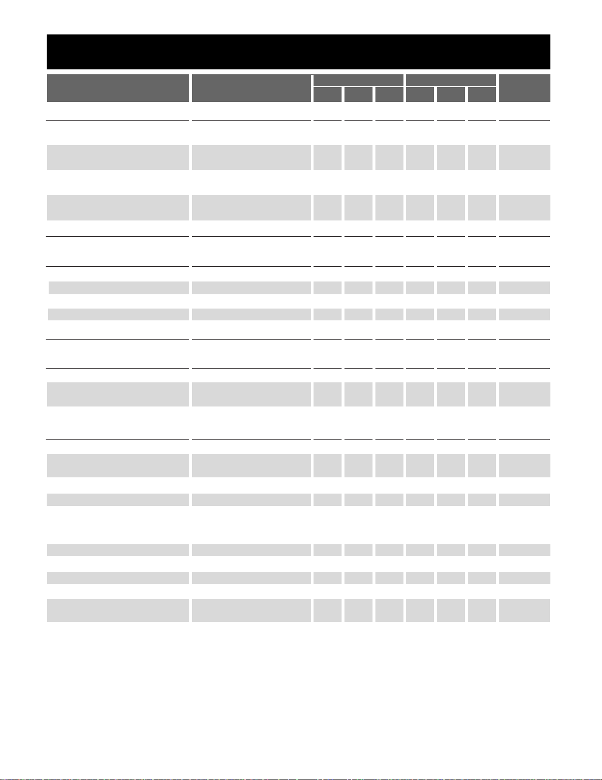
Electrical Characteristics: -30¡C ² TA² 125¡C; -30¡C < TJ< 125¡C; All Parameters after VCCPower-up > 100ms;
V
BAT
= 14V unless otherwise specified.
16 Lead SO Wide Flip Chip
PARAMETER TEST CONDITIONS MIN TYP MAX MIN TYP MAX UNIT
■ Input, Current, Delay
Positive Threshold V
BAT
= 6V 56.2 66 56.2 66 % of V
BAT
V
BAT
= 16V 56.2 66 56.2 66 % of V
BAT
Hysteresis V
BAT
= 6V 8 20.2 9 20.2 % of V
BAT
V
BAT
= 16V 8 20.2 9 20.2 % of V
BAT
I
CC
V
BAT
= 6V 1 2.75 4.5 1 2.75 4.5 mA
V
BAT
= 16V 5 12 19 5 12 19 mA
Input Impedance @10µA 70 170 400 k½
@0.1mA 70 170 400 k½
IC Process Delay 15 15 µs
■ Output
Output Current V
BAT
= 6V, 2.1V output load 40 52.5 65 40 52.5 65 mA
Output SOA Current V
BAT
= 22V (Note 1) 40 52.5 65 40 52.5 65 mA
Output Leakage Current V
BAT
= 25V (Note 1) 0 100 0 100 µA
Output Clamp Voltage @ 10mA 13.7 15.35 17 13.7 15.35 17 V
Output Clamp Impedance @ 10mA 10 42.5 80 10 42.5 80 ½
■ Regulation Voltage
VS Regulation Voltage V
BAT
= 7.8V 165 200 235 165 200 235 mV
VS Supply Rejection V
BAT
= 6V ~ 22V (Note 1) 0 0 14 0 0 14 %
V
BAT
= 7.8V ~ 22V (Note 1) 0 0 13 0 0 13 %
■ Stall & Protection
Stall Shutdown VS V
BAT
= 6V -5 0 5 -1 0 1 mV
Stall Shutdown Frequency V
BAT
= 14V .4 .4 Hz
V
BAT
= 5.5V 1.4 1.47 1.4 1.47 Hz
Stall Shutdown Time V
BAT
= 6V 19 28 37 19 28 37 ms
Stall to Spark Output Delay 4.6 6.7 9.5 4.6 6.7 9.5 ms
I/O Signal Relationship @ 80% Input 79.0 80.5 82.0 79.0 80.0 81.0 %
@ 50% Input 49.0 50.5 52.0 49.0 50.0 51.0 %
@ 30% Input 29.0 30.5 32.0 29.0 30.0 31.0 %
Battery Interrupt Time 25 750 25 750 ms
Battery Interrupt Recovery Time @ 200Hz 800 800 ms
High Voltage Shutdown 25 28 32 25 28 31 V
High Frequency Cut off 1 2.5 5 1 2.5 5 kHz
Negative Threshold V
BAT
= 6V 28 36 30 36 % of V
BAT
V
BAT
= 16V 28 36 30 36 % of V
BAT
Note 1: Voltage extremes are for testing purposes only. Part in continuous operation should conform to absolute max
table.
Page 3

CS464
3
Package Pin Description
PACKAGE PIN # PIN SYMBOL FUNCTION
Flip-Chip 16 Lead
(Bump #) SO Wide
1 13 OUT Output control of darlington driver.
2 15 S Current sense feedback input.
3 16 CS Stall timer capacitor.
4 1 MB Master current bias resistor.
5 2,3,6,7,10,14 NC No connection.
6 4 CR Reset capacitor.
7 5 IN+ Input control.
8 IN- Negative input control (grounded in 16 Lead SO package).
9 8 Gnd Ground.
10 9 V
CC
Input supply voltage.
11 11 D Darlington drive supply input.
12 12 IC Input collector voltage sense.
13 TEST Test bump, grounded.
Block Diagram
V
CC
Power
Supply
8k
V
REF
63.7k
RV
CC
330W
CR
BG
+
-
PNP Current Source Bias
VR
VBG
OVS
Negative
CR
Edge
Filter
+
-
LOGIC1
+
-
5k
100k
+
-
BG
7k
12k
VR
C Q
D
R
RMB
10.7k
MB
CR > V
+
-
VR
8.4mA
INPUT
25%
REF
STALL
I
LIMIT
CR
33.6mA25%
Combinational
VR
N1
Logic
BG
25%
25%
N2
CR
0.1mF
VR
DWELL
N3
2.55k
0.63k
CS
149mA
1.1mA
To CR, CS Current Sources
CS
0.47mF
VR
149k
P2
25%*Stall
31.9mA
VR
P1
-
+
+
-
OVS
N5
N4
13.7V
Clamp
RD
55W, 5W
D
ZD
18V
OUT
RIC2
4k
IC
RIC1
200W
S
Adjust for 6.5A Coil Current
RS1
56W
ND1
Spark Plug
ND2
RS2
0.05W, 5W
V
BAT
CV
CC
0.1mF
Gnd
RIN+
V
IN
IN+
10k
VR
BG
CS
Page 4

4
Package Specification
CS464
.525 ± .05
.0302 MAX
13X .095 ± .045
13X .165 ± .038
1.022
CA
MB
CR
.496
2.39
.356
.431
1.021
.350
.267
1.020
1.022
.279
.382
1.017
.892
.384
.209
.265
.892
2.14
0
0
0
0
CS-464
ÊFlip-ChipÊ
CS
S
OUT
IC
D
V
CC
GndIN-
IN+
Test
Note: All dimensions in millimeters.
Flip-Chip
Rev. 3/1/99 © 1999 Cherry Semiconductor Corporation
PACKAGE DIMENSIONS IN mm (INCHES)
Ordering Information
Part Number Description
CS464 Flip-Chip
CS464YDW16 16 Lead SO Wide
CS464YDWR16 16 Lead SO Wide (tape & reel)
PACKAGE THERMAL DATA
D
Lead Count Metric English
Max Min Max Min
16 Lead SO Wide 10.50 10.10 .413 .398
Thermal Data 16 Lead SO Wide
R
QJC
typ 23 ûC/W
R
QJA
typ 105 ûC/W
Bump Locations, Bump Side Up
Cherry Semiconductor Corporation reserves the right to
make changes to the specifications without notice. Please
contact Cherry Semiconductor Corporation for the latest
available information.
Surface Mount Wide Body (DW); 300 mil wide
1.27 (.050) BSC
7.60 (.299)
7.40 (.291)
10.65 (.419)
10.00 (.394)
D
0.32 (.013)
0.23 (.009)
1.27 (.050)
0.40 (.016)
REF: JEDEC MS-013
2.49 (.098)
2.24 (.088)
0.51 (.020)
0.33 (.013)
2.65 (.104)
2.35 (.093)
0.30 (.012)
0.10 (.004)
 Loading...