

Page 1
1
Features
■ Oscillator has Precise
Duty Cycle
Limit and Frequency
Control
■ 500kHz Current Mode
Operation
■ Automatic Feed Forward
Compensation
■ Separate Latching PWMs
for Cycle-By-Cycle
Current Limiting
■ Internally Trimmed
Reference with
Undervoltage Lockout
■ Switchable Second
Output
■ Two High Current Totem
Pole Outputs
■ Input Undervoltage
Lockout with Hysteresis
■ Low Start-Up and
Operating Current
Package Options
16L PDIP & SO Wide
CS3865C
High Performance Dual Channel
Current Mode Controller with ENABLE
1
SYNC
2
3
4
5
6
7
8
C
T
R
T
V
FB
1
COMP
1
Sense
1
V
OUT
1
Gnd
16
15
14
13
12
11
10
9
V
CC
V
REF
ENABLE
2
V
FB
2
COMP
2
Sense
2
V
OUT
2
Pwr Gnd
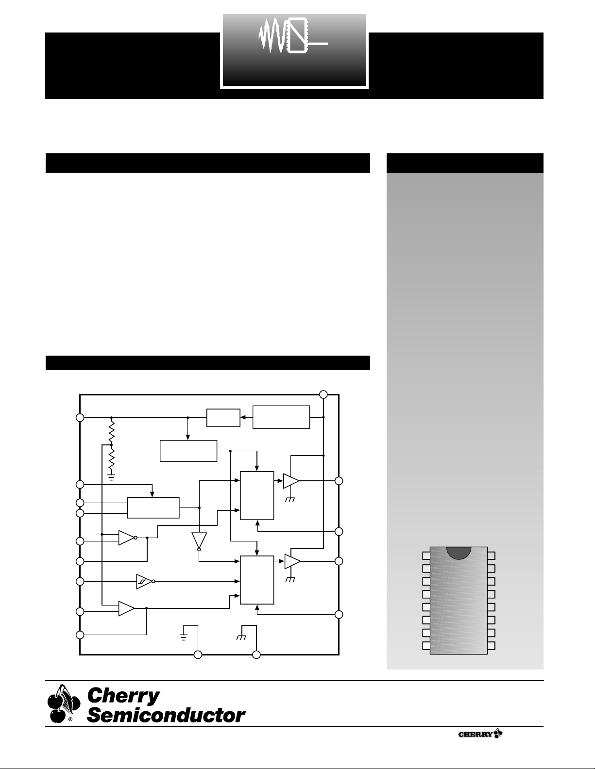
CS3865C
Description
The CS3865C is a high performance, fixed frequency, dual current mode controller. It is used in
Off-Line and DC to DC converter
applications and require a minimum number of external components. This integrated circuit features a unique oscillator for precise
duty cycle limit and frequency control, a temperature compensated
reference, two high gain error
amplifiers, two current sensing
comparators, and two high current
totem pole outputs ideally suited
for driving power MOSFETs. One
of the outputs V
OUT
2
is switchable
via the ENABLE
2
pin.
Also included are protective features consisting of input and reference undervoltage lockouts each
with hysteresis, cycle-by-cycle current limiting, and a latch for single
pulse metering of each output.
The CS3865C has a 14V start voltage and is pin compatible with the
MC34065H.
Block Diagram
Rev. 12/16/96
Cherry Semiconductor Corporation
2000 South County Trail, East Greenwich, RI 02818
Tel: (401)885-3600 Fax: (401)885-5786
Email: info@cherry-semi.com
Web Site: www.cherry-semi.com
A Company
®
V
REF
Undervoltage
Lockout
V
5.0V Ref
V
REF
CC
Undervoltage
Lockout
V
CC
SYNC
V
COMP
ENABLE
V
COMP
V
OUT
Latching
C
T
R
T
FB
1
1
2
FB
2
2
+
-
Error
Amp 1
+
-
Error
Amp 2
Oscillator
Gnd
PWM 1
Latching
PWM 2
Pwr Gnd
1
Sense
1
V
OUT
2
Sense
2
Page 2
2
Electrical Characteristics: V
CC
= 15V, RT = 8.2kΩ, CT = 3.3nF, for typical values TA=25˚C, for min/max values TAis the operating
ambient temperature range that applies [Note 3].
PARAMETER TEST CONDITIONS MIN TYP MAX UNIT
Absolute Maximum Ratings
Total Power Supply and Zener Current .........................................................................................................................50mA
Output Current, Source or Sink (Note 1)...........................................................................................................................1.0A
Output Energy (capacitive load per cycle) .......................................................................................................................5.0µJ
Current Sense, Enable and Voltage......................................................................................................................-0.3 to +5.5V
Feedback Inputs
High State (Voltage)..........................................................................................................................................5.5V
Low State (Reverse Current) ......................................................................................................................-5.0mA
Error Amp Output Sink Current......................................................................................................................................10mA
Storage Temperature Range ................................................................................................................................-65 to +150°C
Operating Junction Temperature...................................................................................................................................+150°C
Operating Ambient Temperature.............................................................................................................................0 to +70°C
Lead Temperature Soldering
Wave Solder (through hole styles only) .................................................................................10 sec. max, 260°C peak
Reflow (SMD styles only) ..................................................................................60 sec. max above 183°C, 230°C peak
CS3865C
■ Reference Section
Reference Output Voltage, I
OUT
=1.0mA, TJ=25°C 4.9 5.0 5.1 V
V
REF
Line Regulation 11V≤VCC≤15V 2.0 20.0 mV
Load Regulation 1.0mA≤I
OUT
≤10mA 3.0 25.0 mV
Total Output Variation over 4.85 5.15 V
Line, Load and Temperature
Output Short Circuit Current 30 100 mA
■ Oscillator and PWM Sections
Total Frequency Variation 11V≤VCC≤15V, T
low≤TA≤Thigh
46.5 49.0 51.5 kHz
over Line and Temperature
Frequency Change with 11V≤VCC≤15V 0.2 1.0 %
Voltage
Duty Cycle at each Output Maximum 46.0 49.5 52.0 %
Sync Input Current High State VIN=2.4V 170 250 µA
Low State VIN=0.8V 80 160
■ Error Amplifiers
Voltage Feedback Input V
OUT
=2.5V 2.42 2.50 2.58 V
Input Bias Current VFB=5.0V -0.1 -1.0 µA
Open-Loop Voltage Gain V
OUT
=2.0 to 4.0V 65 100 dB
Unity Gain Bandwidth TJ=25°C (note 6) 0.7 1.0 MHz
Power Supply Rejection Ratio VCC=11V to 15V 60 90 dB
Output Current Source V
OUT
=3.0V, VFB=2.3V -0.45 -1.00 mA
Sink V
OUT
=1.2V, VFB=2.7V 2.00 12.00 mA
Output Voltage Swing High State, RL=15k to ground,
VFB=2.3V 5.0 6.2 V
Low State, RL=15k to V
REF
,
VFB= 2.7V 0.8 1.1
Page 3

3
CS3865C
PARAMETER TEST CONDITIONS MIN TYP MAX UNIT
Note 1: Maximum package power dissipation limits must be observed.
Note 3: Adjust VCCabove the Start-Up threshold before setting to 15V.
Note 4: This parameter is measured at latch trip point with VFB=0V.
Note 5: Comparator gain is defined as:
AV =
Note 6: These parameters are guaranteed by design but not 100% tested
in production.
Note 7: Low duty cycle pulse techniques are used during test to maintain junction temperature as close to ambient as possible: T
low
=0°C ;
T
high
=+70°C
∆V Compensation
∆V Current Sense
■ Current Sense Section
Current Sense Input (Notes 4 and 5) 2.75 3.00 3.25 V/V
Voltage Gain
Maximum Current Sense (Note 4) 430 480 530 mV
Input Threshold
Input Bias Current -2.0 -10.0 µA
Propagation Delay Current Sense Input to Output (Note 6) 150 300 ns
■ Output 2 Enable Pin
Enable Pin Voltage
High State Output 2 enabled 3.5 V
REF
V
Low State Output 2 disabled 0.0 1.5 V
Low State Input Current V
IL
= 0V 100 250 400 µA
■ Drive Outputs
Output Voltage
Low State I
SINK
=20mA 0.1 0.4 V
I
SINK
=200mA 1.6 2.5 V
High State I
SOURCE
=20mA 13.0 13.5 V
I
SOURCE
=200mA 12.0 13.4 V
Output Voltage with VCC=6.0V, I
SINK
=1.0mA 0.1 1.1 V
UVLO Activated
Output Voltage Rise Time CL=1.0nF (Note 6) 28 150 ns
Output Voltage Fall Time CL=1.0nF (Note 6) 25 150 ns
■ Undervoltage Lockout Section
Start-Up Threshold CS3865C 13 14 15 V
Minimum Operating Voltage 9.0 10.0 11.0 V
After Turn-On
Hysteresis 4V
■ Total Device
Start-Up Current V
CC
=12V 0.6 1.0 mA
Operating Current (Note 7) 20 25 mA
Power Supply Zener Voltage I
CC
=30mA 15.5 17.0 19.0 V
Electrical Characteristics: V
CC
= 15V, RT = 8.2kΩ, CT = 3.3nF, for typical values TA=25˚C, for min/max values TAis the operating
ambient temperature range that applies [Note 3].
Page 4

4
CS3865C
Package Pin Description
PACKAGE PIN # PIN SYMBOL FUNCTION
Typical Performance Characteristics
100pF
1.0nF
10k 30k 50k 100k 300k 500k 1.0M
f
OSC
OSCILLATOR FREQUENCY (Hz)
4.0
6.0
8.0
10
12
14
16
R
T
TIMING RESISTOR (KΩ)
TA=25°C
2.2nF
3.3nF
5.0nF
C
T
=10nF
VCC=
15V
220pF
330pF
500pF
10k 30k 50k 100k 300k 500k 1.0M
f
OSC
OSCILLATOR FREQUENCY (Hz)
38
40
42
44
46
48
50
MAXIMUM DUTY CYCLE (%)
V
CC
= 15V
R
T
= 4.0kΩ to 16kΩ
C
L
= 15pF
T
A
= 25°C
OUT 2
OUT 1
Max. Output Duty Cycle vs. Oscillator Frequency
Timing Resistor vs. Oscillator Frequency
10k 100k 1.0k 10k 100k 1.0M 10M
f, FREQUENCY (Hz)
-20
0
20
40
60
80
100
A
VOL
, OPEN-LOOP VOLTAGE GAIN (dB)
V
CC
= 15V
V
O
= 1.5V TO 2.5V
R
L
= 100kΩ
T
A
= 25°C
GAIN
PHASE
180
150
120
90
60
30
0
Phase Margin (DEGREES)
0 1.0 2.0 3.0 4.0 5.0 7.0
ERROR AMP OUTPUT VOLTAGE (V)
0
0.1
0.2
0.3
0.4
0.5
0.6
Vth, CURRENT SENSE
INPUT THRESHHOLD (V)
6.0
V
CC
= 15V
TA = 125°C
TA = 25°C
TA = -55°C
Current Sense Input Threshold
vs. Error Amp Output Voltage
Error Amp Open-Loop Gain & Phase vs. Frequency
16 L PDIP & SO Wide
1 SYNC A positive going pulse applied to this input will synchronize the
oscillator. A DC voltage within the range of 2.4V to 5.5V will inhibit
the oscillator.
2C
T
Timing capacitor CTconnects pin to ground setting oscillator frequency.
3R
T
Resistor RTconnects to ground setting the charge current for CT. Its
value must be between 4.0k and 16k.
4V
FB
1
The inverting input of error amplifier 1. Normally it is connected to
the switching power supply output.
5 COMP
1
The output of error amplifier 1, for loop compensation.
6 Sense
1
Output 1 pulse by pulse current limit.
7V
OUT
1
Drives the power switch at output 1.
8 Gnd Logic ground
9 Pwr Gnd Power ground. Power device return is connected to this pin.
10 V
OUT
2
Drives the power switch at output 2.
11 Sense
2
Output 2 pulse by pulse current limit.
12 COMP
2
Output of error amplifier 2, for loop compensation.
13 V
FB
2
Inverting input of error amplifier 2. Normally it is connected to the
switching power supply output.
14 ENABLE
2
Output 2 disable. A logic low at this pin disables V
OUT
2
.
15 V
REF
5.0V reference output. It can source current in excess of 30mA.
16 V
CC
The positive supply of the IC.
Page 5

5
The CS3865C is a high performance, fixed frequency, dual
channel current mode PWM controller specifically
designed for off-line and DC to DC converter applications.
It offers the designer a cost effective solution with minimal
external components where independent regulation of two
power converters is required. Each channel contains a high
gain error amplifier, current sensing comparator, pulse
width modulator latch, and totem pole output driver. The
oscillator, reference, and undervoltage lockout circuits are
common to both channels.
The oscillator uses precise frequency and duty cycle control. The frequency is programmed by the values R
T
and
CT. Capacitor, CT, is charged and discharged by an equal
magnitude internal current source and sink, generating a
symmetrical 50 percent duty cycle waveform at CT. The
oscillator peak and valley thresholds are 3.5V and 1.6V
respectively. The source/sink current magnitude is controlled by resistor RT. For proper operation over temperature range, its value should be between 4.0kΩ and 16kΩ.
As CTcharges and discharges, an internal blanking pulse
is generated that alternately drives the inputs of the upper
and lower NOR gates high. This, in conjunction with a
precise amount of delay time introduced into each channel, produces well defined non-overlapping output duty
cycles. The second output, V
OUT
2
is enabled while CTis
charging, and the primary is enabled during the discharge.
Even at 500kHz, each output is capable of approximately
44% duty cycle, making this controller suitable for high
frequency power conversion applications.
In many noise sensitive applications, it may be necessary
to synchronize the converter with an external system
clock. This can be accomplished by applying an external
clock signal. For reliable synchronization, the oscillator frequency should be set about 10% slower than the clock frequency. The rising edge of the clock signal applied to
SYNC, terminates C
T
‘s charging and V
OUT
2
‘s conduction.
By tailoring the clock waveform symmetry, accurate duty
cycle clamping of either output can be achieved.
Each channel contains a fully-compensated error amplifier. The output and inverting input nodes are accessible.
The amplifier features a typical dc voltage gain of 100 dB,
and a unity gain bandwidth of 1.0 MHz with 71 degrees of
phase margin. The non-inverting input is internally biased
at 2.5V. The converter output voltage is typically divided
down and monitored by the inverting input through a
resistor divider. The maximum input bias current is -1.0µA
which will cause an output voltage error that is equal to
the product of the input bias current and the equivalent
input divider resistance.
Error Amplifier
Oscillator
Operating Description
CS3865C
Typical Performance Characteristics: continued
Reference Short Circuit Current vs. TemperatureReference Voltage Change vs. Source Current
Supply Current vs. Supply Voltage CS3865C
Output Saturation Voltage vs. Load Current
0
-4.0
-8.0
-12
, REFERENCE
Voltage (mV)
-16
REF
∆ V
-20
-24
0 20 40 60 80 100 120
I
ref
TA = 125°C
, REFERENCE SOURCE CURRENT (mA)
V
= 15V
CC
TA = –55°C
TA =
25°C
120
100
, REFERENCE
80
SC
I
SHORT CIRCUIT CURRENT (mA)
60
-55 -25 0 25 50 75 100 125
T
, AMBIENT TEMPERATURE (°C)
A
0
SOURCE SATURATION
V
(LOAD TO GROUND)
CC
-1.0
-2.0
, OUTPUT
sat
V
SATURATION VOLTAGE (V)
TA= –55°C
2.0
1.0
0
0 200 400 600 800
OUTPUT LOAD CURRENT (mA)
TA=25°C
T
A
= –55°C
GND
VCC=15V
80µS PULSED LOAD
120Hz RATE
=25°C
T
A
SINK
SATURATION
(LOAD TO V
CC
)
32
RT=8.2kΩ
T=3.3nF
C
V
1.2=0V
FB
24
CURRENT SENSE 1.2=0V
=25°C
T
A
16
8.0
SUPPLY CURRENT (mA)
CC,
I
0
0 4.0 8.0 12 16 20
SUPPLY VOLTAGE (V)
V
CC,
Page 6

6
The error amp is compensated externally thru the VFBand
COMP pins. Its output voltage is offset by two diode
drops (≈1.4V) and divided by three before it connects to
the inverting input of the current sense comparator. This
guarantees that both outputs are disabled when the error
amplifier output is at its lowest state which occurs when
the power supply is operating at light or no-load conditions, or at the beginning of a soft-start interval.
The minimum allowable error amplifier feedback resistance is limited by the amplifier’s source current capability
(0.5 mA) and the output voltage (V
OH
) required to reach
the current sense comparator 0.5V clamp level with the
error amplifier inverting input at ground. This condition
happens during initial system start up or when the sensed
output is shorted:
R
F(min)
≈
= 5800Ω
The CS3865C operates as a current mode controller.
Output switch conduction is initiated by the oscillator and
terminated when the peak inductor current reaches the
threshold level established by the error amplifier output.
Thus the error signal controls the peak inductor current on
a cycle-by-cycle basis. The current sense comparator-PWM
Latch combination ensures that only a single pulse
appears at the drive output (V
OUT
) during any given oscillator cycle. The current is converted to a voltage by connecting a sense resistor R
Sense
in series with the source of
output switch Q1 and ground. This voltage is monitored
through the Sense
1,2
pins and compared to a voltage
derived from the error amp output. The peak current
under normal operating conditions is controlled by the
voltage at COMP where:
Ipk=
Abnormal operating conditions occur when the power
supply output is overloaded or if output voltage is too
high. Under these conditions, the current sense comparator threshold will be internally clamped to 0.5V. Therefore
the maximum peak switch current is:
I
pk(max)
=
Erratic operation due to noise pickup can result if there is
an excessive reduction of the Ipk (max) clamp voltage.
A narrow spike on the leading edge of the current waveform can usually be observed and may cause the power
supply to exhibit an instability when the output is lightly
loaded. The addition of an R
C
filter on the current sense
input reduces this spike to an acceptable level.
Two undervoltage lockout comparators have been incorporated to guarantee that the IC is fully functional before
the output stages are enabled. Power supply terminal
(V
CC
) and the reference output (V
REF
) are monitored by
separate comparator. Each has built-in hysteresis to prevent erratic output behavior as their respective thresholds
are crossed. The upper and lower thresholds of the V
CC
comparator are 14V and 10V respectively.
The V
REF
comparator disables the drive outputs until the
internal circuitry is functional. This comparator has upper
and lower thresholds of 3.6V and 3.4V. A 17V zener is connected as a shunt regulator from V
CC
to ground to protect
the IC and power MOSFET gate from excessive voltage.
The guaranteed minimum operating voltage after turn-on
is 11V.
Each channel contains a single totem-pole output stage
that is specifically designed for direct drive of power
MOSFET’s. The outputs have up to ±1.0A peak current
capability and have a typical rise and fall time of 28 ns
with a 1.0nF load. Internal circuitry has been added to
keep the outputs in active pull-down mode whenever an
undervoltage lockout is active, eliminating the need for an
external pull-down resistor.
Although the outputs are optimized for MOSFET’s, they
can easily supply the negative base current required by
bipolar NPN transistors for enhanced turn-off. Since the
outputs do not contain internal current limits an external
series resistor will be required to prevent the peak output
current from exceeding the ±1.0A maximum rating. The
sink saturation (V
OL
) is less than 0.4V at 100mA.
A separate ground pin, Pwr Gnd, is provided. Properly
implemented, will significantly reduce the level of switching transient noise imposed on the control circuitry. This
becomes important when the I
pk(max)
clamp level is
reduced.
This input is used to switch V
OUT
2
. V
OUT
1
is used to control
circuitry that runs continuously, e.g. volatile memory, the
system clock, or a remote controlled receiver. V
OUT
2
output can control the high power circuitry that is turned off
when not needed.
The 5.0V bandgap reference is trimmed to ±2.0% tolerance. The reference has short circuit protection and is
capable of sourcing 30mA for powering any additional
external circuitry.
Voltage Reference
ENABLE
2
Outputs and Power Ground
Undervoltage Lockout
0.5V
R
Sense
V(COMP) – 1.4V
3R
Sense
Current Sense Comparator and PWM Latch
3 x 0.5V + 1.4V
0.5mA
Operating Description continued
CS3865C
Page 7

7
High frequency circuit layout techniques are imperative to
prevent pulse-width jitter. This is usually caused by excessive noise pick-up imposed on the current sense and voltage feed-back inputs. Noise immunity can be improved by
lowering circuit impedances at these points. The printed
circuit board layout should contain a ground plane with
low current signal and high current switch and output
grounds returning on separate paths back to the input fil-
ter capacitor. Ceramic bypass capacitors (0.1µF) connected
directly to V
CC
and V
REF
may be required to improve noise
filtering. They provide a low impedance path for filtering
the high frequency noise. All high current loops should be
kept as short as possible using heavy copper runs. The
error amp compensation circuitry and the converter output voltage-divider should be located close to the IC and
as far as possible from the power switch and other noise
generating components.
Design Considerations
Operating Description: continued
Applications Diagram
CS3865C
Timing Diagram
SYNC
Latch 1
“Set” Input
COMP
Sense
Latch 1
“Reset” Input
V
OUT
ENABLE
Latch 2
“Set” Input
COMP
Sense
Latch 2
“Reset” Input
V
OUT
C
T
1
1
1
2
0V
2
2
2
Dual Boost Regulator
V
CC
5.0V
C
F2
V
REF
2.5V
R
Internal
Bias
R
Sync
V
OUT
1
R
T
C
COMP
ENABLE
3
4
COMP
T
V
FB
1
1
2
V
FB
2
2
R
FB
1
R
FB
2
V
OUT
2
R
FB
R
FB
Error
Amp 1
Error
Amp 2
+
-
+
-
+
1.0mA
250µA
+
1.0mA
Oscillator
2R
+
0.5V
Current Sense
Comparator 1
2R
0.5V
Current Sense
Comparator 1
R
R
3.4V
20kΩ
+
-
+
-
Reference
Regulator
+
-
PWM
Latch 1
PWM
Latch 2
+
-
UVLO
S
R
S
R
R
UVLO
V
REF
Q
Q
17V
+
+
V
CC
14V
-
C
F1
V
OUT
Sense
V
OUT
Sense
V
IN
+
L
1
Q1
1
R
Sense
1
D
1
L
2
D
2
1
V
OUT
OUT
OUT
1
1
V
OUT
2
2
+
C
+
C
Q2
2
2
R
Sense
2
Gnd
Pwr Gnd
Page 8

8
Thermal Data 16 Lead 16 Lead
PDIP SO
RΘ
JC
typ 42 23 ˚C/W
RΘ
JA
typ 80 105 ˚C/W
D
Lead Count Metric English
Max Min Max Min
16L PDIP 19.69 18.67 .775 .735
16L SO 10.50 10.10 .413 .398
Package Specification
PACKAGE DIMENSIONS IN mm (INCHES)
Ordering Information
PACKAGE THERMAL DATA
Rev. 12/16/96
CS3865C
Part Number Description
CS3865CGN16 16L PDIP
CS3865CGDW16 16L SO Wide
CS3865CGDWR16 16L SO Wide (tape & reel)
© 1999 Cherry Semiconductor Corporation
Cherry Semiconductor Corporation reserves the
right to make changes to the specifications without
notice. Please contact Cherry Semiconductor
Corporation for the latest available information.
1.27 (.050) BSC
7.60 (.299)
7.40 (.291)
10.65 (.419)
10.00 (.394)
D
0.32 (.013)
0.23 (.009)
1.27 (.050)
0.40 (.016)
REF: JEDEC MS-013
2.49 (.098)
2.24 (.088)
0.51 (.020)
0.33 (.013)
2.65 (.104)
2.35 (.093)
0.30 (.012)
0.10 (.004)
Surface Mount Wide Body (DW); 300 mil wide
Plastic DIP (N); 300 mil wide
0.39 (.015)
MIN.
2.54 (.100) BSC
1.77 (.070)
1.14 (.045)
D
Some 8 and 16 lead
packages may have
1/2 lead at the end
of the package.
All specs are the same.
.203 (.008)
.356 (.014)
REF: JEDEC MS-001
3.68 (.145)
2.92 (.115)
8.26 (.325)
7.62 (.300)
7.11 (.280)
6.10 (.240)
.356 (.014)
.558 (.022)
 Loading...