

Page 1
Features
■
Adjustable Battery Sense
from 7 to 12 Volts
■
Pulse Loads Battery at up
to 50mA
■
Standby Current Under
10µA
■ Test Period, Rate and Load
Adjustable
■ On Chip 15mA Output
Driver
Package Options
8L PDIP and 8L SO
CS2516
Pulse-Load Battery Monitor
CS2516
Description
The CS2516 is designed for use in battery powered medical, security, or
environmental systems where prior
notification of impending power
source failure is a requirement. The IC
effectively provides continuous monitoring of battery condition by pulsesampling the system voltage at predetermined intervals. Low standby current permits unswitched connection to
the battery with minimal impact on
operating life. The ability to load the
battery during the test pulse provides
assurance that sufficient reserve capacity exists to operate critical system
components.
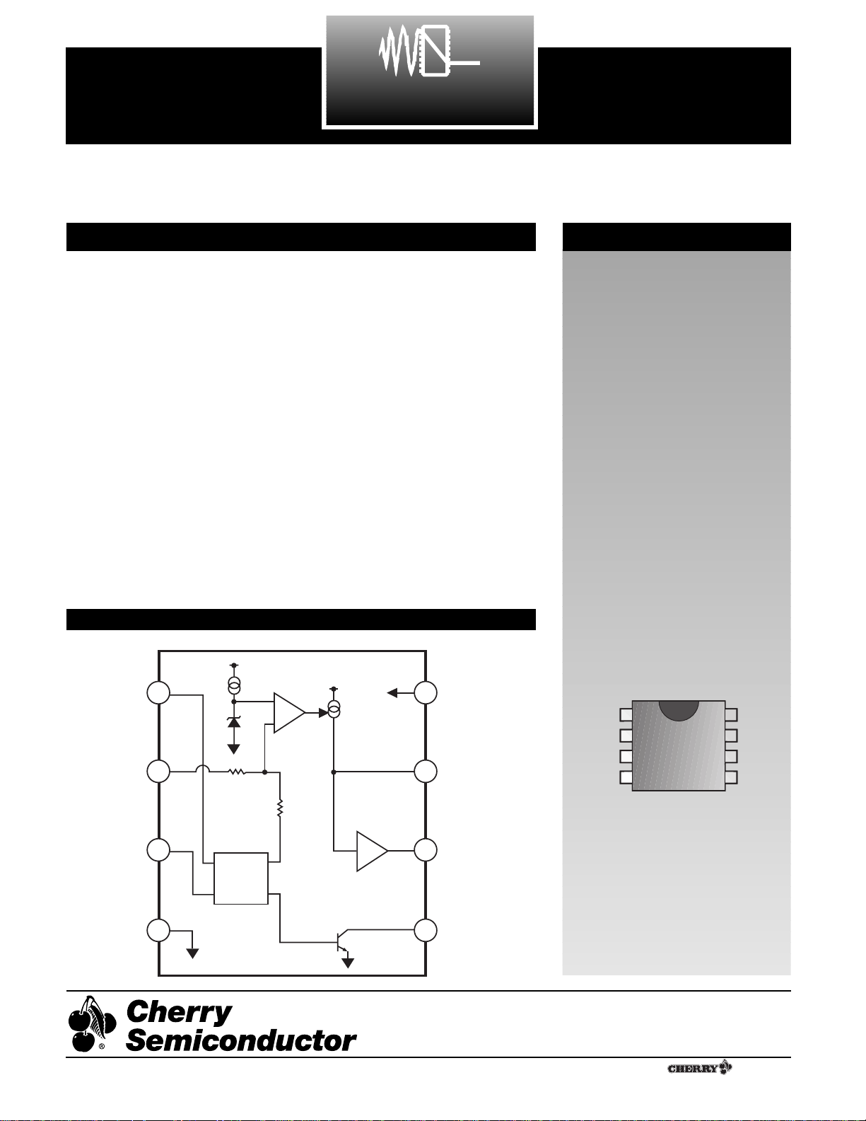
The CS2516 contains an internal timer
that generates a 1.0 millisecond test
pulse once each 33 seconds (both times
are typical). The load switch transistor
conducts only during the test pulse,
and can sink up to 50mA directly. An
external transistor can be added to increase the load current capability.
Should, during the test pulse, the sense
terminal voltage fall below the threshold level determined by the internal
(synthesized) temperature compensated zener diode, the comparator will
permit a charging current to flow out
of PW. This pin is also the input of a
Schmitt trigger that in turn drives the
output transistor. Collectively, the
charge current and trigger, in conjunction with an external RC network,
operate as a Òpulse-stretcherÓ to provide output ÒONÓ times that are a
multiple of the sampling time. This
feature permits low battery alarm
devices or visible annunciators to be
driven directly by the IC. The maximum permissible output current is
30mA.
Block Diagram
1
Cherry Semiconductor Corporation
2000 South County Trail, East Greenwich, RI 02818
Tel: (401)885-3600 Fax: (401)885-5786
Email: info@cherry-semi.com
Web Site: www.cherry-semi.com
A Company
¨
Rev. 1/17/95
R
SENSE
C
COM
V
CC
PW
OUT
Load Switch
1
R
P
SENSE
2
3
C
T
4
COM
8
7
6
5
V
CC
PW
OUT
Load
Switch
p
T
Cycle
Timer
Page 2
2
Electrical Characteristics: VCC= 9V, Rp= 9.1 M½, CT= 4.7µF, Cpw = 0.1µF, Rpw = 10M½,
0¡²TA² 85¡ unless otherwise specified.
PARAMETER TEST CONDITIONS MIN TYP MAX UNIT
Absolute Maximum Ratings
Supply Voltage (VCC).........................................................................................................................................................0 to 14V
RpInput Voltage ............................................................................................................................................................-0.5 to V
CC
SENSE, CT, PW, Output and Load Switch....................................................................................................................-0.5 to 8V
Load Current...........................................................................................................................................................................50mA
Output Current ......................................................................................................................................................................30mA
Storage Temperature.................................................................................................................................................-40 to +150ûC
Lead Temperature Soldering: Wave Solder (through hole styles only)..........................................10 sec. max, 260¡C peak
Reflow (SMD styles only) ..........................................60 sec. max above 183¡C, 230¡C peak
CS2516
■ V
CC
Operating Voltage 9 12 V
Standby Current 4 10 µA
■ Cycle Timer
Charge Current V
C
T
=0V, 6V²VCC²12V -1.70 -1.20 -0.48 µA
2V ² V
C
T
< 7.5V -0.77 -0.74 -0.71 µA
Discharge Current V
C
T
= 8.8V 8.0 20.0 25.0 mA
V
C
T
= 2.0V 1.1 3.0 3.6 mA
Discharge Impedance 4.6V < V
C
T
< 8.0V 440 ½
Upper Charge Threshold -0.48µA < I
C
T
< -1.70µA 7.0 8.0 9.0 V
Lower Charge Threshold -0.48µA < IC< -1.70µA 0.5 1.0 3.0 V
Lower Discharge Threshold 1.1mA < IC< 25mA 2.0 4.6 6.0 V
■ Load Switch
ÒONÓ Voltage I
Load Switch
= 50mA 0.3 0.5 V
ÒOFFÓ Current V
Load Switch
= 12V 1.0 µA
■ Sense Input
Threshold Voltage 6.3 6.7 7.1 V
Threshold Temp Coefficient 0¡C < TA< 85¡C 150 ppm/¡C
Active Impedance 5.0 8.5 12.0 k½
■ Pulse Stretcher
Source Current V
SENSE
= 6.3V, VPW= 0V -950 -550 -250 µA
V
CC=VSENSE
=6.3V, VPW= 0V -300 -250 -200 µA
Schmitt Upper Threshold 2.25 2.50 2.75 V
Hysteresis 0.60 1.00 1.40 V
Input Bias Current V
SENSE
=7.1V, VPW=1.2V 1.00 µA
■ Output Switch
ÒONÓ Voltage VPW= 3V; I
OUT
= 15mA 0.1 0.5 V
ÒOFFÓ Current V
PW
= 0V; V
OUT
= 12V 1.0 µA
Page 3

3
Package Pin Description
PACKAGE PIN # PIN SYMBOL FUNCTION
Typical Performance Characteristics
Timing Diagram
CTDischarge Impedance vs CTVoltage (Typ +25¡C)
Electrical Characteristics: VCC= 9V, RP= 9.1 M½, CT= 4.7µF, Cpw = 0.1µF, Rpw = 10M½,
0¡²TA² 85¡ unless otherwise specified
PARAMETER TEST CONDITIONS MIN TYP MAX UNIT
CS2516
8L PDIP & SO Narrow
1RPTest period programming resistor.
2 SENSE Voltage sense comparator input.
3CTTest period, duration programming capacitor.
4 COM Common negative
5 Load Switch Collector of pulse loading NPN transistor.
6 OUT Alarm Pulse width-stretcher output
7 PW Output pulse-width programming RC.
8VCCPower source.
■ Recommended Component Values
Rp Program Resistor 1.0 9.1 M½
C
T
Cycle Timer Capacitor 4.7 22.0 µF
CPWPulse Stretcher Capacitor 0.01 0.10 µF
RPWPulse Stretcher Resistor 1 10 M½
V
Load
Switch
PW
OUT
1000
900
800
700
Impedance, W
600
500
400
8.8 8.0 7.0 6.0 5.0 4.0 3.0 2.0 1.0
CC
C
T
1V
V
CC
0V
V
CC
7.1V
T
V
sat
8V
4.6V4.6V
p
1.14ms
BATT. OK
CT Voltage
33S
T
t
1V
6.7V
V
CC
1V
V
CC
T
d
T
pw
V
sat
1ms
510ms
BATT. LOW
2.5V
1.5V
0V
V
CC
Page 4
4
Program and Standby Currents: I
P
= = Å 1µA Standby Current = 4IP= 4µA (typ.)
9V
9.1m½
V
CC
R
P
Test Pulse Width: Tp= RdCT x ln(VP) Å 242CTÅ 242 x 4.7µF Å 1.14ms
where R
d
is the dynamic cycle timer discharge impedance (440½ typ.)
and V
P
=
[1n(VP) = 0.55 typ.]
Pulse Stretcher: Delay Time: T
D
= = = Å 1ms
where V
d
= Schmitt Trigger Upper Threshold (2.5V typ.)
and I
src
= Typical source current at the PW pin at the nominal low battery sense threshold of 6.7V.
Pulse Width: T
p
= CPWRPWln(VS) Å 0.51 x 0.1µF x 10m½ Å 510ms.
and V
S
= [ln(VS) = 0.51 typ.]
Schmitt Trigger Upper Threshold
Schmitt Trigger Hysteresis
2.5 x 0.1µF
250µA
2.5C
PW
250µA
VdC
PW
I
src
Upper Charge Threshold
Lower Discharge Threshold
Applications Information
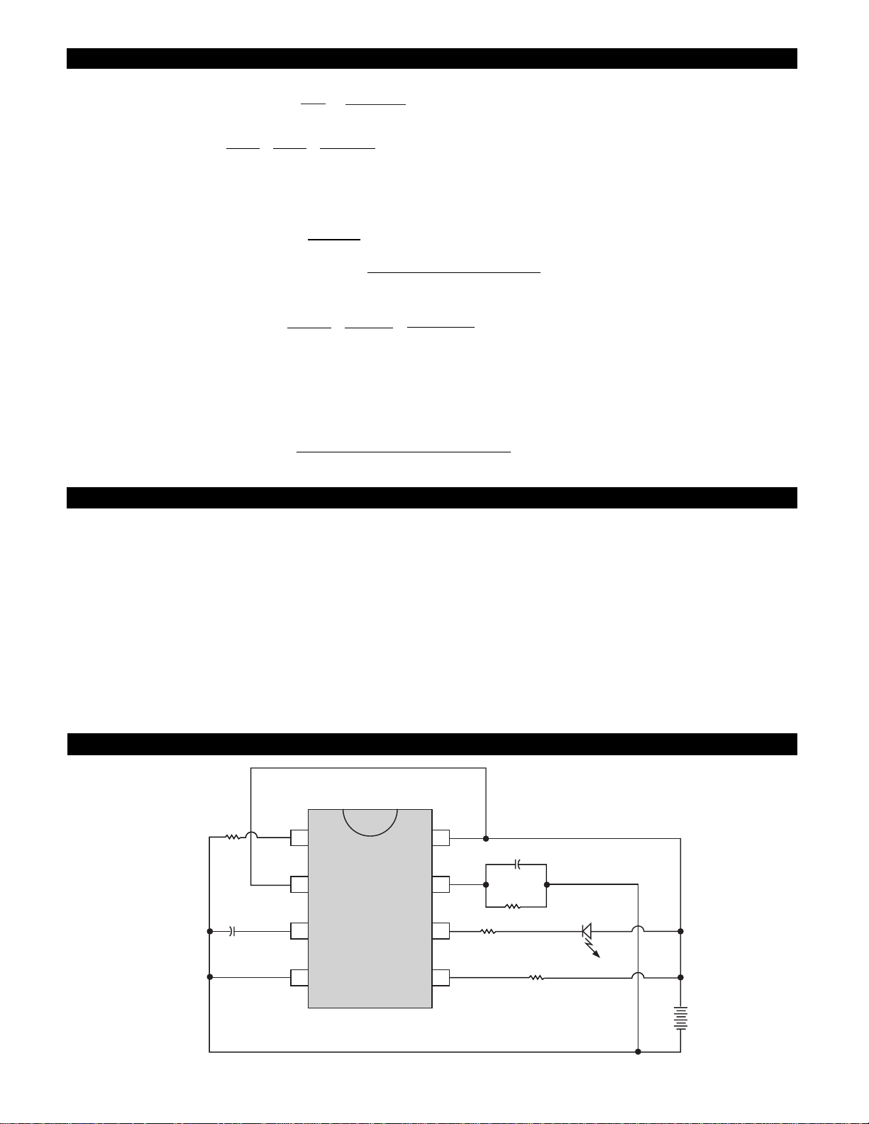
Typical Application Circuit
The value of Rpaffects standby current, operating current,
and the test cycle period. The recommended value is
(V+/1µA) where V+ is the fresh battery voltage. Higher
values of Rpare not recommended. Minimum recommended value is (V+/10µA) which will increase both the
standby and operating currents by 10X and reduce the test
cycle period by the same factor; the test pulse width will
be unaffected.
The value of Ctaffects both the test cycle period and the
test pulse width. Of critical importance is the selection of a
low leakage type capacitor; if leakage current exceeds the
cycle timer charge current, the timer will not operate.
The pulse stretcher components RPWand CPWshould be
selected such that the delay timer to charge CPWis shorter
than the test pulse width programmed by Ctto guarantee
operation of the Output. The output is an open-collector
transistor which may be used to drive an indicator device
directly or to interface to logic family devices.
The SENSE input typical 8.5k½ input impedance appears
only during the test pulse; otherwise the SENSE input is in
a high impedance state. The effective low battery threshold voltage can be modified (increased only) by means of a
voltage divider placed across the load resistor. This technique can also be used to effectively reduce the threshold
tolerance band.
Applications Formulae and Typical Values
CS2516
Cycle Timer Period: Tt=== Å 33sec.,
where V
t
= Upper Charge Threshold - Lower Charge Threshold (7V typ.)
7 x 4.7µF
1µA
7C
T
1µA
VTC
T
I
P
R
p
9.1MW
C
T
4.7mF
+
R
p
SENSE
C
T
CS2516
V
510W
CC
C
0.1mF
R
pw
10MW
pw
V
CC
PW
OUT
COM
Load Switch
220W
+
9V
Page 5
5
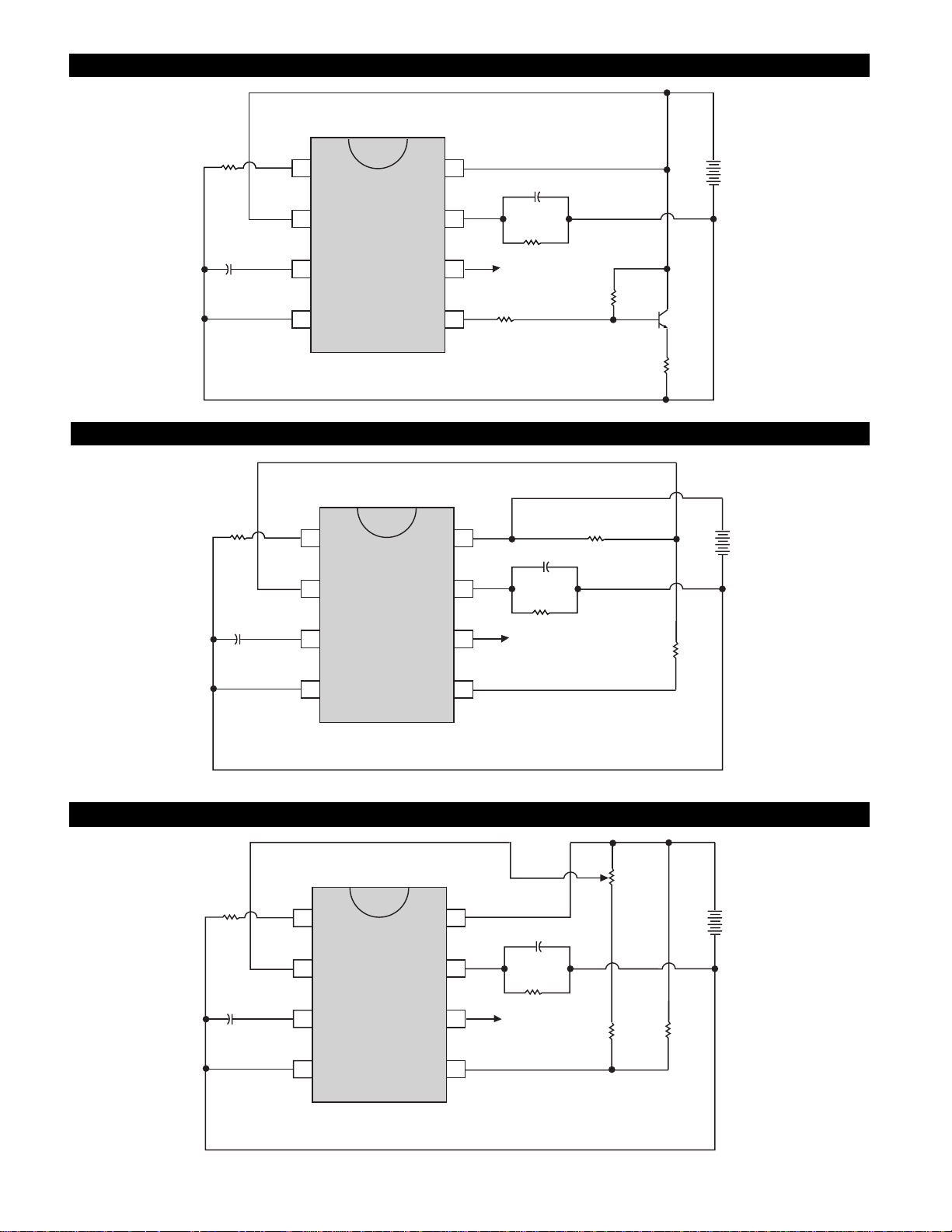
Adjustable Sense Threshold
12V Battery Application with 9V Threshold
Increased Pulse-Load Current Capability
CS2516
R
p
9.1MW
C
T
4.7mF
R
9.1MW
C
4.7mF
R
p
SENSE
CS2516
+
C
T
V
CC
PW
OUT
10MW
OUT
C
0.1mF
R
pw
pw
+
9V
820W
COM
Load Switch
220W
R
L
p
R
p
V
CC
C
SENSE
T
+
CS2516
C
T
PW
OUT
0.1mF
R
10MW
OUT
51W
pw
pw
+
12V
150W
R
9.1MW
C
4.7mF
COM
Load Switch
200W
R
L
220W
+
9V
p
R
p
SENSE
T
+
C
CS-2516
T
COM
V
CC
PW
OUT
Load Switch
OUT
C
pw
0.1mF
R
pw
10MW
1.8kW
Page 6
Part Number Description
CS2516KN8 8 Lead PDIP
CS2516KD8 8 Lead SOIC
CS2516KDR8 8 Lead SOIC (tape & reel)
6
D
Lead Count Metric English
Max Min Max Min
8L PDIP 10.16 9.02 .400 .355
8L SOIC 5.00 4.80 .197 .189
Thermal Data 8L PDIP 8L SO
RQ
JC
typ 52 45 ûC/W
RQ
JA
typ 100 165 ûC/W
Package Specification
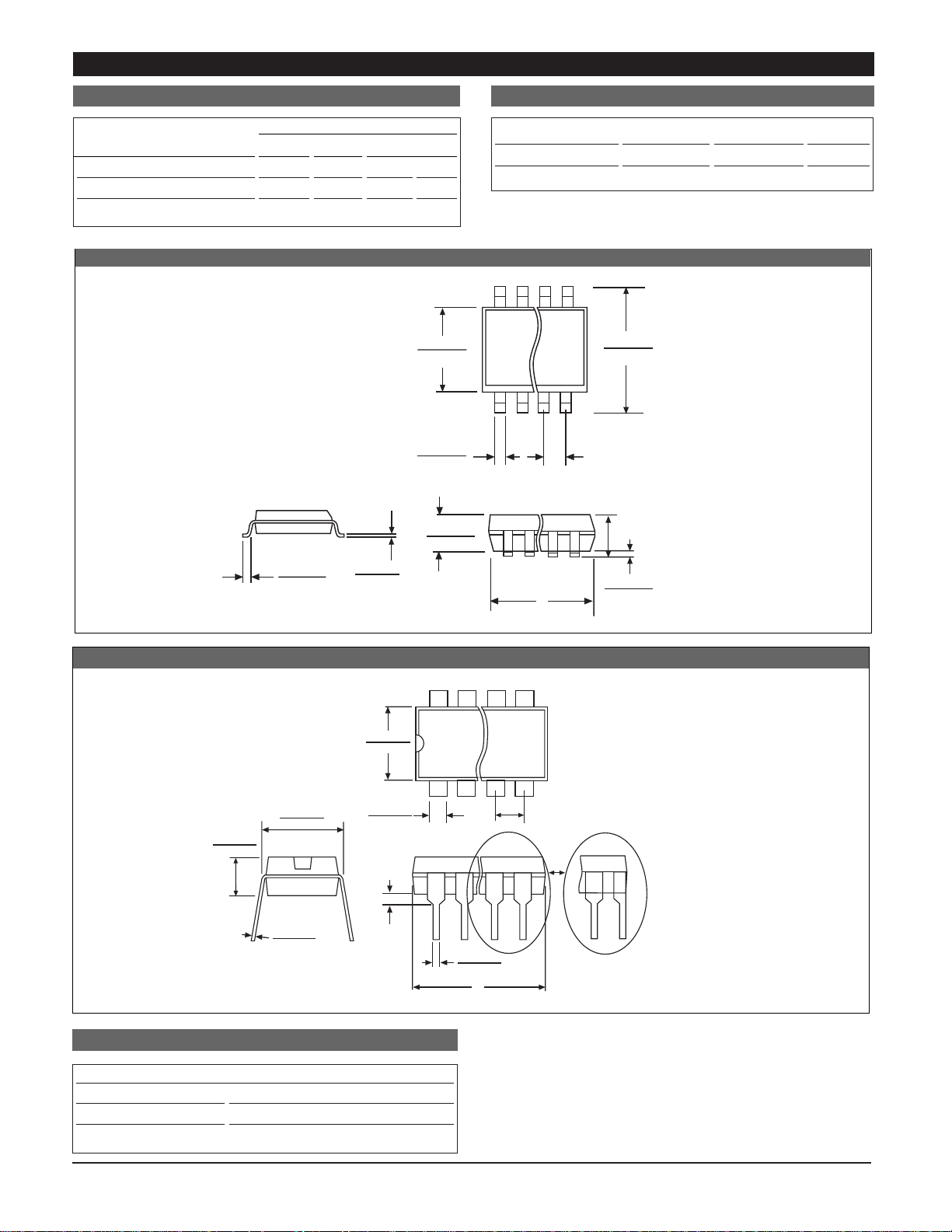
PACKAGE DIMENSIONS IN mm (INCHES)
Ordering Information
PACKAGE THERMAL DATA
Rev. 1/17/95
CS2516
© 1999 Cherry Semiconductor Corporation
Cherry Semiconductor Corporation reserves the
right to make changes to the specifications without
notice. Please contact Cherry Semiconductor
Corporation for the latest available information.
1.27 (.050) BSC
0.51 (.020)
0.33 (.013)
6.20 (.244)
5.80 (.228)
4.00 (.157)
3.80 (.150)
1.57 (.062)
1.37 (.054)
D
0.25 (0.10)
0.10 (.004)
1.75 (.069) MAX
1.27 (.050)
0.40 (.016)
REF: JEDEC MS-012
0.25 (.010)
0.19 (.008)
Surface Mount Narrow Body (D); 150 mil wide
Plastic DIP (N); 300 mil wide
0.39 (.015)
MIN.
2.54 (.100) BSC
1.77 (.070)
1.14 (.045)
D
Some 8 and 16 lead
packages may have
1/2 lead at the end
of the package.
All specs are the same.
.203 (.008)
.356 (.014)
REF: JEDEC MS-001
3.68 (.145)
2.92 (.115)
8.26 (.325)
7.62 (.300)
7.11 (.280)
6.10 (.240)
.356 (.014)
.558 (.022)
 Loading...