

Page 1
CRF-22010-TB
© Cree, Inc. 2003 Specifications subject to change without notice
Rev 1.01 - March 28, 2003 http://www.cree.com/
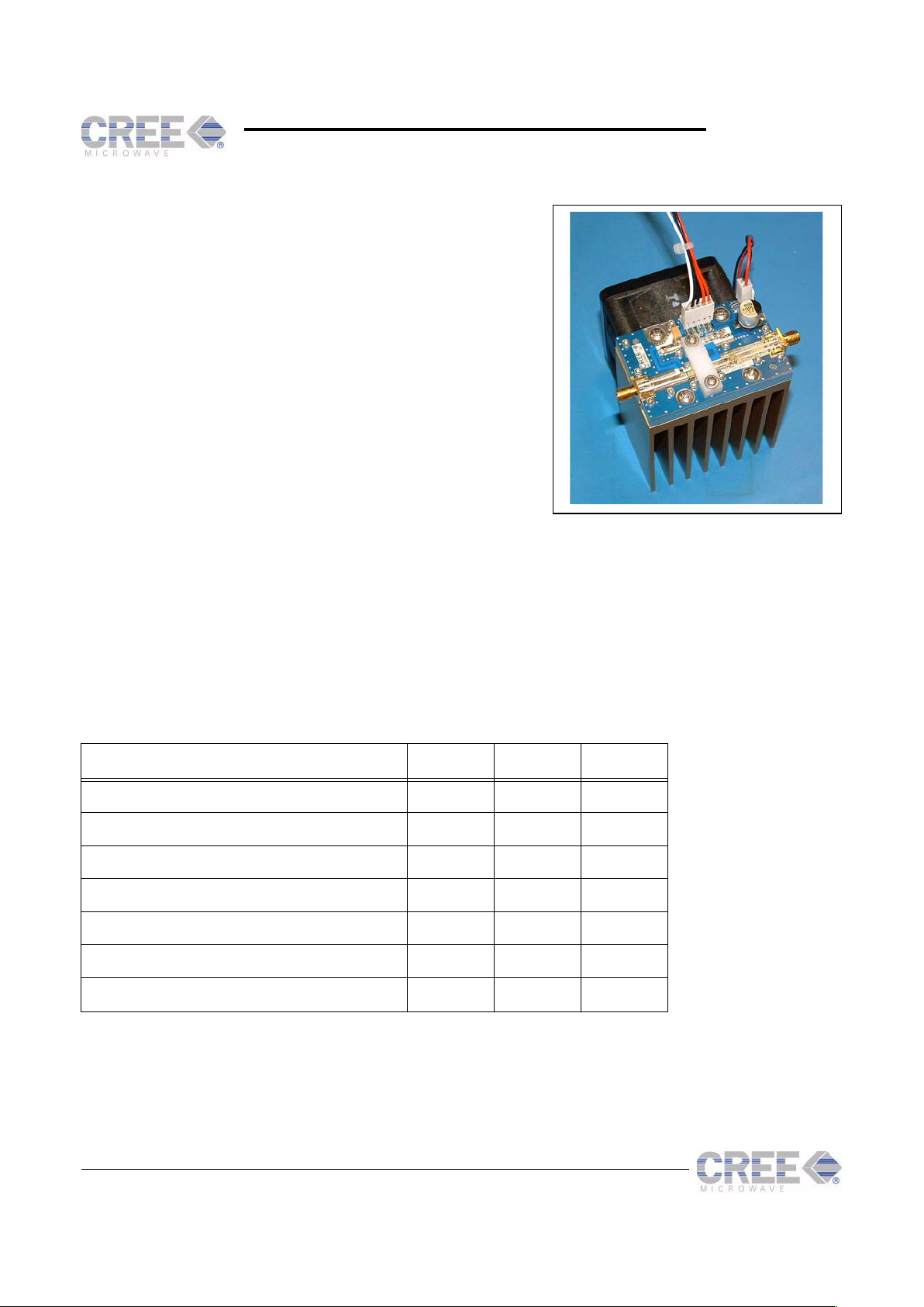
Evaluation Board for CRF-22010
Version A (Narrowband)
Features
• Ready-to-Go RF Amplifier
• Requires Two Power Supplies
• Externally Adjustable Gate Bias Voltage
• Solderless Transistor Changeout
• Includes Heat Sink, Fan, and Wiring Harness
• Designed for Narrowband Operation
Description
Cree’s CRF-22010-TB-A is a complete 10 watt RF single band power amplifier. The evaluation board is pretuned
for a specified frequency (generally between 1.8 and 2.2 GHz) and is supplied with CRF-22010 silicon carbide
MESFETs in the 101 style flange-mount package. The CRF-22010-TB-A requires a positive 48 VDC drain power
supply and a negative adjustable gate power supply (capable of providing up to -15 VDC) for operation. This board
will assist the designer in testing and evaluating the CRF-22010.
1
Amplifier and carrier without heatsink and fan assembly
Absolute Maximum Ratings (not simultaneous) at 25°C
Parameter Symbol Rating Units
Drain Supply Voltage V
DSMAX
50 VDC
Drain Supply Current I
DSMAX
+2 ADC
Gate Supply Voltage V
GSMAX
-15 VDC
Gate Supply Current I
GSMAX
0.1 ADC
Total Device Dissipation P
D
66 W
Storage Temperature T
STG
125 °C
Thermal Resistance, Junction to Base
1
R
qJB
4.5 °C/W
Page 2
CRF-22010-TB
© Cree, Inc. 2003 Specifications subject to change without notice
2 http://www.cree.com/
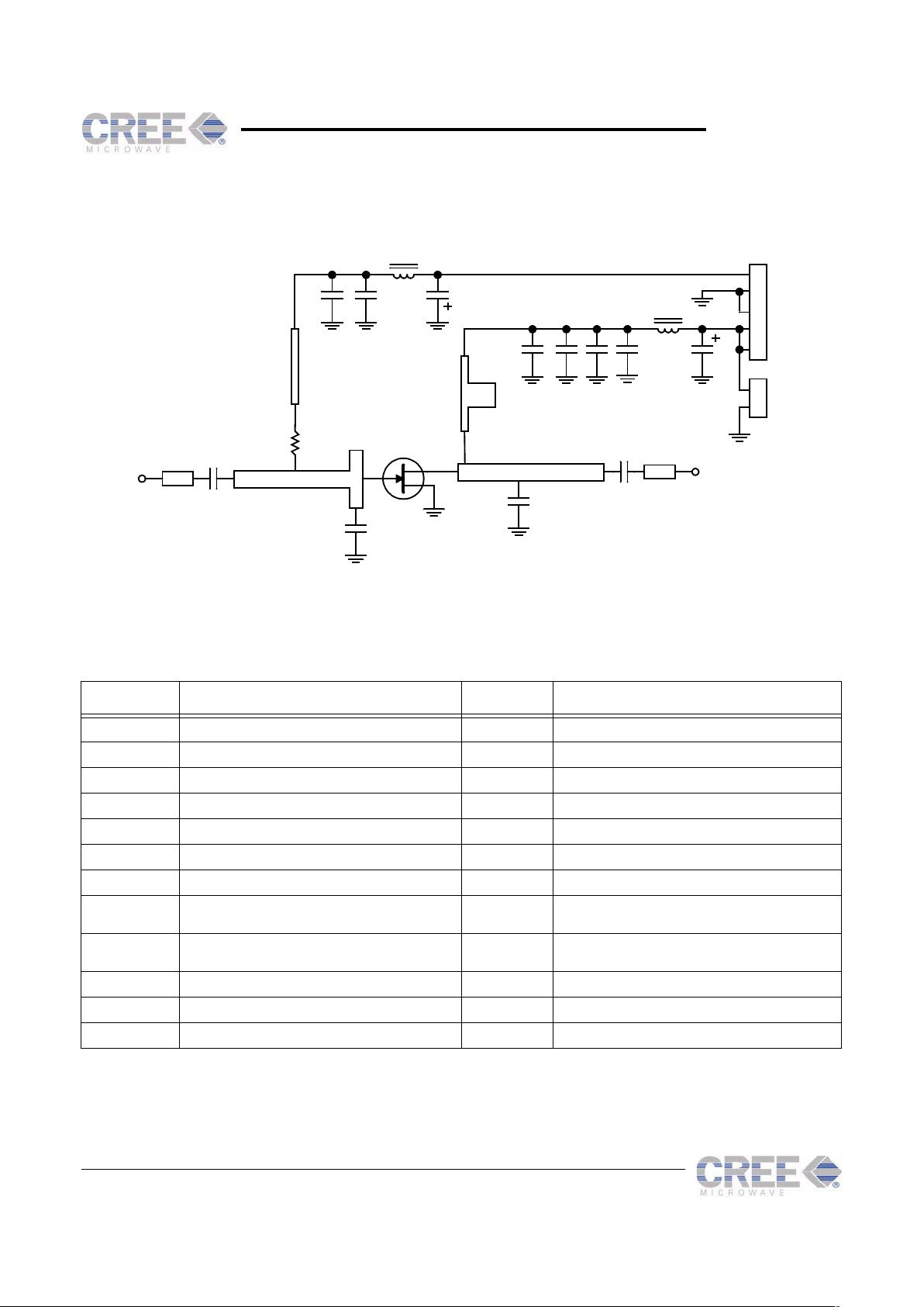
Schematic (Rev. A)
Parts List
Note: Some values may differ due to substitution in the event of temporarily unavailable parts
Designator Value Designator Value
R1 39 W, 0.1 W, 0805 Chip Resistor C1, C2, C3, C6 27 pF, 100V Ceramic Capacitor, ATC 12061C104MAT2A
L1 Ferrite, 80 ohms, Steward HI1206K101R C4 0.1 uF, 25V, 0805 Ceramic Capacitor
L2 Ferrite, Murata BLM21P220SG C5 10 uF, 25V Tantalum Capacitor
J1, J2 Flange Mount SMA Female Connector C7 2.2 nF, 100V Ceramic Capacitor, AVX 08051C222MAT2A
J3 5-pin Molex Male Connector C8 10 nF, 100V, 0805 Ceramic Capacitor
J4 2-pin Molex Male Connector C9 0.1 uF, 100V, 1206 Ceramic Capacitor
Q1 CRF-22010 C10 33 uF, 100V, Aluminum Electrolytic Capacitor
Substrate Rogers RO4003, e
r
=3.38, h=32 mil C11 3.3 pF, 150V Porcelain Capacitor, ATC
100B3R3OBW500X (exact value depends on tuning)
Heatsink Thermalloy 74605 Extrusion, 2 in long C12 2.2 pF, 150V Porcelain Capacitor, ATC
100B2R2OBW500X (exact value depends on tuning)
Fan Comair-Rotron FS48B3, 60 mm, 48V, 0.05 A, 18 cfm
V_DD
C1
C2
C3
C6 C9
C8
L1
C10
J4
J3
C7
C11
C12
C5
L2
J1
RF
IN
J2
RF
OUT
Q1
R1
V_GG
C4
FAN+
FAN-
GND
GND
V_DD
2
1
5
4
3
2
1
Page 3

CRF-22010-TB
Specifications subject to change without notice© Cree, Inc. 2003
http://www.cree.com/3
Layout
Operating Instructions
As per normal RF amplifier operation, observe correct polarity . Do not power up the evaluation board
unless the RF input and output ports are properly terminated.
The CRF-22010-TB-A is supplied fully assembled but without any transistors installed; since they are ESD-sensitive devices, they are packaged separately in protective packaging. The test board is only designed for use with
the flange style package. To install a transistor, remove the plastic clamp. Place the transistor into the cavity with
the angled gate lead towards the input connector J1. Use the two 2-56 hex screws and washers to attach the
flange to the board. Replace the clamp and retighten to effect positive contact between the circuit’s microstrip
lines and the part’s leads. Reverse this procedure to remove the device.
The evaluation board is fastened to an aluminum carrier to provide heat spreading and sinking, but this thermal
mass is not a sufficient heat sink for extended (i.e., for more than 30 seconds) operation. An optional heatsink and
fan assembly is supplied with the fixture. A thermal compound such as Wakefield #120-2 should be used at the
carrier-to-heatsink interface to ensure adequate heat transfer. Thermal compound should be used sparingly in
order to minimize the thermal drop across the interface; refer to manufacturer instructions for proper application of
thermal compound. Failure to provide adequate heatsinking will result in RF performance degradation and/
or component failure.
Q1
R1
L1
L2
C1
C2
C3
C4
J1
RF IN
J2
RF OUT
J4
FAN
J3
DC SUPPLY
C11
C5
C6
C7 C8
C9
C10
C12
Page 4

CRF-22010-TB
© Cree, Inc. 2003 Specifications subject to change without notice
4 http://www.cree.com/
Handle and test the board in an ESD-protected environment. With all power off, connect the RF and DC cables.
Standard SMA cables will mate to the RF input and output connectors. Connect an external 48 VDC power supply
to the board’s GROUND and DRAIN plugs. The supply should be capable of supplying 1.5 A minimum. Connect
an external adjustable supply to the board’s GROUND and GATE plugs. Observe correct polarity: the GATE
voltage is negative with respect to ground, and the DRAIN voltage is positive with respect to ground. Observe
proper supply sequencing: the negative gate voltage must be turned on before the positive drain voltage.
Adjust the gate voltage so that the CRF-22010 will be operating Class A at V
DS
= 48 V and IDS ~ 500 mA for initial
checkout.
Connect a 20 dBm, 2.0 GHz source to RF IN and measure output power at RF OUT. The 1 dB gain compression
point should be reached with an input power of 27 dBm to 30 dBm.
Note that, for convenience, the fan uses the board’s 48VDC supply through J4. For monitoring drain current from
the V_DD supply lead, the fan should either be disconnected and supplied separately, or its operating current
should be determined without a transistor installed in the fixture and then subtracted from later measured current
values.
Theory of Operation
Refer to the schematic presented earlier. This circuit is intended only for test and evaluation purposes; it is
not a complete, ready-for-production amplifier.
C1 and C2 are DC blocking capacitors. C11 and the transmission line to which it is connected constitute the input
match. This matching network transforms 50W to the desired source impedance (see the CRF-22010 data sheet).
Likewise C12 and the transmission line to which it is connected transform the desired load impedance to 50W.
These are lowpass matching structures, and they perform impedance matching in the desired band, but they only
give a high-Q, narrowband match. Gate bias is provided through a typical l/4 line; R1 helps to isolate and stabilize
the amplifier. C3 and C4 terminate the line in an RF short, and L1 and C5 provide further supply isolation. Drain
bias is provided through a l/4 line also, but the combination of C8-C10, L2, and the stub in the drain supply line
provide both an RF short and a termination with good video bandwidth. DC is supplied to the test board through
J3, and the fan draws its power through J4.
Some typical swept power and frequency measurements of an evaluation board are presented on the next page.
These data are measured using a typical evaluation board with a typical transistor.
Page 5

CRF-22010-TB
Specifications subject to change without notice© Cree, Inc. 2003
http://www.cree.com/5
Typical Performance at V
DS
= 48V, I
DQ
= 500mA
Swept CW Data vs Frequency
5
6
7
8
9
10
11
12
13
14
15
1.7 1.8 1.9 2 2.1 2.2 2.3
Frequency (GHz)
Gain (dB)
32
33
34
35
36
37
38
39
40
41
42
P1dB (dBm)
Swept CW Data vs Power at 1900 MHz
22
24
26
28
30
32
34
36
38
40
42
10 12 14 16 18 20 22 24 26 28 30 32
Pin (dBm)
Pout (dBm)
0.00
4.00
8.00
12.00
16.00
20.00
24.00
28.00
32.00
36.00
40.00
h
(Drain Efficiency) (%)
Page 6

CRF-22010-TB
© Cree, Inc. 2003 Specifications subject to change without notice
6 http://www.cree.com/
Disclaimer: Specifications are subject to change without notice. Cree, Inc. believes the information contained
within this data sheet to be accurate and reliable. However, no responsibility is assumed by Cree for its use or for
any infringement of patents or other rights of third parties which may result from its use. No license is granted by
implication or otherwise under any patent or patent rights of Cree. Cree makes no warranty, representation or
guarantee regarding the suitability of its products for any particular purpose. “Typical” parameters are the average
values expected by Cree in large quantities and are provided for information purposes only. These values can and
do vary in different applications, and actual performance can vary over time. All operating parameters should be
validated by customer’s technical experts for each application. Cree products are not designed, intended, or
authorized for use as components in applications intended for surgical implant into the body or to support or sustain life, in applications in which the failure of the Cree product could result in personal injury or death, or in applications for the planning, construction, maintenance or direct operation of a nuclear facility. CREE is a trademark of
Cree, Inc.
Contact Information:
Cree, Inc.
4600 Silicon Drive
Durham, NC 27703
919-313-5300 [sales]
919-313-5451 [fax]
Sales Email: sales@cree.com
Web: http://www.cree.com/
 Loading...