

Page 1

Novel Low Cost Green-Power PWM Controller
Feature
Low Cost, PWM&PFM&CRM (Cycle
Reset Mode)
Low Start-up Current (about 1.5µA)
Low Operating Current (about 1.4mA)
Current Mode Operation
Under Voltage Lockout (UVLO)
Built-in Synchronized Slope
Compensation
Built-in Low EMI Technique
Programmable PWM Frequency
Audio Noise Free Operation
Leading edge Blanking on Sense input
Constant output power limiting for
universal AC input Range
SOT-23-6L 、SOP8 and DIP-8 Pb-Free
Applications
Switching AC/DC Adaptor
Battery Charger
Open Frame Switching Power Supply
General Description
The CR6853 is a highly integrated low cost
current mode PWM controller, which is ideal
for small power current mode of offline
AC-DC fly-back converter applications.
Making use of external resistors, the IC
changes the operating frequency and
automatically enters the PFM/CRM (Cycle
Reset Mode) under light-load/zero-load
conditions. This can minimize standby
power consumption and achieve powersaving functions. With a very low start-up
current, the CR6853 could use a large value
start-up resistor (2MΩ).
Built-in synchronized slope compensation
enhances the stability of the system and
avoids sub-harmonic oscillation. Dynamic
peak current limiting circuit minimizes output
power change caused by delay time of the
system over a universal AC input range.
Leading edge blanking circuit on current
CR6853
With Low EMI Technique
Packaging
Compatible with SG6848 (6849) /
SG5701/SG5848/LD7535 (7550) /
OB2262 (2263)/OB2278((((2279))))
Complete Protection with
Soft Clamped GATE output voltage
18.0V
VDD over voltage protect 34.0V
Cycle-by-cycle current limiting
Sense Fault Protection
OTP (Over Temperature Protection)
Output SCP (Short circuit Protection)
Output OLP (Over Load Protection)
Latch mode After OLP&SCP
High-Voltage CMOS Process with ESD
Standby Power Supplies
Set-Top Box Power Supplies
384X Replacement
sense input could remove the signal glitch
due to snubber circuit diode reverse
recovery and thus greatly reduces the
external component count and system cost
in the design. Cycle-by-Cycle current
limiting ensures safe operation even during
short-circuit.
Excellent EMI performance is achieved
built-in soft driver and low EMI technique.
The CR6853 offers perfect protection like
OVP(Over Voltage Protection)、OLP(Over
Load Protection) 、 SCP(Short circuit
protection)、OTP、Sense Fault Protection
and OCP(Over current protection). The
CR6853’s output driver is soft clamped to
maximum 18.0V to protect the power
MOSFET. CR6853 is offered in SOT-23-6L,
SOT-8 and DIP-8 packages.
Dec, 2007 V1.1 1/11
Chengdu Chip-Rail Tech. Co., Ltd. http://www.chiprail.com
Page 2
CR6853
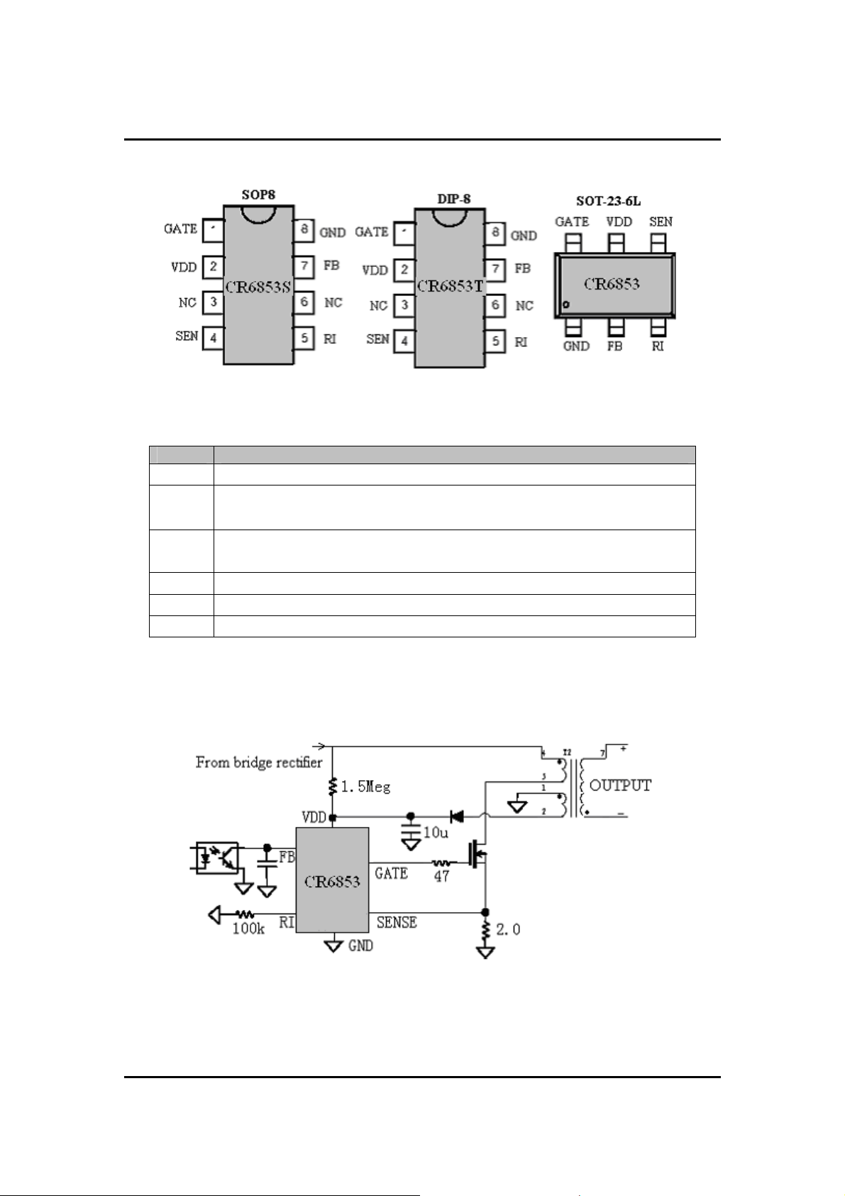
Pin Assignment
Pin Descriptions
Name Description
GND GND Pin
Voltage feedback pin. Output current of this pin could controls the PWM
FB
duty cycle、OLP and SCP.
RI
SEN
VDD
GATE
This pin is to program the switching frequency. By connecting a resistor
to ground to set the switching frequency.
Current sense pin, a resistor connects to sense the MOSFET current.
Supply voltage pin.
Totem output to drive the external power MOSFET.
TYPICAL APPLICATION
Dec, 2007 V1.1 2/11
Chengdu Chip-Rail Tech. Co., Ltd. http://www.chiprail.com
Page 3
8 (10S)
CR6853
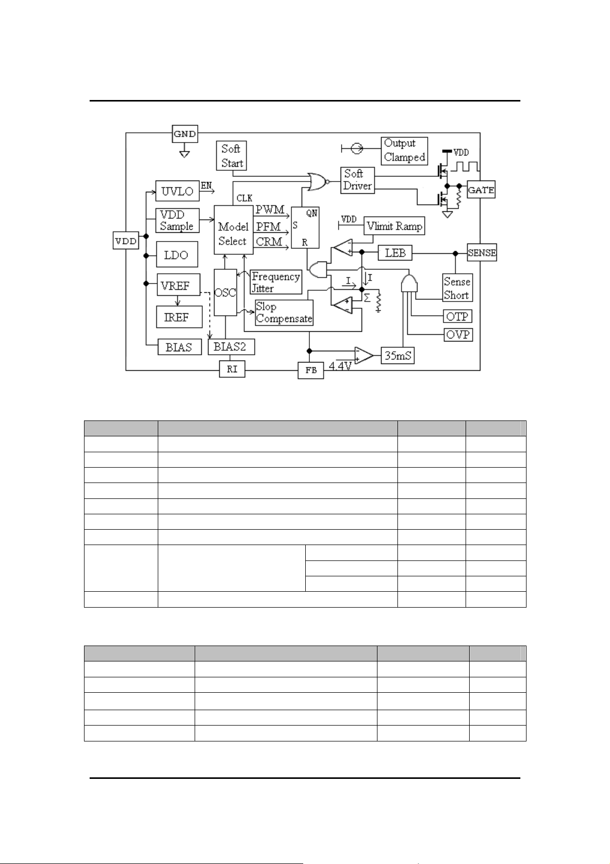
Block Diagram
Simplified Internal Circuit Architecture
Absolute Maximum Ratings
Symbol Parameter Rating Unit
V
DD
I
OVP
V
FB
V
SEN
P
D
T
L
T
STG
Supply voltage Pin Voltage 40 V
VDD OVP maximal enter current 20 mA
Input Voltage to FB Pin -0.3 to 6V V
Input Voltage to SEN Pin -0.3 to 6V V
Power Dissipation 300 mW
ESD Capability, HBM Model 2500 V
ESD Capability, Machine Model 250 V
Lead Temperature
(Soldering)
Storage Temperature Range -55 to + 150
SOT-23-6L (20S)
DIPSOP-8 (10S)
220
260
230
℃
℃
℃
℃
RECOMMENDED OPERATION CONDITION
Symbol Parameter Min ~ Max Unit
VDD VDD Supply Voltage 10~30 V
RI RI PIN Resistor Value 100 K ohm
TOA Operation Ambient Temperature -20~85
P
Maximal Output Power 0~80 W
OMAX
F
PWM
Frequency of PWM 30~150 kHz
℃
Dec, 2007 V1.1 3/11
Chengdu Chip-Rail Tech. Co., Ltd. http://www.chiprail.com
Page 4

CR6853
Electrical Characteristics
Symbol
Supply Voltage (VDD Pin)
VDD
VDD
VDD
I
ST
I
SS
ON
OFF
CLAMP
Startup Current 3.0 20.0
Operating Current
Turn-on Threshold Voltage 13.0 14.0 15.0 V
Turn-off Threshold Voltage 7.8 8.8 9.8 V
VDD Clamp Voltage I
Anti Intermission Surge
VDD
AIS
VDD Voltage
T
OFF
T
RESTART
Over temperature Protection 130
Temperature restart 100
Parameter Conditions Min. Typ. Max. Unit
(Ta=25°C unless otherwise noted, VDD = 15V)
VFB=0V 3.0
VFB=3V 1.4
VFB=Open 1.0
=10mA 34.0
VDD
12.7
µA
mA
mA
mA
V
V
℃
℃
Voltage Feedback (FB Pin)
IFB Short Circuit Current VFB=0V 1.2
VFB Open Loop Voltage VFB=Open 4.8
I
Zero Duty Cycle FB current 1.47
FB_0D
I
PFM
I
CRM
V
PFM
V
CRM
I
OLP&SCP
V
OLP&SCP
T
OLP&SCP
Enter PFM FB current 1.37
Enter CRM FB current 1.45
Enter PFM Threshold V
FB
0.51
Enter CRM Threshold VFB 0.30
Enter OLP&SCP FB current 152
Enter OLP&SCP FB voltage 3.7
OLP&SCP min. delay Time RI=100K 33 35 50 mS
Current Sensing (SEN Pin)
SEN Minimum Voltage Level RI=100K,
V
TH_L
0.70
FB=3.3V
mA
V
mA
mA
mA
V
V
uA
V
V
V
TH_H
0.80
V
FB=3.3V
TPD Delay to Output FB=3.3V 75 ns
SEN Maximum Voltage Level RI=100K,
RCS Input Impedance
V
SCP
Dec, 2007 V1.1 4/11
Sense short protect voltage 177
40 KΩ
mV
Chengdu Chip-Rail Tech. Co., Ltd. http://www.chiprail.com
Page 5

CR6853
T
LEB
( LEB )
Oscillator (RI Pin)
Leading edge blanking time
F
Normal Frequency RI=100Kohm 60 65 70 KHz
OSC
F
PFM Frequency RI=100Kohm 22 KHZ
PFM
DC
DC
ΔF
T
F
MAX_W
MAX_F
TEMP
BLANK
JITTER
Maximum Duty Cycle PWM RI=100Kohm 77 %
Maximum Duty Cycle PFM RI=100Kohm 14 %
Frequency Temp. Stability
Leading-Edge Blanking Time 300
Frequency jitter RI=100Kohm -4 4 %
GATE Drive Output (GATE Pin)
Output Low Level VDD=16V,
V
OL
Output High Level VDD=16V,
V
OH
RI=100K 300
-30-100℃
5 %
0.8 V
IO=20mA
10 V
IO=20mA
nS
nS
VG
T
R1
T
F1
T
R2
T
F2
T
R3
T
F3
T
R4
T
F4
CLAMP
Rising Time
Falling Time CL=500pF 71 ns
Rising Time
Falling Time CL=1000pF 116
Rising Time
Falling Time CL=1500pF 153
Rising Time
Falling Time CL=2000pF 209
Output Clamp Voltage VDD=20V 18.0
Low EMI technique
f
EMI
Low EMI frequency RI=100Kohm 64 Hz
Frequency modulation range
∆f_osc
/Base frequency
CL=500pF 123
CL=1000pF 248 ns
ns
ns
CL=1500pF 343 ns
ns
CL=2000pF 508 ns
ns
V
RI=100Kohm -3 3 %
Dec, 2007 V1.1 5/11
Chengdu Chip-Rail Tech. Co., Ltd. http://www.chiprail.com
Page 6

CR6853
OPERATION DESCRIPTION
Current Mode
Compared to voltage mode control,
current mode control has a current feedback
loop. When the voltage of the Sense resistor
peak current of the primary winding reaches
the internal setting value VTH, the register
resets and the power MOSFET cuts off. So,
to detect and modulate the peak current
cycle-by-cycle could control the output of the
power supply. The current feedback has a
good linear modulation rate and a fast input
and output dynamic impact, and avoid the
pole that the output filter inductance brings
and the two-class system descends to the
one-class. So it widens the frequency range
and optimizes overload protection and short
circuit protection.
Startup Current and Under Voltage
Lockout
The startup current of CR6853 is set to
be very low so that a large value startup
resistor can be used to minimize the power
loss. For AC to DC adaptor with universal
input range design, a 2 MΩ, 1/8 W startup
resistor and a 10uF/25V VDD hold capacitor
could be used.
The turn-on and turn-off threshold of the
CR6853 is designed to 12.8V/7.8V. During
startup, the hold-up capacitor must be
charge to 13.0V through the startup resistor.
The hysteresis is implemented to prevent
the shutdown from the voltage dip during
startup.
Internal Bias and OSC Operation
A resistor connected between RI pin
and GND pin sets the internal constant
current source to charge or discharge the
internal fixed capacitor. The charge time and
discharge time determines the internal clock
speed and the switching frequency.
Increasing the resistance will reduce the
value of the input current and reduce the
switching frequency. The relationship
between RI and PWM switching frequency
follows the below equation within the RI
allowed range.
F
OSC
For example, a 100kΩ resistor RI could
6500
=
)(
KRI
Ω
kHz
)(
generate a 13uA constant current and a
65kHz PWM switching frequency. The
suggested operating frequency range of
CR6853 is within 30KHz to 150KHz.
Green Power Operation
The power dissipation of switching
mode power supply is very important in zero
load or light load condition. The major
dissipation results from conduction loss、
switching loss and consume of the control
circuit. However, all of them relates to the
switching frequency. There are many
difference topologies has been implemented
in different chip. The basic operation theory
of all these approaches intends to reduce
the switching frequency under light-load or
no-load condition.
The CR6853`s green power function
adapts PWM、PFM and CRM combining
modulation. When RI resistor is 100kΩ, the
PWM frequency is 65kHz in medium or
heavy load operation. Through modifying
the pulse width, The CR6853 could control
output voltage. The current of FB pin
increases when the load is in light condition
and the internal mode controller enters
PFM&PWM when the feedback current is
over 1.0mA. The operation frequency of
oscillator is to descend gradually. When the
feedback current is over 1.40mA, the
frequency of oscillator is invariable, namely
22kHz.
CR6853 Green-Power Function
To decrease the standby consumption
of the power supply, Chip-Rail introduces
the Cycle Reset Mode technology (CRM). If
the feedback current is over 1.45mA, mode
controller of the CR6853 would reset
internal register all the time and cut off the
GATE pin. While the output voltage is lower
than the set value, the register would be set,
Dec, 2007 V1.1 6/11
Chengdu Chip-Rail Tech. Co., Ltd. http://www.chiprail.com
Page 7

2
CR6853
the GATE pin operate again. So the
frequency of the internal OSC is invariable,
the register would reset some pulses so that
the practical frequency is decreased at the
GATE pin.
Internal Synchronized Slop
Compensation
Although there are more advantages of
the current mode control than conventional
voltage mode control, there are still several
drawbacks of peak-sensing current-mode
converter, especially the open loop
instability when it operates in higher than
50% of the duty-cycle. To solve this problem,
the CR6853 is introduced an internal slope
compensation adding voltage ramp to the
current sense input voltage for PWM
generation. It improves the close loop
stability greatly at CCM, prevents the
sub-harmonic oscillation and thus reduces
the output ripple voltage.
V
SLOP
DUTY
DUTY
MAX
DUTY
×=×= 4389.033.0
V
value (
IN
I ×=∆
T
) due to the system
L
D
P
delay time that is from detecting the current
through the Sense pin to power MOSFET off
in the CR6853 (Among these, V
is the
IN
primary winding voltage of the transformer
and LP is the primary wind inductance). V
IN
ranges from 85VAC to 264VAC. To
guarantee the output power is a constant for
universal input AC voltage, there is a
dynamic peak limit circuit to compensate the
system delay T that the system delay brings
on.
IPEAK
IPEAK
MAX
MAX
R
R
V
SENSE
85.0
SENSE
==
IN
V
==
IN
)264(
VV
)85(
VV
65.0
Low EMI technique
The frequency low EMI technique is
introduced in the CR6853. As following
figure, the internal oscillation frequency is
modulated by itself. A whole surge cycle
includes 8 pulses and the jittering ranges
from -4% to +4%. Thus, the function could
minimize the electromagnetic interferer from
the power supply module.
Slop Compensation
Current Sensing & Dynamic peak
limiting
MOSFET comes into being a voltage V
on the Sense pin cycle-by-cycle, which
compares to the internal reference voltage,
and controls the reverse of the internal
register, limits the peak current IMAX of the
primary of the transformer. The transformer
energy is
the R
power of the power supple. The current
flowing by the power MOSFET has an extra
Dec, 2007 V1.1 7/11
The current flowing by the power
SENSE
1
can set the maximal output
SENSE
2
. So adjusting
ILE ××=
MAX
OLP&SCP
To protect the circuit from being
damaged under the over load or short circuit
condition, a smart OLP&SCP function is
implemented in the CR6853. When short
circuit or over load occurs in the output end,
the feedback cycle would enhance the
voltage of FB pin, while the voltage is over
4.2V or the current from FB is below 152uA,
the internal detective circuit would send a
signal to shut down the GATE and pull down
the VDD voltage, then the circuit is restart.
To avoid the wrong operation when circuit
starts, the delay time is set. When the RI
Frequency low EMI
Chengdu Chip-Rail Tech. Co., Ltd. http://www.chiprail.com
Page 8

10
6
10
6
×
×
×
×
CR6853
resistance is 100Kohm, the delay time
T
OLP&SCP
relationship between RI and T
follows the below equation.
is between 33mS and 50mS. The
RI
2
)(
TmS
3
&
RI
<<
SCPOLP
OLP&SCP
3
3
mS
)(
Over Temperature Protection
The CR6853 has a built-in temperature
sensing circuit to shut down PWM output
once the junction temperature exceeds
130°C. While PWM output is shut down,
VDD voltage will gradually drop to the UVLO
voltage, and VDD voltage will gradually
increase again. If the junction temperature is
still higher than 130°C, the PWM controller
will be shut down again. This situation will
continue until the temperature drops below
100°C. The PWM output will then be turned
back. The temperature hysteresis window
for the OTP circuit is 30°C.
Sense Fault Detect
Changing the resistance of Sense pin
could limit the maximal peak current of
power MOSFET. If the Sense pin is short
circuit to the ground and the CR6853 is
overload, the power MOSFET and
transformer is easy to be shattered. So, the
short circuit protection is built in the CR6853.
Every time to start up, the circuit would
detect the voltage of the Sense pin when the
start signal is send. If the voltage keeps
lower than 177mV, the circuit would be cut
off and restart in 1.2mS. But, when the
switch power is cut off, there could always
be a big noise on the ground, so to achieve
this function, it is strongly suggested that the
board on the ground of the sense pin must
be attention.
Anti Intermission Surge
When the power supplies change the
heavy load to light load immediately, there
could be tow phenomena caused by system
delay. They are output voltage overshot and
intermission surge. To avoid it, the anti
intermission surge is built in the CR6853. If it
occurs, the FB current is to increase rapidly,
the GATE would be cut off for a while, VDD
pin voltage descends gradually. When VDD
reaches 12.7V, the GATE pin would operate
again, which the frequency is 22KHz and
the max. Duty cycle is 14%.
Leading-edge Blanking (LEB)
Each time the power MOSFET is
switched on, a turn-on spike will inevitably
occur at the Sense pin, which would disturb
the internal signal from the sampling of the
R
blanking time built in to avoid the effect of
the turn-on spike, and the power MOSFET
cannot be switched off during the moment.
So that the conventional external RC
filtering on sense input is no longer required.
. There is a 300nS leading edge
SENSE
Over Voltage Protection (OVP)
There is a 25.6V over-voltage
protection circuit in the CR6853 to improve
the credibility and extend the life of the chip.
When the VDD voltage is over 25.6V, the
GATE pin is to shutdown immediately and
the VDD voltage is to descend rapidly.
GATE Driver & Soft Clamped
The CR6853’ output designs a totem
pole to drive a periphery power MOSFET.
The dead time is introduced to minimize the
transfixion current during the output
operating. The novel soft clamp technology
is introduced to protect the periphery power
MOSFET from breaking down and current
saturation of the Zener.
Dec, 2007 V1.1 8/11
Chengdu Chip-Rail Tech. Co., Ltd. http://www.chiprail.com
Page 9

CR6853
PACKAGE DEMENSIONS
DIP-8L
Dimensions
Symbol
Min. Typ. Max. Min. Typ. Max.
A
A1 0.381
A2 3.175 3.302 3.429 0.125 0.130 0.135
b
b1
D 9.017 9.271 10.160 0.355 0.365 0.400
E
E1 6.223 6.350 6.477 0.245 0.250 0.255
e
L 2.921 3.302 3.810 0.115 0.130 0.150
eB 8.509 9.017 9.525 0.335 0.355 0.375
θ˚ 0˚ 7˚ 15˚ 0˚ 7˚ 15˚
Dec, 2007 V1.1 9/11
Millimeters
1.524
0.457
7.620
2.540
Chengdu Chip-Rail Tech. Co., Ltd. http://www.chiprail.com
5.334
0.015
Inches
0.060
0.018
0.300
0.100
0.210
Page 10

CR6853
SOT-23-6L
Symbol
Dimensions In Millimeters
Min Max Min Max
A 0.700 1.000 0.028 0.039
A1 0.000 0.100 0.000 0.004
B 1.397 1.803 0.055 0.071
b 0.300 0.559 0.012 0.022
C 2.591 3.000 0.102 0.118
D 2.692 3.099 0.106 0.122
e 0.838 1.041 0.033 0.041
H 0.080 0.254 0.003 0.010
L 0.300 0.610 0.012 0.024
Dimensions In Inches
Dec, 2007 V1.1 10/11
Chengdu Chip-Rail Tech. Co., Ltd. http://www.chiprail.com
Page 11

CR6853
SOP-8L
Dimensions DISCLAIMERS
Millimeter
0.381X45
Symbol
A 1.346
A1 0.101
b
c
D 4.648
E 3.810
e 1.016 1.270 1.524 0.040 0.050 0.060
F
H 5.791
L 0.406
θ˚
Min. Typ. Max. Min. Typ. Max.
0°
0.406
0.203
°
1.752 0.053
0.254 0.004
4.978 0.183
3.987 0.150
6.197 0.228
1.270 0.016
8° 0°
Inch
0.016
0.008
0.015X45
°
0.069
0.010
0.196
0.157
0.244
0.050
8°
Dec, 2007 V1.1 11/11
Chengdu Chip-Rail Tech. Co., Ltd. http://www.chiprail.com
Page 12

 Loading...