

Page 1

Automotive Thick Film Chip Resistors - CQ
Feature
• Tolerance: ±0.5%~±5%
• Application automobile industry, comply with the relevant provisions of AEC-Q200.
• Anti-sulfurized performance: H
• Resistance range: 1Ω~10MΩ,0 Ω
• Operating temperature range: -55°C ~+155°C
• Stable electrical capability, high reliability
• Suit for reflow & wave soldering
• RoHS complaint
2
S 3~5ppm, 50°C±2°C, 91%~93%RH, 1000H
Application
Derating Curve
• Intelligent home appliances
• High-end computer
• Medical equpment
• Industrial equpment
• Outdoor electronic application
Percent rated load (%)
Ambient temperature (°C)
Figures
L
A
H
L
W
W
B
H
1. High purity Alumina substrate
2. Protective coating
3. Resistance element
4. Termination (Inner) Ni / Cr
5. Termination (Between) Ni Barrier
6. Termination (Outer) Sn
Dimension (mm)
TYype L W H A B
CQ01 (0201) 0.60±0.03 0.30±0.03 0.23±0.03 0.12±0.05 0.15±0.05
CQ02 (0402) 1.00±0.10 0.50±0.05 0.35±0.05 0.20±0.10 0.25±0.10
CQ03 (0603) 1.60±0.10 0.80±0.10 0.45±0.10 0.30±0.20 0.30±0.20
CQ05 (0805) 2.00±0.15 1.25
CQ06 (1206) 3.10±0.15 1.55
CQ07 (1210) 3.10±0.10 2.60±0.20 0.55±0.10 0.50±0.25 0.50±0.20
CQ10 (2010) 5.00±0.10 2.50±0.20 0.55±0.10 0.60±0.25 0.50±0.20
CQ12 (2512) 6.35±0.10 3.20±0.20 0.55±0.10 0.60±0.25 0.50±0.20
+0.15
-0.10
+0.15
-0.10
0.55±0.10 0.40±020 0.40±0.20
0.55±0.10 0.45±020 0.45±0.20
Specification
Type
CQ01(0201) 1/20W
CQ02(0402) 1/16W 50V 100V 100V <50mΩ 1A 2A
CQ03(0603) 1/10W 75V 150V 300V <50mΩ 1A 2A
CQ05(0805) 1/8W 150V 300V 500V <50mΩ 2A 5A
CQ06(1206) 1/4W 200V 400V 500V <50mΩ 2A 10A
CQ07(1210) 1/2W 200V 500V 500V <50mΩ 2A 10A
CQ10(2010) 3/4W 200V 500V 500V <50mΩ 2A 10A
CQ12(2512) 1W 200V 500V 500V <50mΩ 2A 10A
40
Power
(70°C)
Tolerance
±0.5%
±1%
±2%
±5%
Resistance
Range
0 Ω
1Ω~10MΩ
Max Working
Voltage
25V 50V / <50mΩ 0.5A 1A
Max Overload
Voltage
Dielectric
With-standing
Voltage
Resistance
Value of Jumper
Rated Current of
Jumper
Max. Current of
Jumper
Operating
Temperature
Range
-55~+155°C
Page 2
Automotive Thick Film Chip Resistors - CQ
Performance Specification
Test Item Reference standard Test Methods Evaluation Criteria
Temperature Coefficient
of Resistance
Pre- and Post-Stress
ElectricalTest
(Short time Overload)
Biased Humidity AEC-Q200 TEST 7
Operational Life AEC-Q200 TEST 8
Resistance to Soldering
Solderability AEC-Q200 TEST 18
Board Flex AEC-Q200 TEST 21
Sulfuration test H
MIL-STD-202 Method 304 Measure between: -55°C ~+155°C CQ01: 1Ω≤R≤10Ω: -100~+350ppm/°C
AEC-Q200 TEST 1
IEC60115 4.13
MIL-STD-202 Method 103
MIL-STD-202 Method 108
AEC-Q200 TEST 15
Heat
MIL-STD-202 Method 210
J-STD-002
AEC-Q200-005
>10Ω: ±200ppm/°C
CQ02-CQ12:
1Ω≤R≤10Ω: ±200ppm/°C
>10Ω: ±100ppm/°C
2.5x Rated voltage or Max. Overload Voltage whichever is lower for 5 seconds,
then check the resistance.
1000 hours 85°C/85%RH. Note: Specified conditions:10% of operating power.
Measurement at 24±4 hours after test conclusion.
1,000 hours at 125°C, applied de-rated (36%) power of continuous working
voltage, 1.5 hours on, 0.5 hour off.
Condition B No pre-heat of samples. Note: Single Wave Solder - Procedure 2 for
SMD and Procedure 1 for Leaded with solder within 1.5mm of device body.
SMD. Electrical test not required. Magnification 50 X.
Conditions:
1. Baking 4 hours@155°C dry heat, dipping @ 245±3°C for 5±0.5 second.
2. Steam aging 8 hours, dipping @ 260±3°C for 30±0.5 second.
Bending 3mm(CQ01-CQ05)/2mm(CQ06-CQ12)for 60±5sec ±(1.0%+0.05Ω
2
S 3~5PPM 50°C±2°C 91%~93% RH 1000H
±1%: ±(1.0%+0.05Ω)
±5%: ±(2.0%+0.05Ω)
±1%: ±(1.0%+0.05Ω)
±5%: ±(3.0%+0.05Ω)
±1%: ±(1.0%+0.1Ω)
±5%: ±(3.0%+0.1Ω)
±(1.0%+0.05Ω)
Coverage must be over 95%.
±5%: ±(5.0%+0.05 Ω)
±1%: ±(1.0%+0.05 Ω)
)
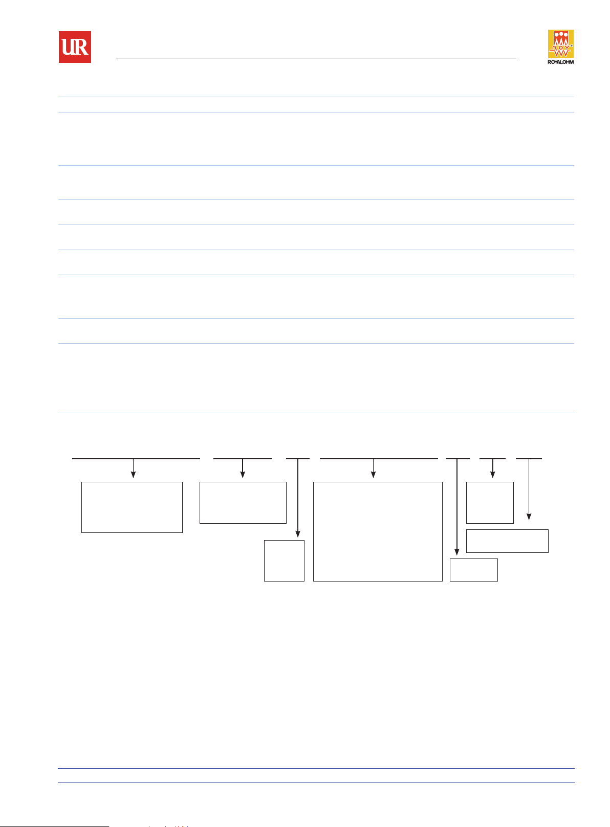
Ordering Procedure (Example: CQ06 1/4W 5% 1.2 Ω T/R-5000)
CQ06 W4 J 012JT 5 E
Packing Type:
T = T/R
Packing Qty.:
4=4,000pcs
5=5,000pcs
C=10,000pcs
Special Feature:
E = Lead Free (standard)
Produc t Type:
Fill-in 4 digits with the Chip
resistor type as follow
CQ02, CQ03, CQ05, CQ06, CQ07,
CQ10 , CQ12
:
Watta ge:
Fill-in 2 digits with the
codes as follow:
WG = 1/16W WA = 1/10W
Tolerance :
F = ±1%
G = ±2%
J = ±5%
Resistance Value:
2%, 5%(E-24 series):
st
digit is “0”, the 2nd & 3rd digits are for
the 1
the significant figures of the resistance
th
and the 4
following
≤1%(E-96 series):
the 1
figures of the resistance and the 4
indicate the numbers of zeros following
indicate the numbers of zeros
st
to 3rd digits are for the significant
th
Remark: For more details, please check page 135, Part No. System
41
 Loading...