

Page 1

TL/DD12065
COP888GW 8-Bit Microcontroller with Pulse Train Generators and Capture Modules
PRELIMINARY
September 1996
COP888GW
8-Bit Microcontroller with Pulse Train Generators
and Capture Modules
General Description
The COP888 family of microcontrollers uses an 8-bit single
chip core architecture fabricated with National Semiconductor’s M
2
CMOSTMprocess technology. The COP888GW is a
member of this expandable 8-bit core processor family of
microcontrollers. It is a fully static part, fabricated using double-metal silicon gate microCMOS technology.
Features include an 8-bit memory mapped architecture, MICROWIRE/PLUS serial I/O, two 16-bit timer/counters supporting three modes (Processor Independent PWM generation, External Event counter and Input Capture mode capabilities), four independent 16-bit pulse train generators with
16-bit prescalers, two independent 16-bit input capture
modules with 8-bit prescalers, multiply and divide functions,
full duplex UART, and two power savings modes (HALT and
IDLE), both with a multi-sourced wake up/interrupt capability. This multi-sourced interrupt capability may also be used
independent of the HALT or IDLE modes.
Each I/O pin has software selectable configurations. The
devices operate over a voltage range of 2.5V –6V. High
throughput is achieved with an efficient, regular instruction
set operating at a maximum of 1 ms per instruction rate. The
device has low EMI emissions. Low radiated emissions are
achieved by gradual turn-on output drivers and internal I
CC
filters on the chip logic and crystal oscillator. The device is
available in 68-pin PLCC package.
Key Features
Y
Two 16-bit input capture modules with 8-bit prescalers
Y
Four Pulse Train Generators with 16-bit prescalers
Y
Full duplex UART
Y
Two 16-bit timers, each with two 16-bit registers
supporting:
Ð Processor independent PWM mode
Ð External event counter mode
Ð Input capture mode
Y
Quiet design (low radiated emissions)
Y
16 kbytes on-board ROM
Y
512 bytes on-board RAM
Additional Peripheral Features
Y
Idle Timer
Y
Multi-Input Wake-Up (MIWU) with optional interrupts (8)
Y
MICROWIRE/PLUSTMserial I/O
I/O Features
Y
Memory mapped I/O
Y
Software selectable I/O options (TRI-STATEÉOutput,
Push-Pull Output, Weak Pull-Up Input, High Impedance
Input)
Y
Schmitt trigger inputs on port G
Y
Package: 68-pin PLCC
CPU/Instruction Set Features
Y
1 ms instruction cycle time
Y
Fourteen multi-source vectored interrupts servicing:
Ð External Interrupt with selectable edge
Ð Idle Timer T0
Ð Two Timers (each with 2 interrupts)
Ð MICROWIRE/PLUS
Ð Multi-Input Wake-Up
Ð Software Trap
Ð UART (2)
Ð Capture Timers
Ð Counters (one vector for all four counters)
Ð Default VIS (default interrupt)
Y
Versatile and easy-to-use instruction set
Y
8-bit Stack Pointer SPÐ(stack in RAM)
Y
Two 8-bit register indirect data memory pointers
(B and X)
Fully Static CMOS
Y
Two power saving modes: HALT and IDLE
Y
Low current drain (typicallyk1 mA)
Y
Single supply operation: 2.5V –5.5V
Y
Temperature range:b40§Ctoa85§C
Development Support
Y
Emulation and OTP device
Y
Real time emulation and full program debug offered by
MetaLink’s Development System
TRI-STATEÉis a registered trademark of National Semiconductor Corporation.
M
2
CMOSTM, MICROWIRE/PLUSTM, COPSTM, MICROWIRETMand WATCHDOGTMare trademarks of National Semiconductor Corporation.
IBM
É
,PCÉ, PC-ATÉand PC/XTÉare registered trademarks of International Business Machines Corporation.
iceMASTER
TM
is a trademark of MetaLink Corporation.
C
1996 National Semiconductor Corporation RRD-B30M106/Printed in U. S. A.
http://www.national.com
Page 2
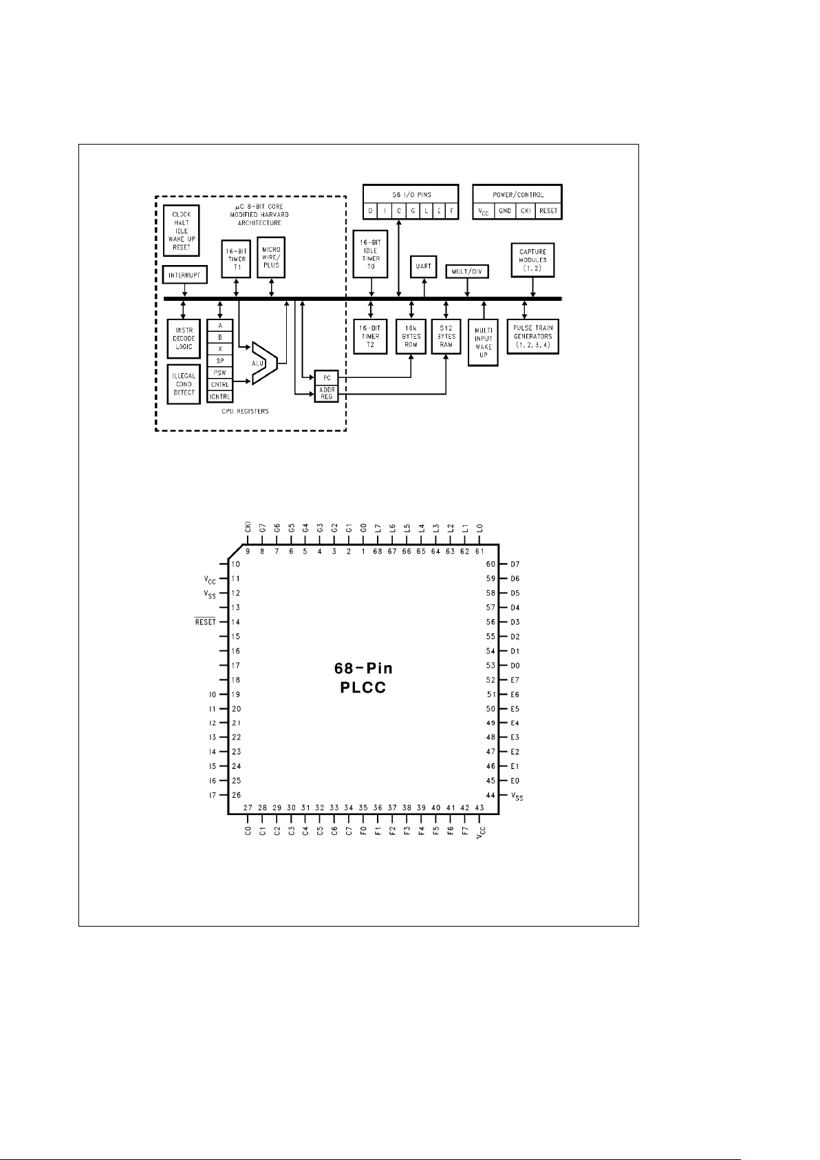
Block Diagram
TL/DD/12065– 1
FIGURE 1. COP888GW Block Diagram
Connection Diagram
TL/DD/12065– 2
Top View
Order Number COP888GW-XXX/V
See NS Package Number V68A
http://www.national.com 2
Page 3
Absolute Maximum Ratings (Note)
SuppIy Voltage (V
CC
)7V
Voltage at Any Pin
b
0.3V to V
CC
a
0.3V
Total Current into VCCPin (Source) 100 mA
Total Current out of GND Pin (Sink) 110 mA
Storage Temperature Range
b
65§Ctoa150§C
Note:
Absolute maximum ratings indicate limits beyond
which damage to the device may occur. DC and AC electrical specifications are not ensured when operating the device at absolute maximum ratings.
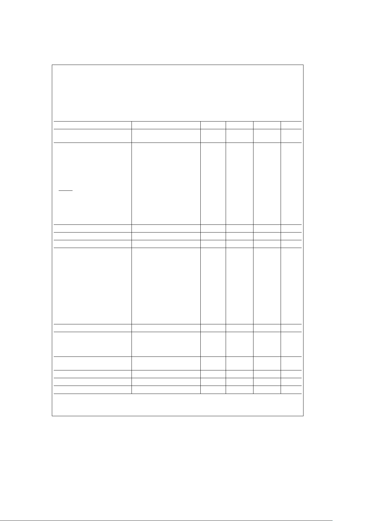
DC Electrical Characteristics COP888GW:
b
40§CsT
A
s
a
85§C unless otherwise specified
Parameter ConditIons Min Typ Max UnIts
Operating Voltage 2.5 6.0 V
Power Supply Ripple (Note 1) Peak-to-Peak 0.1 V
CC
V
Supply Current (Note 2)
CKI
e
10 MHz V
CC
e
6V, t
c
e
1 ms10mA
CKI
e
4 MHz V
CC
e
2.5V, t
c
e
2.5 ms 1.7 mA
HALT Current (Note 3) V
CC
e
6V, CKIe0 MHz
k
110mA
IDLE Current
CKI
e
10 MHz V
CC
e
6V 1.7 mA
CKI
e
4 MHz V
CC
e
2.5V 0.4 mA
Input Levels (V
IH,VIL
)
RESET
, CKI
Logic High 0.8 V
CC
V
Logic Low 0.2 V
CC
V
All Other Inputs
Logic High 0.7 V
CC
V
Logic Low 0.2 V
CC
V
Hi-Z Input Leakage V
CC
e
6V
b
2
a
2 mA
Input Pullup Current V
CC
e
6V, V
IN
e
0V
b
40
b
250 mA
G Port Input Hysteresis (Note 6) 0.05 V
CC
0.35 V
CC
V
Output Current Levels
D Outputs
Source V
CC
e
4V, V
OH
e
3.3V
b
0.4 mA
V
CC
e
2.5V, V
OH
e
1.8V
b
0.2 mA
Sink V
CC
e
4V, V
OL
e
1V 10 mA
V
CC
e
2.5V, V
OL
e
0.4V 2.0 mA
All Others
Source (Weak Pull-Up Mode) V
CC
e
4V, V
OH
e
2.7V
b
10
b
100 mA
V
CC
e
2.5V, V
OH
e
1.8V
b
2.5
b
33 mA
Source (Push-Pull Mode) V
CC
e
4V, V
OH
e
3.3V
b
0.4 mA
V
CC
e
2.5V, V
OH
e
1.8V
b
0.2 mA
Sink (Push-Pull Mode) V
CC
e
4V, V
OL
e
0.4V 1.6 mA
V
CC
e
2.5V, V
OL
e
0.4V 0.7 mA
TRI-STATE Leakage V
CC
e
6.0V
b
2
a
2 mA
Allowable Sink/Source
Current per Pin
D Outputs (Sink) 15 mA
All others 3mA
Maximum Input Current Room Temp
g
200 mA
without Latchup (Note 4, 6)
RAM Retention Voltage, VR(Note 5) 500 ns Rise and Fall Time (min) 2 V
Input Capacitance (Note 6) 7 pF
Load Capacitance on D2 (Note 6) 1000 pF
http://www.national.com3
Page 4
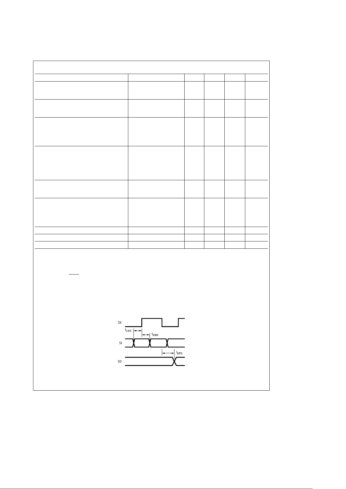
AC Electrical Characteristics COP888GW:
b
40§CsT
A
s
a
85§C unless otherwise specified
Parameter Conditions Min Typ Max Units
Instruction Cycle Time (tc)
Crystal, Resonator 2.5V
s
V
CC
k
4V 2.5 DC ms
Ceramic V
CC
t
4V 1.0 DC ms
CKI Clock Duty Cycle (Note 5) feMax 40 60 %
Rise Time (Note 5) f
e
10 MHz Ext Clock 5 ms
Fall Time (Note 5) fe10 MHz Ext Clock 5 ms
Inputs
t
SETUP
V
CC
t
4V 200 ns
2.5V
s
V
CC
k
4V 500 ns
t
HOLD
V
CC
t
4V 60 ns
2.5V
s
V
CC
k
4V 150 ns
Output Propagation Delay (Note 8) R
L
e
2.2k, C
L
e
100 pF
t
PD1,tPD0
SO, SK V
CC
t
4V 0.7 ms
2.5V
s
V
CC
k
4V 1.8 ms
All Others V
CC
t
4V 1 ms
2.5V
s
V
CC
k
4V 2.5 ms
MICROWIRETMSetup Time (t
UWS
) (Note 6) V
CC
t
4V 20 ns
MICROWIRE Hold Time (t
UWH
) (Note 6) V
CC
t
4V 56 ns
MICROWIRE Output Propagation Delay (t
UPD
)V
CC
t
4V 220 ns
Input Pulse Width (Note 7)
Interrupt Input High Time 1 t
c
Interrupt Input Low Time 1 t
c
Timer 1, 2 Input High Time 1 t
c
Timer 1, 2 Input Low Time 1 t
c
Capture Timer High Time 1 CKI
Capture Timer Low Time 1 CKI
Reset Pause Width 1 t
c
Note 1: Maximum rate of voltage change to be defined.
Note 2: Supply current is measured after running 2000 cydes with a square wave CKI input, CKO open, inputs at rails and outputs open.
Note 3: The HALT mode will stop CKI from oscillatng. Test conditions: All inputs tied to V
CC
, L, C, E, F, and G port I/O’s configured as outputs and programmed
low and not driving a load; D outputs programmed low and not driving a load. Parameter refers to HALT mode entered via setting bit 7 of the G Port data register.
Part will pull up CKI during HALT in crystal clock mode.
Note 4: Pins G6 and RESET
are designed with a high voltage input network. These pins allow input voltages greater than VCCand the pins will have sink current to
V
CC
when biased at voltages greater than VCC(the pins do not have source current when biased at a voltage below VCC.) The effective resistance to VCCis 750X
(typical). These two pins will not latch up. The voltage at the pins must be limited to less than 14 volts. WARNING: Voltages in excess of 14 volts will cause damage
to the pins. This warning excludes ESD transients.
Note 5: Condition and parameter valid only for part in HALT mode.
Note 6: Parameter characterized but not tested.
Note 7: t
c
e
Instruction Cycle Time
Note 8: The output propagation delay is referenced to the end of the instruction cycle where the output change occurs.
TL/DD/12065– 3
FIGURE 2. MICROWIRE/PLUS Timing
http://www.national.com 4
Page 5
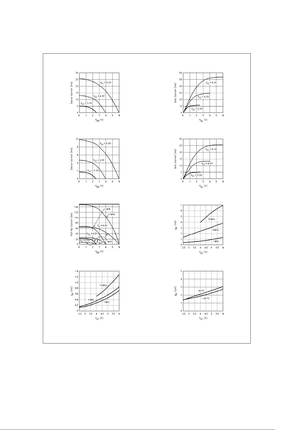
Typical Performance Characteristics
b
40§CsT
A
s
a
85§C
Port D Source Current
TL/DD/12065– 23
Port D Sink Current
TL/DD/12065– 24
Ports C/G/L/E/F Source Current
TL/DD/12065– 25
Ports C/G/L/E/F Sink Current
TL/DD/12065– 26
Ports C/G/L/E/F Weak Pull-Up Source Current
TL/DD/12065– 27
Dynamic Ð IDDvs V
CC
TL/DD/12065– 28
Idle Ð IDDvs V
CC
TL/DD/12065– 29
HALT Ð IDDvs V
CC
TL/DD/12065– 30
http://www.national.com5
Page 6
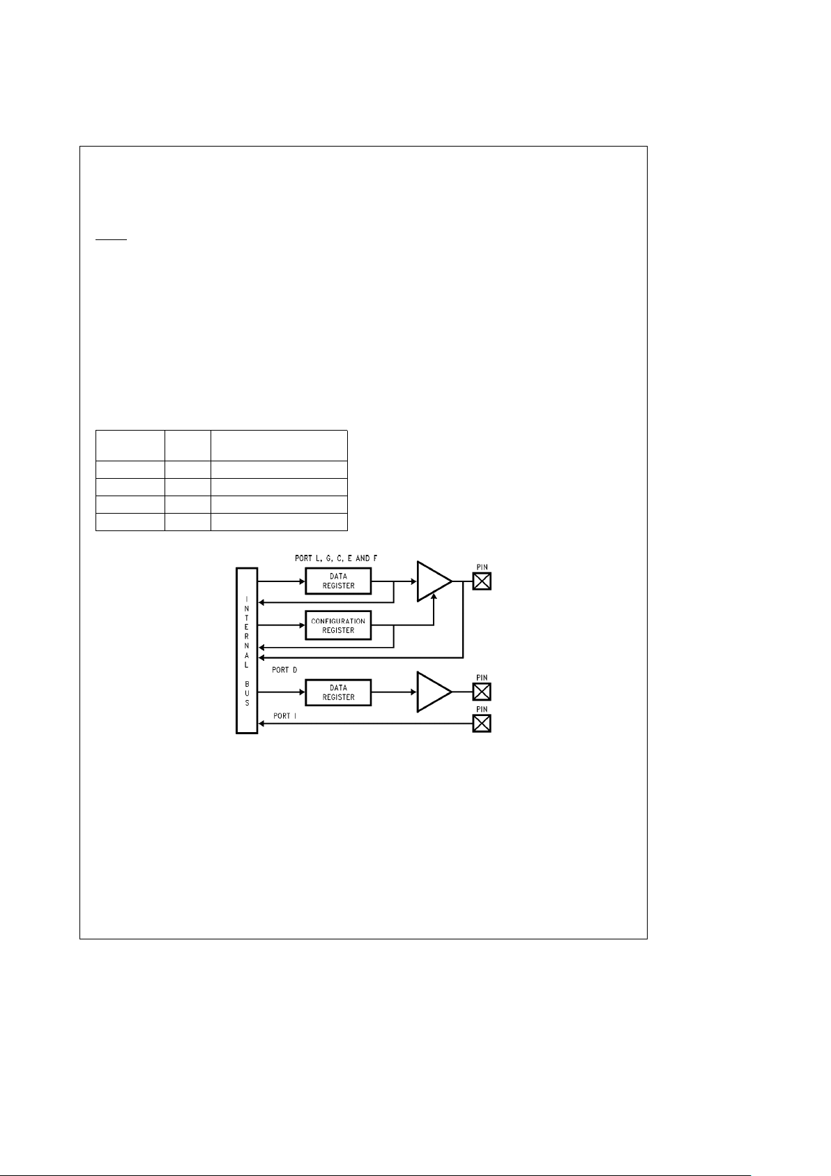
Pin Descriptions
VCCand GND are the power supply pins. All VCCand GND
pins must be connected.
CKI is the clock input. This comes from an R/C generated
oscillator, or a crystal oscillator (in conjunction with CKO).
See Oscillator Description section.
RESET
is the master reset input. See Reset description
section.
The device contains five bidirectional 8-bit I/O ports (C, E,
F, G and L), where each individual bit may be independently
configured as an input (Schmitt trigger inputs on ports L and
G), output or TRI-STATE under program control. Three data
memory address locations are allocated for each of these
I/O ports. Each I/O port has two associated 8-bit memory
mapped registers, the CONFIGURATION register and the
output DATA register. A memory mapped address is also
reserved for the input pins of each I/O port. (See the memory map for the various addresses associated with the I/O
ports.)
Figure 3
shows the I/O port configurations. The
DATA and CONFIGURATION registers allow for each port
bit to be individually configured under software control as
shown below:
Configuration Data
Port Set-Up
Register Register
0 0 Hi-Z Input (TRI-STATE Output)
0 1 Input with Weak Pull-Up
1 0 Push-Pull Zero Output
1 1 Push-Pull One Output
PORT L is an 8-bit I/O port. All L-pins have Schmitt triggers
on the inputs.
The Port L supports Multi-Input Wake Up on all eight pins.
L1 is used for the UART external clock. L2 and L3 are used
for the UART transmit and receive. L4 and L5 are used for
the timer input functions T2A and T2B. L6 and L7 are used
for the capture timer input functions CAP1 and CAP2.
The Port L has the following alternate features:
L0 MIWU
L1 MIWU or CKX
L2 MIWU or TDX
L3 MIWU or RDX
L4 MIWU or T2A
L5 MIWU or T2B
L6 MIWU or CAP1
L7 MIWU or CAP2
Port G is an 8-bit port with 6 I/O pins (G0– G5), an input pin
(G6), and a dedicated output pin (G7). Pins G0– G6 all have
Schmitt Triggers on their inputs. Pin G7 serves as the dedicated output pin for the CKO clock output. There are two
registers associated with the G Port, a data register and a
configuration register. Therefore, each of the 6 I/O bits
(G0–G5) can be individually configured under software control.
TL/DD/12065– 4
FIGURE 3. I/O Port Configurations
http://www.national.com 6
Page 7
Pin Descriptions (Continued)
Since G6 is an input only pin and G7 is dedicated CKO clock
output pin, the associated bits in the data and configuration
registers for G6 and G7 are used for special purpose functions as outlined below. Reading the G6 and G7 data bits
will return zeros.
Note that the chip will be placed in the HALT mode by writing a ‘‘1’’ to bit 7 of the Port G Data Register. Similarly the
chip will be placed in the IDLE mode by writing a ‘‘1’’ to bit 6
of the Port G Data Register.
Writing a ‘‘1’’ to bit 6 of the Port G Configuration Register
enables the MICROWIRE/PLUS to operate with the alternate phase of the SK clock.
Config Reg. Data Reg.
G7 Not Used HALT
G6 Alternate SK IDLE
Port G has the following alternate features:
G0 INTR (ExternaI Interrupt Input)
G2 T1B (Timer T1 Capture Input)
G3 T1A (Timer T1 I/O)
G4 SO (MICROWIRE Serial Data Output)
G5 SK (MICROWIRE SeriaI Clock)
G6 SI (MICROWIRE Serial Data Input)
Port G has the following dedicated functions:
G7 CKO OsciIlator dedicated output
Ports C and F are 8-bit I/O ports.
Port E is an 8-bit I/O port. It has the following alternate
features:
E0 CT1 (Output for counter1, PuIse Train Generator)
E1 CT2 (Output for counter2, Pulse Train Generator)
E2 CT3 (Output for counter3, PuIse Train Generator)
E3 CT4 (Output for counter4, Pulse Train Generator)
Port I is an eight-bit Hi-Z input port.
Port D is an 8-bit output port that is preset high when
RESET
goes Iow. The user can tie two or more D port out-
puts (except D2) together in order to get a higher drive.
Functional Description
The architecture of the device is modified Harvard architecture. With the Harvard architecture, the control store program memory (ROM) is separated from the data store memory (RAM). Both ROM and RAM have their own separate
addressing space with separate address buses. The architecture, though based on Harvard architecture, permits
transfer of data from ROM to RAM.
CPU REGISTERS
The CPU can do an 8-bit addition, subtraction, logical or
shift operation in one instruction (t
c
) cycle time.
There are six CPU registers:
A is the 8-bit Aocumulator Register
PC is the 15-bit Program Counter Register
PU is the upper 7 bits of the program counter (PC)
PL is the lower 8 bits of the program counter (PC)
B is an 8-bit RAM address pointer, which can be optionally
post auto incremented or decremented.
X is an 8-bit alternate RAM address pointer, which can be
optionally post auto incremented or decremented.
SP is the 8-bit stack pointer, which points to the subroutine/
interrupt stack (in RAM). The SP is initialized to RAM address 06F with reset.
S is the 8-bit Data Segment Address Register used to extend the Iower haIf of the address range (00 to 7F) into 256
data segments of 128 bytes each.
All the CPU registers are memory mapped with the exception of the AccumuIator (A) and the Program Counter (PC).
PROGRAM MEMORY
The program memory consists of 16384 bytes of ROM.
These bytes may hoId program instructions or constant data
(data tables for the LAID instruction, jump vectors for the
JID instruction, and interrupt vectors for the VIS instruction).
The program memory is addressed by the 15-bit program
counter (PC). All interrupts in the devices Vector to program
memory location OFF Hex.
DATA MEMORY
The data memory address space includes the on-chip RAM
and data registers, the I/O registers (Configuration, Data
and Pin), the control registers, the MICROWIRE/PLUS SIO
shift register, and the various registers, and counters associated with the timers (with the exception of the IDLE timer).
Data memory is addressed directly by the instruction or indirectly by the B, X, SP pointers and S register.
The data memory consists of 512 bytes of RAM. Sixteen
bytes of RAM are mapped as ‘‘registers’’ at addresses 0F0
to 0FF Hex. These registers can be loaded immediately,
and also decremented and tested with the DRSZ (decrement register and skip if zero) instruction. The memory
pointer registers X, SP, B and S are memory mapped into
this space at address locations 0FC to 0FF Hex respectively, with the other registers being available for general usage.
Note: RAM contents are undefined upon power-up.
Data Memory Segment RAM
Extension
Data memory address 0FF is used as a memory mapped
location for the Data Segment Address Register (S).
The data store memory is either addressed directly by a
single-byte address within the instruction, or indirectly relative to the reference of the B, X, or SP pointers (each contains a single-byte address). This single-byte address allows
an addressing range of 256 locations from 00 to FF hex.
The upper bit of this single-byte address divides the data
store memory into two separate sections as outlined previously. With the exception of the RAM register memory from
address locations 00F0 to 00FF, all RAM memory is memory mapped with the upper bit of the single-byte address being equal to zero. This allows the upper bit of the single-byte
address to determine whether or not the base address
range (from 0000 to 00FF) is extended. If this upper bit
equals one (representing address range 0080 to 00FF),
then address extension does not take place. Alternatively, if
this upper bit equals zero, then the data segment extension
http://www.national.com7
Page 8
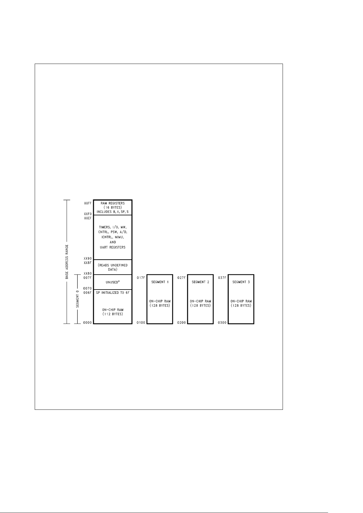
Data Memory Segment RAM Extension (Continued)
register S is used to extend the base address range (from
0000 to 007F) from XX00 to XX7F, where XX represents the
8 bits from the S register. Thus the 128-byte data segment
extensions are located from addresses 0100 to 017F for
data segment 1, 0200 to 027F for data segment 2, etc., up
to FF00 to FF7F for data segment 255. The base address
range from 0000 to 007F represents data segment 0.
Figure 4
illustrates how the S register data memory extension is used in extending the lower half of the base address
range (00 to 7F hex) into 256 data segments of 128 bytes
each, with a total addressing range of 32 kbytes from XX00
to XX7F. This organization allows a total of 256 data segments of 128-bytes each with an additional upper base segment of 128 bytes. Furthermore, all addressing modes are
availabIe for all data segments. The S register must be
changed under program control to move from one data segment (128 bytes) to another. However, the upper base segment (containing the 16 memory registers, I/O registers,
controI registers, etc.) is always available regardless of the
contents of the S register, since the upper base segment
(address range 0080 to 00FF) is independent of data segment extension.
The instructions that utilize the stack pointer (SP) always
reference the stack as part of the base segment (Segment
0), regardless of the contents of the S register. The S register is not changed by these instructions. Consequently, the
stack (used with subroutine linkage and interrupts) is always
located in the base segment. The stack pointer will be initialized to point at data memory location 006F as a result of
reset.
The 128 bytes of RAM contained in the base segment are
split between the Iower and upper base segments. The first
112 bytes of RAM are resident from address 0000 to 006F
in the Iower base segment, while the remaining 16 bytes of
RAM represent the 16 data memory registers located at addresses 00F0 to 00FF of the upper base segment. No RAM
is located at the upper sixteen addresses (0070 to 007F) of
the lower base segment.
Additional RAM beyond these initial 128 bytes, however, will
always be memory mapped in groups of 128 bytes (or less)
at the data segment address extensions (XX00 to XX7F) of
the lower base segment. The additional 384 bytes of RAM
in this device are memory mapped at address locations
0100 to 017F
§
0200 to 027F, and 0300 to 037F hex.
TL/DD/12065– 5
*Reads as all ones.
FIGURE 4. RAM Organization
http://www.national.com 8
Page 9
Reset
This device enters a reset state immediately upon detecting
a logic low on the RESET
pin. The RESET pin must be held
low for a minimum of one instruction cycle to guarantee a
valid reset. During power-up initialization, the user must insure that the RESET
pin is held low until this device is within
the specified V
CC
voltage. An R/C circuit on the RESET pin
with a delay 5 times (5x) greater than the power supply rise
time is recommended.
When the RESET
input goes low, the I/O ports are initialized immediately, with any observed delay being only propagation delay. When the RESET
pin goes high, this device
comes out of the reset state synchronously. This device will
be running within two instruction cycles of the RESET
pin
going high.
RESET
may also be used to exit this device from the HALT
mode.
Some registers are reset to a known state, whereas other
registers and RAM are ‘‘unchanged’’ by reset. When the
controller goes into reset state while it is performing a write
operation to one of these registers or RAM that are ‘‘unchanged’’ by reset, the register or RAM value will become
unknown (i.e. not unchanged). This is because the write operation is terminated prematurely by reset and the results
become uncertain. These registers and RAM locations are
unchanged by reset only if they are not written to when the
controller resets.
The following initializations occur with RESET
:
Port L: TRI-STATE
Port C: TRI-STATE
Port G: TRI-STATE
Port E: TRI-STATE
Port F: TRI-STATE
Port D: HIGH
PC: CLEARED
PSW, CNTRL and ICNTRL registers: CLEARED
SIOR:
UNAFFECTED after RESET with power already applied
RANDOM after RESET at power-on
T1CNTRL: CLEARED
T2CNTRL: CLEARED
TxRA, TxRB: RANDOM
CCMR1, CCMR2: CLEARED
CM1PSC, CM1CRL, CM1CRH, CM2PSC, CM2CRL, and
CM2CRH:
UNAFFECTED after RESET with power already applied
RANDOM after RESET at power-on
CCR1 and CCR2: CLEARED
CxPRH, CxPRL, CxCTH, and CxCTL:
UNAFFECTED after RESET with RC clock option (power
already applied)
RANDOM after RESET at power-on
PSR, ENUR and ENUI: CLEARED
ENU: CLEARED except Bit 1 (TBMT)
e
1
Accumulator, Timer 1 and Timer 2:
RANDOM after RESET with crystal clock option (power already applied)
RANDOM after RESET at power-on
MDCR: CLEARED
MDR1, MDR2, MDR3, MDR4, MDR5: RANDOM
WKEN, WKEDG: CLEARED
WKPND: RANDOM
S Register: CLEARED
SP (Stack Pointer): Loaded with 6F Hex
B and X Pointers:
UNAFFECTED after RESET with power already applied
RANDOM after RESET at power-on
RAM:
UNAFFECTED after RESET with power already applied
RANDOM after RESET at power-on
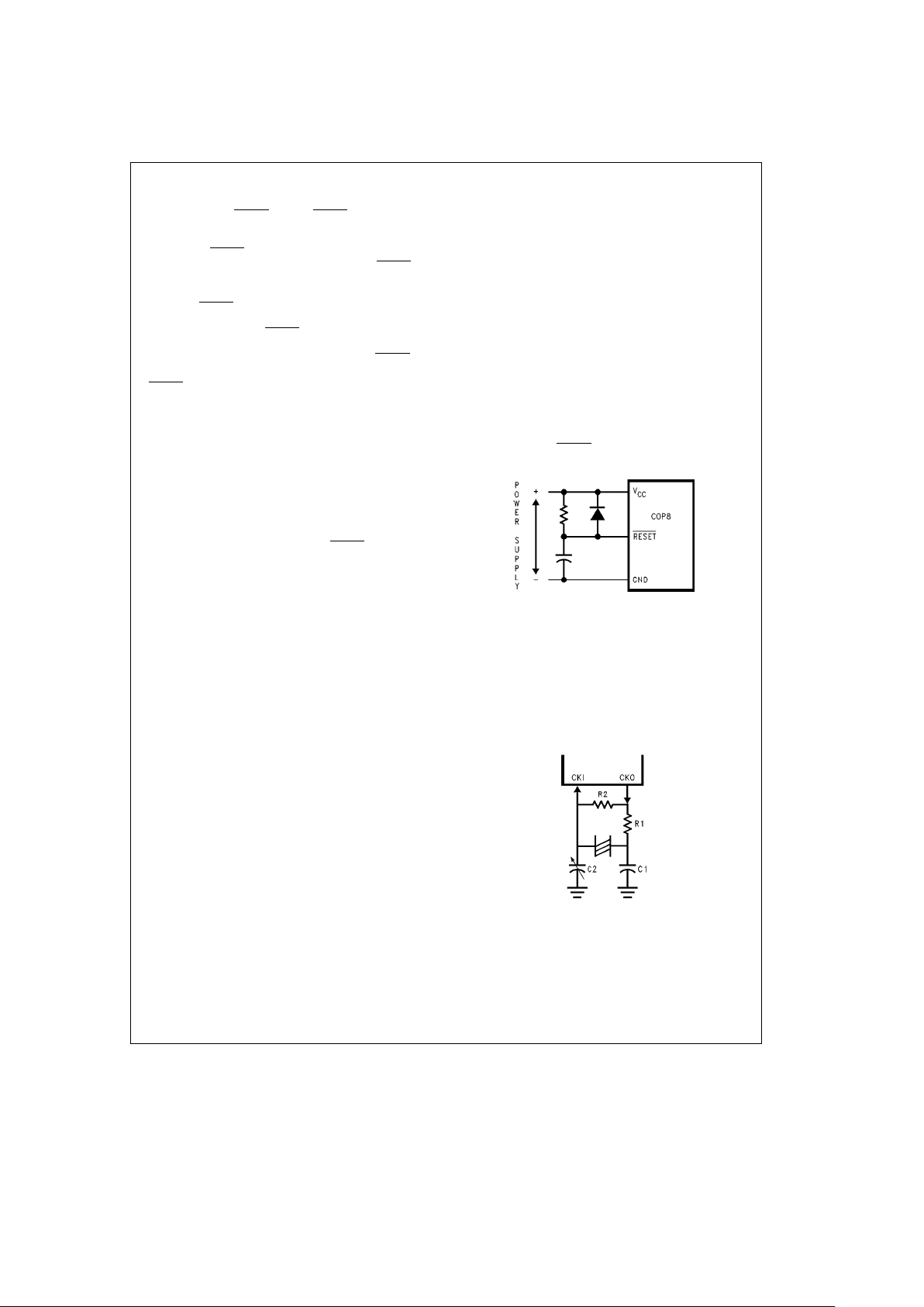
The external RC network shown in
Figure 5
should be used
to ensure that the RESET
pin is held low until the power
supply to the chip stabilizes.
TL/DD/12065– 6
RCl5cPOWER SUPPLY RISE TIME
FIGURE 5. Recommended Reset Circuit
Oscillator Circuits
The chip can be driven by a clock input on the CKI input pin
which can be between DC and 10 MHz. The CKO output
clock is on pin G7 (crystal configuration), The CKI input frequency is divided down by 10 to produce the instruction
cycle clock (t
c
).
Figure 6
shows the Crystal diagram
TL/DD/12065– 7
FIGURE 6. Crystal Diagram
CRYSTAL OSCILLATOR
CKI and CKO can be connected to make a closed loop
crystal (or resonator) controlled oscillator.
http://www.national.com9
Page 10
Oscillator Circuits (Continued)
Table I shows the component values required for various
standard crystal values.
TABLE I. CrystaI Oscillator Configuration, T
A
e
25§C
R1 R2 C1 C2 CKI Freq
Conditions
(kX)(MX) (pF) (pF) (MHz)
0 1 30 30– 36 10 V
CC
e
5V
0 1 30 30– 36 4 V
CC
e
5V
0 1 200 100 – 150 0.455 V
CC
e
5V
Control Registers
CNTRL Register (Address X’00EE)
The Timer1 (T1) and MICROWIRE/PLUS control register
contains the following bits:
SL1 & SL0 Select the MICROWIRE/PLUS clock divide by
(00
e
2, 01e4, 1xe8)
IEDG External interrupt edge polarity select (0eRis-
ing edge, 1
e
Falling edge)
MSEL Selects G5 and G4 as MICROWIRE/PLUS sig-
nals SK and SO respectively
T1C0 Timer T1 Start/Stop control in timer modes
1 and 2
T1 Underflow Interrupt Pending Flag in timer
mode 3
T1C1 Timer T1 mode control bit
T1C2 Timer T1 mode control bit
T1C3 Timer T1 mode control bit
T1C3 T1C2 T1C1 T1C0 MSEL IEDG SL1 SL0
Bit 7 Bit 0
PSW Register (Address X’00EF)
The PSW register contains the following select bits:
GIE GIobaI interrupt enable (enables interrupts)
EXEN EnabIe externaI interrupt
BUSY MICROWIRE/PLUS busy shifting flag
EXPND ExternaI interrupt pending
T1ENA Timer T1 Interrupt Enable for Timer Underflow or
T1A Input capture edge
T1PNDA Timer T1 Interrupt Pending Flag (Autoreload RA
in mode 1, T1 Underflow in Mode 2, T1A capture
edge in mode 3)
C Carry FIag
HC Half Carry Flag
HC C T1PNDA T1ENA EXPND BUSY EXEN GIE
Bit 7 Bit 0
The Half-Carry fIag is aIso affected by aII the instructions
that affect the Carry fIag. The SC (Set Carry) and RC (Reset
Carry) instructions wilI respectiveIy set or clear both the carry flags. In addition to the SC and RC instructions, ADC,
SUBC, RRC and RLC instructions affect the Carry and Half
Carry fIags.
ICNTRL Register (Address X’00E8)
The ICNTRL register contains the foIlowing bits:
T1ENB Timer T1 Interrupt Enable for T1B Input capture
edge
T1PNDB Timer T1 Interrupt Pending Flag for T1B capture
edge
mWEN EnabIe MICROWIRE/PLUS interrupt
mWPND MICROWIRE/PLUS interrupt pending
T0EN Timer T0 Interrupt Enable (Bit 12 toggle)
T0PND Timer T0 Interrupt pending
LPEN L Port Interrupt Enable (Multi-Input Wake up/In-
terrupt)
Bit 7 couId be used as a flag
Unused LPEN T0PND T0EN WPND WEN T1PNDB T1ENB
Bit 7 Bit 0
T2CNTRL Register (Address X’00C6)
The T2CNTRL register contains the following bits:
T2ENB Timer T2 Interrupt Enable for T2B Input capture
edge
T2PNDB Timer T2 Interrupt Pending Flag for T2B capture
edge
T2ENA Timer T2 Interrupt Enable for Timer Underflow or
T2A Input capture edge
T2PNDA Timer T2 Interrupt Pending Flag (Auto reload RA
in mode 1, T2 Underflow in mode 2, T2A capture
edge in mode 3)
T2C0 Timer T2 Start/Stop control in timer modes 1 and
2 Timer T2 Underflow Interrupt Pending Flag in
timer mode 3
T2C1 Timer T2 mode control bit
T2C2 Timer T2 mode control bit
T2C3 Timer T2 mode control bit
T2C3 T2C2 T2C1 T2C0 T2PNDA T2ENA T2PNDB T2ENB
Bit 7 Bit 0
http://www.national.com 10
Page 11
Timers
The device contains a very versatile set of timers (T0, T1,
T2). All timers and associated autoreload/capture registers
power up containing random data.
TIMER T0 (IDLE TIMER)
The device supports applications that require maintaining
reaI time and Iow power with the IDLE mode. This IDLE
mode support is furnished by the IDLE timer T0, which is a
16-bit timer. The Timer T0 runs continuously at the fixed
rate of the instruction cycle cIock, t
c
. The user cannot read
or write to the IDLE Timer T0, which is a count down timer.
The Timer T0 supports the following functions:
#
Exit out of the Idle Mode (See Idle Mode description)
#
Start up delay out of the HALT mode
The IDLE Timer T0 can generate an interrupt when the thirteenth bit toggIes. This toggle is Iatched into the T0PND
pending flag, and wiIl occur every 4 ms at the maximum
clock frequency (t
c
e
1 ms). A control flag T0EN allows the
interrupt from the thirteenth bit of Timer T0 to be enabled or
disabIed. Setting T0EN will enable the interrupt, while resetting it will disable the interrupt.
TIMER T1 AND TIMER T2
The device has a set of two powerful timer/counter blocks,
T1 and T2. The associated features and functioning of a
timer block are described by referring to the timer block Tx.
Since the two timer blocks, T1 and T2 are identical, all comments are equally applicable to either of the two timer
blocks.
Each timer block consists of a 16-bit timer, Tx, and two
supporting 16-bit autoreload/capture registers, RxA and
RxB. Each timer block has two pins associated with it, TxA
and TxB. The pin TxA supports I/O required by the timer
block, while the pin TxB is an input to the timer block. The
powerful and flexible timer block allows the device to easily
perform all timer functions with minimal software overhead.
The timer block has three operating modes: Processor Independent PWM mode, External Event Counter mode, and
Input Capture mode.
The control bits TxC3, TxC2, and TxC1 allow selection of
the different modes of operation.
Mode 1. Processor Independent PWM Mode
As the name suggests, this mode allows the device to generate a PWM signal with very minimal user intervention. The
user only has to define the parameters of the PWM signal
(ON time and OFF time). Once begun, the timer block will
continuously generate the PWM signal completely independent of the microcontroller. The user software services the
timer block only when the PWM parameters require updating.
In this mode the timer Tx counts down at a fixed rate of tc.
Upon every underflow the timer is alternately reloaded with
the contents of supporting registers, RxA and RxB. The very
first underflow of the timer causes the timer to reload from
the register RxA. Subsequent underflows cause the timer to
be reloaded from the registers alternately beginning with the
register RxB.
The Tx Timer control bits, TxC3, TxC2 and TxC1 set up the
timer for PWM mode operation.
Figure 7
shows a block diagram of the timer in PWM mode.
The underfIows can be programmed to toggle the TxA output pin. The underfIows can also be programmed to generate interrupts.
UnderfIows from the timer are alternately latched into two
pending flags, TxPNDA and TxPNDB. The user must reset
these pending fIags under software control. Two control enabIe fIags, TxENA and TxENB, alIow the interrupts from the
timer underflow to be enabled or disabled. Setting the timer
enable flag TxENA wilI cause an interrupt when a timer underflow causes the RxA register to be reloaded into the timer. Setting the timer enable flag TxENB will cause an interrupt when a timer underflow causes the RxB register to be
reloaded into the timer. Resetting the timer enable flags will
disable the associated interrupts.
Either or both of the timer underflow interrupts may be enabled. This gives the user the flexibility of interrupting once
per PWM period on either the rising or falling edge of the
PWM output. Alternatively, the user may choose to interrupt
on both edges of the PWM output.
Mode 2. ExternaI Event Counter Mode
This mode is quite similar to the processor independent
PWM mode described above. The main difference is that
the timer, Tx, is cIocked by the input signal from the TxA pin.
The Tx timer control bits, TxC3, TxC2 and TxC1 allow the
timer to be clocked either on a positive or negative edge
from the TxA pin. Underflows from the timer are Iatched into
the TxPNDA pending flag. Setting the TxENA control flag
will cause an interrupt when the timer underflows.
TL/DD/12065– 8
FIGURE 7. Timer in PWM Mode
http://www.national.com11
Page 12
Timers (Continued)
TL/DD/12065– 9
FIGURE 8. Timer in External Event Counter Mode
In this mode the input pin TxB can be used as an independent positive edge sensitive interrupt input if the TxENB
control flag is set. The occurrence of a positive edge on the
TxB input pin is latched into the TxPNDB flag.
Figure 8
shows a block diagram of the timer in External
Event Counter mode.
Note: The PWM output is not available in this mode since the TxA pin is
being used as the counter input clock.
Mode 3. Input Capture Mode
The device can precisely measure external frequencies or
time external events by placing the timer block, Tx, in the
input capture mode.
In this mode, the timer Tx is constantly running at the fixed
t
c
rate. The two registers, RxA and RxB, act as capture
registers. Each register acts in conjunction with a pin. The
register RxA acts in conjunction with the TxA pin and the
register RxB acts in conjunction with the TxB pin.
The timer value gets copied over into the register when a
trigger event occurs on its corresponding pin. Control bits,
TxC3, TxC2 and TxC1, allow the trigger events to be specified either as a positive or a negative edge. The trigger condition for each input pin can be specified independently.
The trigger conditions can also be programmed to generate
interrupts. The occurrence of the specified trigger condition
on the TxA and TxB pins will be respectively Iatched into the
pending flags, TxPNDA and TxPNDB.
The control flag TxENA allows the interrupt on TxA to be
either enabled or disabled. Setting the TxENA flag enables
interrupts to be generated when the selected trigger condition occurs on the TxA pin. Similarly, the flag TxENB controls the interrupts from the TxB pin.
Underflows from the timer can also be programmed to generate interrupts. Underflows are latched into the timer TxC0
pending flag (the TxC0 control bit serves as the timer underflow interrupt pending flag in the Input Capture mode). Consequently, the TxC0 control bit should be reset when entering the Input Capture mode. The timer underflow interrupt is
enabled with the TxENA control flag. When a TxA interrupt
occurs in the Input Capture mode, the user must check both
the TxPNDA and TxC0 pending flags in order to determine
whether a TxA input capture or a timer underflow (or both)
caused the interrupt.
Figure 9
shows a block diagram of the timer in Input Capture
mode.
TL/DD/12065– 10
FIGURE 9. Timer in Input Capture Mode
http://www.national.com 12
Page 13
Timers (Continued)
TIMER CONTROL FLAGS
The timers T1 and T2 have identical control structures. The
control bits and their functions are summarized below.
TxC0 Timer Start/Stop controI in Modes 1 and 2 (Proc-
essor Independent PWM and External Event
Counter), where 1
e
Start, 0eStop Timer UnderfIow Interrupt Pending Flag in Mode 3 (Input
Capture)
TxPNDA Timer Interrupt Pending Flag
TxPNDB Timer Interrupt Pending Flag
TxENA Timer Interrupt Enable FIag
TxENB Timer Interrupt Enable Flag
1
e
Timer Interrupt EnabIed
0eTimer Interrupt Disabled
TxC3 Timer mode controI
TxC2 Timer mode control
TxC1 Timer mode controI
The timer mode controI bits (TxC3, TxC2 and TxC1) are
detailed beIow:
Capture Timer
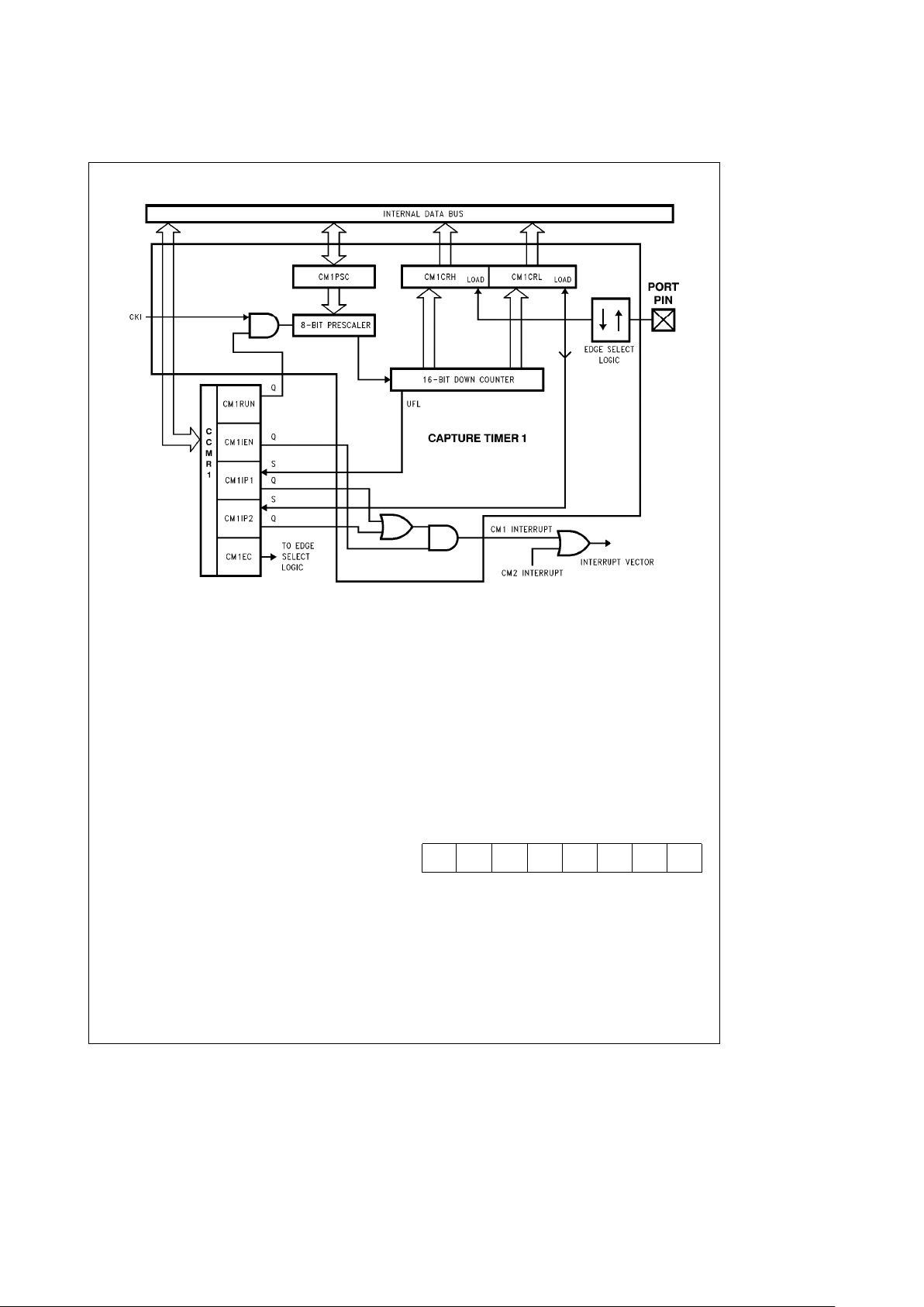
This device contains two independent capture timers, Capture Timer 1 and Capture Timer 2. Each capture timer contains an 8-bit programmable prescaler register, a 16-bit
down counter, a 16-bit input capture register, and capture
edge select Iogic. The 16-bit down counter is clocked at a
specific frequency determined by the value loaded into the
prnscaler register. A selected positive or negative edge
transition on the capture input causes the contents of the
down counter to be latched into the capture register. The
values captured in the registers reflect the eIapsed time between two positive or two negative transitions on the capture input. The time between a positive and negative edge
(a pulse width) may be measured if the selected capture
edge is switched after the first edge is captured. Each capture timer may be stopped/started under software control,
and each capture timer may be configured to interrupt the
microcontroller on an underflow or input capture.
Figure 10
shows the capture timer 1 block diagram.
TABLE II. Timer Mode Control
TxC3 TxC2 TxC1 Timer Mode
Interrupt A Interrupt B Timer
Source Source Counts On
0 0 0 MODE 2 (External Event Counter) Timer Underflow Positive TxB Edge TxA Positive Edge
0 0 1 MODE 2 (External Event Counter) Timer Underflow Positive TxB Edge TxA Negative Edge
1 0 1 MODE 1 (PWM) TxA Toggle Autoreload RA Autoreload RB t
c
1 0 0 MODE 1 (PWM) No TxA Toggle Autoreload RA Autoreload RB t
c
0 1 0 MODE 3 (Capture) Captures: Positive TxA Edge or Positive TxB Edge t
c
TxA Positive Edge Timer Underflow
TxB Positive Edge
1 1 0 MODE 3 (Capture) Captures: Positive TxA Edge or Negative TxB Edge t
c
TxA Positive Edge Timer Underflow
TxB Negative Edge
0 1 1 MODE 3 (Capture) Captures: Negative TxA Edge or Positive TxB Edge t
c
TxA Negative Edge Timer Underflow
TxB Positive Edge
1 1 1 MODE 3 (Capture) Captures: Negative TxA Edge or Negative TxB Edge t
c
TxA Negative Edge Timer Underflow
TxB Negative Edge
http://www.national.com13
Page 14
Timers (Continued)
TL/DD/12065– 11
FIGURE 10. Capture Timer 1 Block Diagram
The registers shown in the block diagram include those for
Capture Timer 1 (CM1), as well as, the capture timer 1 control register. These registers are read/writable (with the exception of the capture registers, which are read-only) and
may be accessed through the data memory address/data
bus. The registers are designated as:
CM1PSC Capture Timer 1 Prescaler (8-bit)
CM1CRL Capture Timer 1 Capture Register (Low-byte),
read-only
CM1CRH Capture Timer 1 Capture Register (High-byte),
read-only
CM2PSC Capture Timer 2 Prescaler (8-bit)
CM2CRL Capture Timer 2 Capture Register (Low-byte),
read-only
CM2CRH Capture Timer 2 Capture Register (High-byte),
read-only
CCMR1 Control Register for Capture Timer 1
CCMR2 Control Register for Capture Timer 2
CONTROL REGISTER BITS
The control bits for Capture Timer 1 (CM1) and Capture
Timer 2 (CM2) are contained in CCMR1 and CCMR2.
The CCMR1 Register Bits are:
CM1RUN CM1 start/stop control bit (1
e
start; 0estop)
CM1IEN CM1 interrupt enable control bit (1eenable
IRQ)
CM1IP1 CM1 interrupt pending bit 1 (1
e
CM1 under-
flowed)
CM1IP2 CM1 interrupt pending bit 2 (1
e
CM1 captured)
CM1EC Select the active edge for capture on CM1 (0
e
rising, 1efalling)
CM1TM CM1 test mode control bit (1especial test path
in test mode. This bit is reserved during normal
operation, and must never be set to one.)
CM1 un- un- CM1 CM1 CM1 CM1 CM1
TM used used EC IP2 IP1 IEN RUN
Bit 7 Bit 0
All interrupt pending bits must be reset by software.
http://www.national.com 14
Page 15

Timers (Continued)
The CCMR2 Register Bits are:
CM2RUN CM2 start/stop control bit (1 start; 0
e
stop)
CM2IEN CM2 interrupt enable control bit (1eenable IRQ)
CM2IP1 CM2 interrupt pending bit 1 (1eCM2 under-
flowed)
CM2IP2 CM2 interrupt pending bit 2 (1
e
CM2 captured)
CM2EC Select the active edge for capture on CM2 (0
e
rising, 1efalling)
CM2TM CM2 test mode control bit (1especiaI test path
in test mode. This bit is reserved during normal
operation, and must never be set to one.)
CM2 un- un- CM2 CM2 CM2 CM2 CM
TM used used EC IP2 IP1 IEN RUN
Bit 7 Bit 0
AII interrupt pending bits must be reset by software.
FUNCTIONAL DESCRIPTION
The capture timer is used to determine the time between
events, where an event is simply a selected edge transition
on the capture input. The resolution of the time measurement is dependent on the frequency at which the down
counter is clocked. The vaIue Ioaded into the prescaler controls this frequency.
The prescaIer is clocked by CKI, while the down counter is
clocked on every underfIow of the prescaler. This means
the prescaIer simpIy divides the CKI cIock before it is fed
into the down counter. The prescaler register must be Ioaded with a vaIue corresponding to the CKI divisor needed to
produce the desired down counter clock. The appropriate
prescaler vaIue can be determined using the following
equation:
Down Counter Clock Frequency
e
CKI/(CMxPSCa1)
The capture input signaI is set up by configuring the port pin
associated with the capture timer as an input. The edge
seIect bit for the capture input is then set or reset according
to the desired transition. If the pin is configured as an input,
the appropriate externaI transition will cause a capture. If
the pin is configured as an output, toggling the data register
bit wiIl cause a capture. If interrupts are used, the capture
timer interrupt pending bits are cIeared and the capture timer interrupt enable bit is set. Both interrupt sources, down
counter underflow and input capture edge, are enabled/disabled with the same CMxIEN bit. The GIE bit must also be
set to enable interrupts. The interrupt signals from the two
capture timers are gated to a single 16-bit interrupt vector
located at addresses 0xE6 and 0xE7.
The capture timer is started by writing a ‘‘1’’ to the capture
timer start/stop bit. Setting this bit also enables the port pin
to be the capture input to the capture timer. The internal
prescaler is loaded with the contents of the prescaler register, and begins counting down. Setting the start/stop bit
also loads the down counter with 0FFFF Hex. The prescaler
is clocked by CKI. An underflow of the prescaler decrements the 16-bit down counter, and reloads the value from
the prescaler register into the prescaler. Each additional underflow of the prescaler decrements the down counter, and
reloads the prescaler from the prescaler register.
If a selected edge transition on the input capture pin occurs,
the contents of the down counter are immediately latched
into the capture register, the down counter is re-initialized to
0FFFF Hex, and the capture input pending flag is set. The
prescaler counter is not loaded. (In order for an input transition to be guaranteed recognized, the signal on the capture input pin must have a low pulse width and a high pulse
width of at least one CKI period.) If interrupts are enabled,
the capture timer generates an interrupt. The prescaler and
down counter continue to operate until a reset condition
occurs or the capture timer start/stop bit is reset. The user
must process capture interrupts faster than the capture input frequency, otherwise input captures may be lost or erroneous values may be read.
If the down counter underflows (changes state from 0000 to
FFFF) before a capture input is detected, the underflow interrupt pending flag is set. If interrupts are enabled, the capture timer generates an interrupt.
The capture timer may be stopped at any time under software control by resetting the capture timer start/stop bit. A
capture may occur before the start/stop bit is physically
cIeared, due to the fully asynchronous nature of the input
capture signal. The user must ensure that the software handles this situation correctly. If the user wishes to process
this capture and interrupts are being used, the capture timer
interrupts should not be disabIed prior to stopping the timer.
If interrupts are not being used, the user should poll the
capture timer pending bits after stopping the timer. If the
user wishes to ignore this capture and interrupts are being
used, the capture timer interrupt service routine should
check that the timer is still running prior to processing capture interrupts. If the user is polling the pending flags, these
flags should be cleared after the timer is stopped. The contents of the prescaler and down counter remain unchanged
while the capture timer is stopped. The capture edge detect
logic is disabled, and no capture takes place even if an
external capture signal occurs. The capture timer may be
restarted under software control by writing a ‘‘1’’ to the
start/stop bit. This causes the prescaler and down counter
to be re-initialized. The prescaler is loaded from the prescaler register, and the down counter is loaded with 0FFFF Hex.
RESET STATE
A reset signal applied to the counter block during normal
operation has the following effects:
#
Clear CCMR1 register
#
Clear CCMR2 register
#
CM1PSC, CMICRL, CM1CRH, CM2PSC, CM2CRL and
CM2CRH are unaffected. (At power-on, the contents of
these registers are undefined.)
The bi-directional port pins are initialized during reset as
HI-Z inputs. Setting the start/stop bits connects the pins to
the capture timers.
http://www.national.com15
Page 16

Timers (Continued)
INITIALIZATION
The user should perform the following initialization prior to
starting the capture timer:
1. Reset the CMxRUN bit
2. Configure the corresponding Port bits as inputs
3. Set the edge control bits CMxEC
4. Reset CMxIP1 (CMxIP1
e
0)
5. Reset CMxIP2 (CMxIP2e0)
6. Load the 8-bit prescaler register CMxPSC with the desired value (from 0 to 255)
7. Set CMxIEN (if interrupts are to be used)
8. Set the Global Interrupt Enable (GIE) bit (if interrupts are
to be used)
9. Set CMxRUN bit to start the capture timer
WARNING
In order to avoid erroneous interrupts, the capture timer interrupts must be disabled prior to setting/resetting the capture edge control bits (CMxEC). In addition, after selecting
the interrupt edge, the pending flags must be reset before
the capture interrupts are enabled or re-enabled. If the initialization sequence outlined above is followed each time
the user aIters the edge control bits, the user is guaranteed
to avoid erroneous interrupts.
Pulse Train Generators
This device contains four independent pulse train generators. Each individual generator is controlled by a corresponding 16-bit counter. Each counter has a 16-bit prescaler and a 16-bit count register. Each counter may be configured to output a selected number of 50% duty cycle pulses.
The contents of the prescaler determine the width of the
output pulses, and the value of the count register determines the number of pulses. Each counter may be stopped/
started under software control, and each counter may be
configured to interrupt the microcontroller on an underflow.
Figure 11
shows the pulse train generator 1 block diagram.
TL/DD/12065– 12
FIGURE 11. Pulse Train Generator 1 Block Diagram
http://www.national.com 16
Page 17

Pulse Train Generators (Continued)
The four 8-bit registers shown in each individual counter in
the block diagram constitute a 16-bit prescaler and a 16-bit
count register. These registers are all read/writable and
may be accessed through the data memory address/data
bus. The registers are designated as:
CxPRL Low-byte of the Prescaler
CxPRH High-byte of the Prescaler
CxCTL Low-byte of the Count Register
CxCTH High-byte of the Count Register
CONTROL REGISTER BITS
The control bits for Counter 1 and Counter 2 are contained
in the CCR1 register. The CCR1 Register bits are:
C1RUN COUNTER1 start/stop control bit (1
e
start; 0
e
stop)
C1IEN COUNTER1 interrupt enable control bit (1een-
able IRQ)
C1IPND COUNTER1 interrupt pending bit (1 counter 1 un-
derflowed)
C1TM COUNTER1 test mode control bit (1
e
special test
path in test mode. This bit is reserved during normal operation, and must never be set to one.)
C2RUN COUNTER2 start/stop control bit (1
e
start; 0
e
stop)
C2IEN COUNTER2 interrupt enable control bit (1een-
able IRQ)
C2IPND COUNTER2 interrupt pending bit (1
e
counter 2
underflowed)
C2TM COUNTER2 test mode control bit (1
e
special test
path. This bit is reserved during normal operation,
and must never be set to one.)
All interrupt pending bits must be reset by software.
C2TM C2 C2 C2 C1TM C1 C1 C1
IPND IEN RUN IPND IEN RUN
Bit 7 Bit 0
The control bits for Counter 3 and Counter 4 are contained
in the CCR2 register. The CCR2 Register bits are:
C3RUN COUNTER3 start stop control bit (1
e
start; 0
e
stop)
C3IEN COUNTER3 interrupt enable control bit (1
e
en-
able IRQ)
C3IPND COUNTER3 interrupt pending Bit (1
e
counter 3
underflowed)
C3TM COUNTER3 test mode control bit (1
e
special test
path. This bit is reserved during normal operation,
and must never be set to one.)
C4RUN COUNTER4 start/stop control bit (1
e
start; 0
e
stop)
C4IEN COUNTER4 interrupt enable control bit (1
e
en-
able IRQ)
C4IPND COUNTER4 interrupt pending bit (1
e
counter 4
underflowed
C4TM COUNTER4 test mode control bit (1
e
special test
path. This bit is reserved during normal operation,
and must never be set to one.)
C4TM C4 C4 C4 C3TM C3 C3 C3
IPND IEN RUN IPND IEN RUN
Bit 7 Bit 0
All interrupt pending bits must be reset by software.
FUNCTIONAL DESCRIPTION
The pulse train generator may be used to produce a series
of output pulses of a given width. The high/low time of a
pulse is determined by the contents of the prescaler. The
number of pulses in a series is determined by the contents
of the count register.
The prescaler is loaded with a value corresponding to the
desired width of the output pulse (t
w
). The high time and low
time of the output signal are each equal to t
w
, therefore the
output signal produced has a 50% duty cycle and a period
equal to 2 * t
w
. The appropriate prescaler value can be
determined using the following equation:
t
w
e
[
(PRH * 256)
a
PRLa1]* t
c
Since PRH and PRL are both 8-bit registers, this equation
allows a maximum t
w
of 65536 tcand a minimum twof one
t
c
. The internal prescaler is automatically loaded from PRH
and PRL when the counter start/stop bit is set.
The count register is loaded with a value corresponding to
the desired number of output pulses. The appropriate count
value is calculated with the following equation:
Number of Pulses
e
CTH * 256aCTLa1
The port pin associated with the counter OUT signal is configured in software as an output, and preset to the desired
start logic level. lf interrupts are to be used, the counter
interrupt pending bit is cleared and the interrupt enable bit is
set. The GIE bit must also be set to enable interrupts. The
interrupt signals from the four counters are gated to a single
interrupt vector located at addresses 0xF0 – 0xF1.
The counter is started by writing a ‘‘1’’ to the counter start/
stop bit. This resets the divide-by-2 counter which produces
the clock signal for the counter register from the prescaler
underflow (See
Figure 11
). It also reloads the internal prescaler and starts the prescaler counting down on the next
rising edge of t
c
. The prescaler is clocked on the rising edge
of t
c
to ensure synchronization. Each subsequent rising
edge of t
c
causes the prescaler to be decremented. When
the prescaler underflows, UFL1 is generated (see
Figure
12
). This signal causes the port pin to toggle. In addition, the
internal prescaler is reloaded with the value from the PRH
and PRL registers. Each additional underflow of the prescaler causes the port pin to toggle and reloads the internal
prescaler.
Every second underflow of the prescaler generates the signal UFL2. (UFL2 occurs at half the frequency of UFL1, or
once per output pulse.) This signal, UFL2, decrements the
count register. Therefore, the count registers are decremented once per output pulse.
http://www.national.com17
Page 18

Pulse Train Generators (Continued)
The underflow of the counter register produces the signal
UFL3. This signal stops the counter by resetting the counter
start/stop bit, and sets the counter interrupt pending flag. If
the counter interrupt is enabled, an interrupt occurs.
The counter may be stopped at any time under software
control by resetting the counter start/stop bit. The contents
of the count register and the output on the associated port
pin are frozen. The counter may be restarted under software
control by setting the start/stop bit. The internal prescaler is
automatically reloaded from PRH and PRL when the counter start/stop bit is set, therefore a full width pulse will be
generated before the output is toggled. The user may also
choose to alter the logic level on the port pin before restarting. This is done by initializing the associated port pin data
register bit. A counter underflow may occur before the start/
stop bit is physically cleared by software. The user must
ensure that the software handles this situation correctly. If
the user wishes to process this underflow and interrupts are
being used, the counter interrupts should not be disabled
prior to stopping the timer. If interrupts are not being used,
the user should poll the counter pending bits after stopping
the timer. If the user wishes to ignore this underflow and
interrupts are being used, the counter interrupt should be
disabled prior to stopping the timer. If the user is polling the
pending flags, these flags should be cleared after the timer
is stopped.
If the default level of the output pin is high (associated port
data register bit is set to ‘‘1’’) and the counter is stopped
during a low level, the low level becomes the default level.
The software must reinitialize the port pin to a high level
before restarting if necessary. The programmer may also
have to adjust the counter value (See
Figure 12
).
RESET STATE
A reset signal applied to the pulse train generator block
during normal operation has the following effects:
#
Counting stops immediately
#
Interrupt enable bit is reset to zero
#
Counter start/stop bit is reset to zero
#
Interrupt pending bit is reset to zero
#
Test mode controI bit is reset to zero
#
PRL, PRH, CTL and CTH are unaffected (At power-on
reset, the contents of the prescaler and count register
are undefined.)
#
Divide-by-2 counter is reset
#
The bi-directional port pins are initialized during reset as
HI-Z inputs. The appropriate bits must be initialized as
outputs, in order to route the Counter OUT signals to the
port pins.
INITIALIZATION
The user should perform the following initialization prior to
starting the counter:
1. Load PRL register
2. Load PRH register
3. Load CTL register
4. Load CTH register
5. Reset CxIPND bit
6. Set CxIEN (if interrupt is to be used)
7. Configure the associated port bit as an output (if OUT is
to be used)
8. Set the Global Interrupt Enable (GIE) bit (if interrupt is to
be used)
9. Set CxRUN bit to start counter
Multiply/Divide
This device contains a multiply/divide block. This block supports a 1 byte x 2 bytes (3 bytes result) multiply or a 3 bytes/
2 bytes (2 bytes result) divide operation. The multiply or
divide operation is executed by setting control bits located
in the multiply/divide control register. The multiply or divide
operands must be placed into the appropriate memory
mapped locations before the operation is initiated.
TL/DD/12065– 13
FIGURE 12. Timing Diagram for PRLe1, PRHe0, CTLe3, CTHe0
http://www.national.com 18
Page 19

Multiply/Divide (Continued)
TABLE III. Multiply/Divide Registers
Register Name
(Address)
Multiplication Assignment Division Assignment
Before Operation After Operation Before Operation After Operation
MDR1 (xx98) Unused Unchanged Low byte of dividend Low byte of result
MDR2 (xx99) Multiplier Low byte of result Middle byte of dividend High byte of result
MDR3 (xx9A) Middle byte of result High byte of dividend Undefined
MDR4 (xx9B) Low byte of multiplicand High byte of result Low byte of divisor Low byte of divisor
MDR5 (xx9C) High byte of multiplicand Unchanged High byte of divisor High byte of divisor
CONTROL REGISTER BITS
The Multiply/Divide control register (MDCR) is located at
address xx9D. It has the following bit assignments:
MULT Start Multiplication Operation (1
e
start)
DIV Start Division Operation (1estart)
DIVOVF Division Overflow (if the result of a division is
greater than 16 bits or the user attempted to divide
by zero; 1
e
error)
Rsvd Rsvd Rsvd Rsvd Rsvd DIV DIV MULT
OVF
Bit 7 Bit 0
After the appropriate MDR registers are loaded, the MULT
and DIV start bits are set by the user to start a multiply or
divide operation. The division operation has priority, if both
bits are set simultaneously. The MULT and DIV bits are
BOTH automatically cleared by hardware at the end of a
divide or multiply operation. Each division operation causes
the DIVOVF flag to be set/reset as appropriate. The
DIVOVF flag is cleared following a multiplication operation.
DIVOVF is a read-only bit. The MULT and DIV bits are read/
writable. Bits 3-7 in MDCR should not be used, as the MULT
and DIV operations will change their values.
MULTIPLY/DIVIDE OPERATION
For the multiply operation, the muItiplicand is placed at addresses xx9B and xx9C. The multiplier is placed at address
xx99. For the divide operation, the dividend is placed at addresses xx98 to xx9A and the divisor is placed at addresses
xx9B to xx9C. In both operations, all operands are interpreted as unsigned values. The divide or multiply operation is
started by setting the appropriate MDCR bit. If both the
MULT and DIV bits are set, the microcontroller performs a
divide operation. (The user is not required to read or clear
the DIVOVF error bit prior to beginning a new multiply/divide operation. This bit is ignored during subsequent operations. However, the next divide operation will overwrite the
error flag as appropriate, and the next multiply operation will
clear it.)
The multiply operation requires 1 instruction cycle to complete. The divide operation requires 2 instruction cycles to
complete. A divide by zero or a division which produces an
overflow requires only 1 instruction cycle to execute. The
MDR1 through MDR5 registers and the MDCR register can
not be read from or written to during a multiply or divide
operation. Any attempt to write into these registers will be
ignored. Any attempt to read these registers will return undefined data.
The result of a multiply is placed in addresses xx99-xx9B.
The result of a divide is placed in addresses xx98-xx99. If a
division by zero is attempted or if the resulting quotient of a
divide operation is more than 16 bits long, then the DIVOVF
bit is set in the multiply/divide control register. The dividend
and the divisor are left unchanged. The divide operation always causes the DIVOVF flag to be set or reset as appropriate. The DIVOVF flag is cleared following a multiply operation.
RESET STATE
A reset signal applied to the device during normal operation
has the following affects:
MDCR is cleared, and any operation in progress is stopped.
MDR1 through MDR5 are undefined.
Power Save Modes
The device offers the user two power save modes of operation: HALT and IDLE. In the HALT mode, all microcontroller
activities are stopped. In the IDLE mode, the on-board oscillator circuitry and timer T0 are active but all other microcontroller activities are stopped. In either mode, all on-board
RAM, registers, I/O states, and timers (with the exception of
T0) are unaltered.
HALT MODE
The device can be placed in the HALT mode by writing a
‘‘1’’ to the HALT flag (G7 data bit). All microcontroller activities, including the clock and timers, are stopped. In the
HALT mode, the power requirements of the device are minimal and the applied voltage (V
CC
) may be decreased to V
r
(V
r
e
2.0V) without altering the state of lhe machine.
The device supports two different ways of exiting the HALT
mode. The first method of exiting the HALT mode is with the
Multi-Input Wakeup feature on the L port. The second method of exiting the HALT mode is by pulling the RESET
pin
low.
Since a crystal or ceramic resonator may be selected as the
oscillator, the Wakeup signal is not allowed to start the chip
running immediately since crystal oscillators and ceramic
resonators have a delayed start up time to reach full amplitude and frequency stability. The IDLE timer is used to generate a fixed deIay to ensure that the oscilIator has indeed
stabilized before allowing instruction execution. In this case,
upon detecting a valid Wakeup signal, only the oscillator
circuitry is enabled. The IDLE timer is loaded with a value of
256 and is clocked with the t
c
instruction cycle clock. The t
c
clock is derived by dividing the oscillator clock down by a
http://www.national.com19
Page 20

Power Save Modes (Continued)
factor of 10. The Schmitt trigger following the CKI inverter
on the chip ensures that the IDLE timer is clocked only
when the oscillator has a sufficiently large amplitude to
meet the Schmitt trigger specifications. This Schmitt trigger
is not part of the oscillator closed loop. The startup timeout
from the IDLE timer enables the clock signals to be routed
to the rest of the chip.
The devices have two mask options associated with the
HALT mode. The first mask option enables the HALT mode
feature, while the second mask option disables the HALT
mode. With the HALT mode enable mask option, the device
will enter and exit the HALT mode as described above. With
the HALT disable mask option, the device cannot be placed
in the HALT mode (writing a ‘‘1’’ to the HALT flag will have
no effect, the HALT flag will remain ‘‘0’’).
IDLE MODE
The device is placed in the IDLE mode by writing a ‘‘1’’ to
the IDLE flag (G6 data bit). In this mode, all activities, except
the associated on-board oscillator circuitry and the IDLE
Timer T0, are stopped.
As with the HALT mode, the device can be returned to normal operation with a reset, or with a Multi-Input Wake up
from the L Port. Alternately, the microcontroller resumes
normal operation from the IDLE mode when the thirteenth
bit (representing 4.096 ms at internal clock frequency of
10 MHz, t
c
e
1 ms) of the IDLE Timer toggles.
This toggle condition of the thirteenth bit of the IDLE Timer
T0 is latched into the T0PND pending flag.
The user has the option of being interrupted with a transition
on the thirteenth bit of the IDLE Timer T0. The interrupt can
be enabled or disabled via the T0EN control bit. Setting the
T0EN flag enables the interrupt and vice versa.
The user can enter the IDLE mode with the Timer T0 interrupt enabled. In this case, when the T0PND bit gets set, the
device will first execute the Timer T0 interrupt service routine and then return to the instruction following the ‘‘Enter
Idle Mode’’ instruction.
Alternatively, the user can enter the IDLE mode with the
IDLE Timer T0 interrupt disabled. In this case, the device
will resume normal operation with the instruction immediately following the ‘‘Enter IDLE Mode’’ instruction.
Note: It is necessary to program two NOP instructions following both the
set HALT mode and set IDLE mode instructions. These NOP instructions are necessary to allow clock resynchronization following the
HALT or IDLE modes.
Multi-Input Wakeup
The Multi-Input Wake Up feature is used to return (wake up)
the device from either the HALT or IDLE modes. Alternately
Multi-Input Wake Up/Interrupt feature may also be used to
generate up to 8 edge selectable external interrupts.
Figure 13
shows the Multi-Input Wake Up logic.
TL/DD/12065– 15
FIGURE 13. Multi-Input Wake Up Logic
http://www.national.com 20
Page 21

Multi-Input Wakeup (Continued)
The Multi-Input Wake Up feature utilizes the L Port. The
user selects which particular L port bit (or combination of L
Port bits) will cause the device to exit the HALT or IDLE
modes. The selection is done through the register WKEN.
The register WKEN is an 8-bit read/write register, which
contains a control bit for every L port bit. Setting a particular
WKEN bit enables a Wake Up from the associated L port
pin.
The user can select whether the trigger condition on the
selected L Port pin is going to be either a positive edge (low
to high transition) or a negative edge (high to low transition).
This selection is made via the register WKEDG, which is an
8-bit control register with a bit assigned to each L Port pin.
Setting the control bit will select the trigger condition to be a
negative edge on that particular L Port pin. Resetting the bit
selects the trigger condition to be a positive edge. Changing
an edge select entails several steps in order to avoid a
Wake Up condition as a result of the edge change. First, the
associated WKEN bit should be reset, followed by the edge
select change in WKEDG. Next, the associated WKPND bit
should be cleared, followed by the associated WKEN bit
being reenabled.
An example may serve to clarify this procedure. Suppose
we wish to change the edge select from positive (low going
high) to negative (high going low) for L Port bit 5, where bit 5
has previously been enabled for an input interrupt. The program would be as follows:
RBIT 5, WKEN
SBIT 5, WKEDG
RBIT 5, WKPND
SB1T 5, WKEN
If the L port bits have been used as outputs and then
changed to inputs with Multi-Input Wake Up/lnterrupt, a
safety procedure should also be followed to avoid wakeup
conditions. After the selected L port bits have been
changed from output to input but before the associated
WKEN bits are enabled, the associated edge select bits in
WKEDG should be set or reset for the desired edge selects,
followed by the associated WKPND bits being cleared,
This same procedure should be used following reset, since
the L port inputs are left floating as a result of reset.
The occurrence of the selected trigger condition for Multi-Input Wake Up is latched into a pending register called
WKPND. The respective bits of the WKPND register will be
set on the occurrence of the selected trigger edge on the
corresponding Port L pin. The user has the responsibility of
clearing these pending flags. Since WKPND is a pending
register for the occurrence of selected wake up conditions,
the device will not enter the HALT mode if any Wake Up bit
is both enabled and pending. Consequently, the user must
clear the pending flags before attempting to enter the HALT
mode.
WKEN, WKPND and WKEDG are all read/write registers,
and are cleared at reset.
PORT L INTERRUPTS
Port L provides the user with an additional eight fully selectable, edge sensitive interrupts which are all vectored into
the same service subroutine.
The interrupt from Port L shares logic with the wake up circuitry. The register WKEN allows interrupts from Port L to
be individually enabled or disabled. The register WKEDG
specifies the trigger condition to be either a positive or a
negative edge. Finally, the register WKPND latches in the
pending trigger conditions.
The GIE (Global Interrupt Enable) bit enables the interrupt
function.
A control flag, LPEN, functions as a global interrupt enable
for Port L interrupts. Setting the LPEN flag will enable interrupts and vice versa. A separate global pending flag is not
needed since the register WKPND is adequate.
Since Port L is also used for waking the device out of the
HALT or lDLE modes, the user can elect to exit the HALT or
IDLE modes either with or without the interrupt enabled. If
he elects to disable the interrupt, then the device will restart
execution from the instruction immediately following the instruction that placed the microcontroller in the HALT or
IDLE modes. In the other case, the device will first execute
the interrupt service routine and then revert to normal operation. (See HALT MODE for clock option wake up information.)
http://www.national.com21
Page 22

UART
The device contains a full-duplex software programmable
UART. The UART (
Figure 14
) consists of a transmit shift
register, a receive shift register and seven addressable registers, as follows: a transmit buffer register (TBUF), a receiver buffer register (RBUF), a UART control and status register (ENU), a UART receive control and status register
(ENUR), a UART interrupt and clock source register (ENUI),
a prescaler select register (PSR) and baud (BAUD) register.
The ENU register contains flags for transmit and receive
functions; this register also determines the length of the
data frame (7, 8 or 9 bits), the value of the ninth bit in transmission, and parity selection bits. The ENUR register flags
framing, data overrun and parity errors while the UART is
receiving.
Other functions of the ENUR register include saving the
ninth bit received in the data frame, enabling or disabling the
UART’s attention mode of operation and providing additional receiver/transmitter status information via RCVG and
XMTG bits. The determination of an internal or external
clock source is done by the ENUI register, as well as selecting the number of stop bits and enabling or disabling transmit and receive interrupts. A control flag in this register can
also select the UART mode of operation: asynchronous or
synchronous.
TL/DD/12065– 16
FIGURE 14. UART Block Diagram
http://www.national.com 22
Page 23

UART (Continued)
UART CONTROL AND STATUS REGISTERS
The operation of the UART is programmed through three
registers: ENU, ENUR and ENUI. The function of the individual bits in these registers is as follows:
ENU-UART Control and Status Register (Address at 0BA)
PEN PSEL1 XBIT9/ CHL1 CHL0 ERR RBFL TBMT
PSEL0
0RW 0RW 0RW 0RW 0RW 0R 0R IR
Bit 7 Bit 0
ENUR-UART Receive Control and Status Register (Address
at 0BB)
DOE FE PE SPARE RBlT9 ATTN XMTG RCVG
0RD 0RD 0RD 0RW* 0R 0RW 0R 0R
Bit 7 Bit 0
ENUI-UART Interrupt and Clock Source Register (Address
at 0BC)
STP2 STP78 ETDX SSEL XRCLK XTCLK ERI ETI
0RW 0RW 0RW 0RW 0RW 0RW 0RW 0RW
Bit 7 Bit 0
* Bit is not used.
0 Bit is cleared on reset.
1 Bit is set to one on reset.
R Bit is read-only; it cannot be written by software.
RW Bit is read/write.
D Bit is cleared on read; when read by software as a
one, it is cleared automatically. Writing to the bit does
not affect its state.
DESCRIPTION OF UART REGISTER BITS
ENUÐUART CONTROL AND STATUS REGISTER
TBMT: This bit is set when the UART transfers a byte of
data from the TBUF register into the TSFT register for transmission. It is automatically reset when software writes into
the TBUF register.
RBFL: This bit is set when the UART has received a complete character and has copied it into the RBUF register. It
is automatically reset when software reads the character
from RBUF.
ERR: This bit is a global UART error flag which gets set if
any or a combination of the errors (DOE, FE, PE) occur.
CHL1, CHL0: These bits select the character frame format.
Parity is not included and is generated/verified by hardware.
CHL1
e
0, CHL0e0 The frame contains eight data bits.
CHL1
e
0, CHL0e1 The frame continues seven data
bits.
CHL1
e
1, CHL0e0 The frame continues nine data bits.
CHL1
e
1, CHL0e1 Loopback Mode selected. Transmit-
ter output internally looped back to
receiver input. Nine bit framing format is used.
XBIT9/PSEL0: Programs the ninth bit for transmission
when the UART is operating with nine data bits per frame.
For seven or eight data bits per frame, this bit in conjunction
with PSEL1 selects parity.
PSEL1, PSEL0: Parity select bits.
PSEL1
e
0, PSEL0e0 Odd Parity (if Parity enabled)
PSEL1e0, PSEL1e1 Odd Parity (if Parity enabled)
PSEL1
e
1, PSEL0e0 Mark(1) (if Parity enabled)
PSEL1e1, PSEL1e1 Space(0) (if Parity enabled)
PEN: This bit enables/disables Parity (7- and 8-bit modes
only).
PEN
e
0 Parity disabled.
PENe1 Parity enabled.
ENURÐUART RECEIVE CONTROL AND STATUS
REGISTER
RCVG: This bit is set high whenever a framing error occurs
and goes low when RDX goes high.
XMTG: This bit is set to indicate that the UART is transmitting. It gets reset at the end of the last frame (end of last
Stop bit).
ATTN: ATTENTION Mode is enabled while this bit is set.
This bit is cleared automatically on receiving a character
with data bit nine set.
RBIT9: Contains the ninth data bit received when the UART
is operating with nine data bits per frame.
SPARE: Reserved for future use.
PE: Flags a Parity Error.
PE
e
0 Indicates no Parity Error has been detected since
the last time the ENUR register was read.
PE
e
1 Indicates the occurrence of a Parity Error.
FE: Flags a Framing Error.
FEe0 Indicates no Framing Error has been detected
since the last time the ENUR register was read.
FE
e
1 Indicates the occurrence of a Framing Error.
DOE: Flags a Data Overrun Error.
DOE
e
0 Indicates no Data Overrun Error has been detect-
ed since the last time the ENUR register was
read.
DOE
e
1 Indicates the occurrence of a Data Overrun Error.
ENUIÐUART INTERRUPT AND CLOCK SOURCE
REGISTER
ETI: This bit enables/disables interrupt from the transmitter
section.
ETI
e
0 Interrupt from the transmitter is disabled.
ETIe1 Interrupt from the transmitter is enabled.
ERI: This bit enables/disables interrupt from the receiver
section.
http://www.national.com23
Page 24

UART (Continued)
ERI
e
0 Interrupt from the receiver is disabled.
ERIe1 Interrupt from the receiver is enabled.
XTCLK: This bit selects the clock source for the transmitter
section.
XTCLK
e
0 The clock source is selected through the PSR
and BAUD registers.
XTCLK
e
1 Signal on CKX (L1) pin is used as the clock.
XRCLK: This bit selects the clock source for the receiver
section.
XRCLK
e
0 The clock source is selected through the PSR
and BAUD registers.
XRCLK
e
1 Signal on CKX (L1) pin is used as the clock.
SSEL: UART mode select.
SSEL
e
0 Asynchronous Mode.
SSELe1 Synchronous Mode.
ETDX: TDX (UART Transmit Pin) is the alternate function
assigned to Port L pin L2; it is selected by setting ETDX bit.
To simulate line break generation, software should reset
ETDX bit and output logic zero to TDX pin through Port L
data and configuration registers.
STP78: This bit is set to program the last Stop bit to be
7/8th of a bit in length.
STP2: This bit programs the number of Stop bits to be transmitted.
STP2
e
0 One Stop bit transmitted.
STP2e1 Two Stop bits transmitted.
Associated I/O Pins
Data is transmitted on the TDX pin and received on the RDX
pin. TDX is the alternate function assigned to Port L pin L2;
it is selected by setting ETDX (in the ENUI register) to one.
RDX is an inherent function of Port L pin L3, requiring no
setup.
The baud rate clock for the UART can be generated onchip, or can be taken from an external source. Port L pin L1
(CKX) is the external clock I/O pin. The CKX pin can be
either an input or an output, as determined by Port L Configuration and Data registers (Bit 1). As an input, it accepts a
clock signal which may be selected to drive the transmitter
and/or receiver. As an output, it presents the internal Baud
Rate Generator output.
UART Operation
The UART has two modes of operation: asynchronous
mode and synchronous mode.
ASYNCHRONOUS MODE
This mode is selected by resetting the SSEL (in the ENUI
register) bit to zero. The input frequency to the UART is 16
times the baud rate.
The TSFT and TBUF registers double-buffer data for transmission. While TSFT is shifting out the current character on
the TDX pin, the TBUF register may be loaded by software
with the next byte to be transmitted. When TSFT finishes
transmitting the current character the contents of TBUF are
transferred to the TSFT register and the Transmit Buffer
Empty Flag (TBMT in the ENU register) is set. The TBMT
flag is automatically reset by the UART when software loads
a new character into the TBUF register. There is also the
XMTG bit which is set to indicate that the UART is transmitting. This bit gets reset at the end of the last frame (end of
last Stop bit). TBUF is a read/write register.
The RSFT and RBUF registers double-buffer data being received. The UART receiver continually monitors the signal
on the RDX pin for a low level to detect the beginning of a
Start bit. Upon sensing this low level, it waits for half a bit
time and samples again. If the RDX pin is still low, the receiver considers this to be a valid Start bit, and the remaining bits in the character frame are each sampled a single
time, at the mid-bit position. Serial data input on the RDX pin
is shifted into the RSFT register. Upon receiving the complete character, the contents of the RSFT register are copied into the RBUF register and the Received Buffer Full Flag
(RBFL) is set. RBFL is automatically reset when software
reads the character from the RBUF register. RBUF is a read
only register. There is also the RCVG bit which is set high
when a framing error occurs and goes low once RDX goes
high. TBMT, XMTG, RBFL and RCVG are read only bits.
SYNCHRONOUS MODE
In this mode data is transferred synchronously with the
clock. Data is transmitted on the rising edge and received
on the falling edge of the synchronous clock.
This mode is selected by setting SSEL bit in the ENUI register. The input frequency to the UART is the same as the
baud rate.
When an external clock input is selected at the CKX pin,
data transmit and receive are performed synchronously with
this clock through TDX/RDX pins.
If data transmit and receive are selected with the CKX pin
as clock output, the device generates the synchronous
clock output at the CKX pin. The internal baud rate generator is used to produce the synchronous clock. Data transmit
and receive are performed synchronously with this clock.
FRAMING FORMATS
The UART supports several serial framing formats
(Figure
15)
. The format is selected using control bits in the ENU,
ENUR and ENUI registers.
The first format (1,1a, 1b, 1c) for data transmission (CHL0
e
1, CHL1e0) consists of Start bit, seven Data bits (excluding parity) and 7/8, one or two Stop bits. In applications
using parity, the parity bit is generated and verified by hardware.
The second format (CHL0
e
0, CHL1e0) consists of one
Start bit, eight Data bits (excluding parity) and 7/8, one or
two Stop bits. Parity bit is generated and verified by hardware.
The third format for transmission (CHL0
e
0, CHL1e1)
consists of one Start bit, nine Data bits and 7/8, one or two
Stop bits. This format also supports the UART ‘‘ATTENTION’’ feature. When operating in this format, all eight bits
of TBUF and RBUF are used for data. The ninth data bit is
transmitted and received using two bits in the ENU and
ENUR registers, called XBIT9 and RBIT9. RBIT9 is a read
only bit. Parity is not generated or verified in this mode.
http://www.national.com 24
Page 25

UART Operation (Continued)
TL/DD/12065– 17
FIGURE 15. Framing Formats
For any of the above framing formats, the last Stop bit can
be programmed to be 7/8th of a bit in length. If two Stop
bits are selected and the 7/8th bit is set (selected), the
second Stop bit will be 7/8th of a bit in length.
The parity is enabled/disabled by PEN bit located in the
ENU register. Parity is selected for 7- and 8-bit modes only.
If parity is enabled (PEN
e
1), the parity selection is then
performed by PSEL0 and PSEL1 bits located in the ENU
register.
Note that the XBIT9/PSEL0 bit located in the ENU register
serves two mutually exclusive functions. This bit programs
the ninth bit for transmission when the UART is operating
with nine data bits per frame. There is no parity selection in
this framing format. For other framing formats XBIT9 is not
needed and the bit is PSEL0 used in conjunction with
PSEL1 to select parity.
The frame formats for the receiver differ from the transmitter in the number of Stop bits required. The receiver only
requires one Stop bit in a frame, regardless of the setting of
the Stop bit selection bits in the control register. Note that
an implicit assumption is made for full duplex UART operation that the framing formats are the same for the transmitter and receiver.
UART INTERRUPTS
The UART is capable of generating interrupts. Interrupts are
generated on Receive Buffer Full and Transmit Buffer Empty. Both interrupts have individual interrupt vectors. Two
bytes of program memory space are reserved for each interrupt vector. The two vectors are located at addresses 0xEC
to 0xEF Hex in the program memory space. The interrupts
can be individually enabled or disabled using Enable Transmit Interrupt (ETl) and Enable Receive Interrupt (ERl) bits in
the ENUI register.
The interrupt from the Transmitter is set pending, and remains pending, as long as both the TBMT and ETl bits are
set. To remove this interrupt, software must either clear the
ETI bit or write to the TBUF register (thus clearing the TBMT
bit).
The interrupt from the receiver is set pending, and remains
pending, as long as both the RBFL and ERI bits are set. To
remove this interrupt, software must either clear the ERl bit
or read from the RBUF register (thus clearing the RBFL bit).
Baud Clock Generation
The clock inputs to the transmitter and receiver sections of
the UART can be individually selected to come either from
an external source at the CKX pin (port L, pin L1) or from a
source selected in the PSR and BAUD registers. Internally,
the basic baud clock is created from the oscillator frequency
through a two-stage divider chain consisting of a 1 – 16 (increments of 0.5) prescaler and an 11-bit binary counter
(Fig-
ure 16)
. The divide factors are specified through two read/
write registers shown in
Figure 17
. Note that the 11-bit Baud
Rate Divisor spills over into the Prescaler Select Register
(PSR). PSR is cleared upon reset.
http://www.national.com25
Page 26

Baud Clock Generation (Continued)
TL/DD/12065– 18
FIGURE 16. UART BAUD Clock Generation
TL/DD/12065– 19
FIGURE 17. UART BAUD Clock Divisor Registers
http://www.national.com 26
Page 27

Baud Clock Generation (Continued)
As shown in Table V, a Prescaler Factor of 0 corresponds to
NO CLOCK. This condition is the UART power down mode
where the UART clock is turned off for power saving purpose. The user must also turn the UART clock off when a
different baud rate is chosen.
The correspondences between the 5-bit Prescaler Select
and Prescaler factors are shown in Table V. There are many
ways to calculate the two divisor factors, but one particularly
effective method would be to achieve a 1.8432 MHz frequency coming out of the first stage. The 1.8432 MHz prescaler output is then used to drive the software programmable baud rate counter to create a 16x clock for the following
baud rates: 110, 134.5, 150, 300, 600, 1200, 1800, 2400,
3600, 4800, 7200, 9600, 19200 and 38400 (Table IV). Other
baud rates may be created by using appropriate divisors.
The 16x clock is then divided by 16 to provide the rate for
the serial shift registers of the transmitter and receivers.
TABLE IV. Baud Rate Divisors
(1.8432 MHz PrescaIer Output)
Baud Baud Rate
Rate Divisor
b
1 (N-1)
110 (110.03) 1046
134.5 (134.58) 855
150 767
300 383
600 191
1200 95
1800 63
2400 47
3600 31
4800 23
7200 15
9600 11
19200 5
38400 2
Note: The entries in Table IV assume a prescaIer output of 1.8432 MHz. In
asynchronous mode the baud rate could be as high as 625k.
TABLE V. Prescaler Factors
Prescaler Prescaler
Select Factor
00000 NO CLOCK
00001 1
00010 1.5
00011 2
00100 2.5
00101 3
00110 3.5
00111 4
01000 4.5
01001 5
01010 5.5
01011 6
01100 6.5
01101 7
01110 7.5
01111 8
10000 8.5
10001 9
10010 9.5
10011 10
10100 10.5
10101 11
10110 11.5
10111 12
11000 12.5
11001 13
11010 13.5
11011 14
11100 14.5
11101 15
11110 15.5
11111 16
http://www.national.com27
Page 28

Baud Clock Generation (Continued)
As an example, considering Asynchronous Mode and a CKI
clock of 4.608 MHz, the prescaler factor selected is:
4.608/1.8432
e
2.5
The 2.5 entry is available in Table V. The 1.8432 MHz prescaler output is then used with proper Baud Rate Divisor
(Table V) to obtain different baud rates. For a baud rate of
19200 e.g., the entry in Table IV is 5.
N
b1e
5(Nb1 is the value from Table IV)
Ne6 (N is the Baud Rate Divisor)
Baud Rate
e
1.8432 MHz/(16c6)e19200
The divide by 16 is performed because in the asynchronous
mode, the input frequency to the UART is 16 times the baud
rate. The equation to calculate baud rates is given below.
The actual Baud Rate may be found from:
BR
e
Fc/(16cNcP)
Where:
BR is the Baud Rate
Fc is the CKI frequency
N is the Baud Rate Divisor (Table IV).
P is the Prescaler Divide Factor selected by the value in the
Prescaler Select Register (Table V)
Note: In the Synchronous Mode, the divisor 16 is replaced by two.
Example:
Asynchronous Mode:
Crystal Frequencye5 MHz
Desired baud ratee9600
Using the above equation N
c
P can be calculated first.
NcPe(5c106)/(16c9600)e32.552
Now 32.552 is divided by each Prescaler Factor (Table V) to
obtain a value closest to an integer. This factor happens to
be 6.5 (P
e
6.5).
N
e
32.552/6.5e5.008 (Ne5)
The programmed value (from Table IV) should be 4 (Nb1).
Using the above values calculated for N and P:
BRe(5c106)/(16c5c6.5)e9615.384
% error
e
(9615.385b9600)/9600e0.16
Effect of HALT/IDLE
The UART logic is reinitialized when either the HALT or
IDLE modes are entered. This reinitialization sets the TBMT
flag and resets all read only bits in the UART control and
status registers. Read/Write bits remain unchanged. The
Transmit Buffer (TBUF) is not affected, but the Transmit
Shift register (TSFT) bits are set to one. The receiver registers RBUF and RSFT are not affected.
The device will exit from the HALT/IDLE modes when the
Start bit of a character is detected at the RDX (L3) pin. This
feature is obtained by using the Multi-Input Wakeup scheme
provided on the device.
Before entering the HALT or IDLE modes the user program
must select the Wakeup source to be on the RDX pin. This
selection is done by setting bit 3 of WKEN (Wakeup Enable)
register. The Wakeup trigger condition is then selected to
be high to low transition. This is done via the WKEDG register (Bit 3 is ‘‘one’’).
If the device is halted and crystal oscillator is used, the
Wake Up signal will not start the chip running immediately
because of the finite start up time requirement of the crystal
oscillator. The idle timer (T0) generates a fixed (256 t
c
) delay to ensure that the oscillator has indeed stabilized before
allowing the device to execute code. The user has to consider this delay when data transfer is expected immediately
after exiting the HALT mode.
Diagnostic
Bits CHARL0 and CHARL1 in the ENU register provide a
Ioopback feature for diagnostic testing of the UART. When
these bits are set to one, the following occur: The receiver
input pin (RDX) is internally connected to the transmitter
output pin (TDX); the output of the Transmitter Shift Register is ‘‘looped back’’ into the Receive Shift Register input. In
this mode, data that is transmitted is immediately received.
This feature allows the processor to verify the transmit and
receive data paths of the UART.
Note that the framing format for this mode is the nine bit
format; one Start bit, nine data bits, and 7/8, one or two
Stop bits. Parity is not generated or verified in this mode.
Attention Mode
The UART Receiver section supports an alternate mode of
operation, referred to as ATTENTION Mode. This mode of
operation is selected by the ATTN bit in the ENUR register.
The data format for transmission must also be selected as
having nine Data bits and either 7/8, one or two Stop bits.
The ATTENTION mode of operation is intended for use in
networking the device with other processors. Typically in
such environments the messages consists of device addresses, indicating which of several destinations should receive them, and the actual data. This Mode supports a
scheme in which addresses are flagged by having the ninth
bit of the data field set to a 1. If the ninth bit is reset to a
zero the byte is a Data byte.
While in ATTENTION mode, the UART monitors the communication flow, but ignores all characters until an address
character is received. Upon receiving an address character,
the UART signals that the character is ready by setting the
RBFL flag, which in turn interrupts the processor if UART
Receiver interrupts are enabled. The ATTN bit is also
cleared automatically at this point, so that data characters
as well as address characters are recognized. Software examines the contents of the RBUF and responds by deciding
either to accept the subsequent data stream (by leaving the
ATTN bit reset) or to wait until the next address character is
seen (by setting the ATTN bit again).
Operation of the UART Transmitter is not affected by selection of this Mode. The value of the ninth bit to be transmitted
is programmed by setting XBIT9 appropriately. The value of
the ninth bit received is obtained by reading RBIT9. Since
this bit is located in ENUR register where the error flags
reside, a bit operation on it will reset the error flags.
http://www.national.com 28
Page 29

Interrupts
The devices supports a vectored interrupt scheme. It supports a total of fourteen interrupt sources. Table VI lists all
the possible device interrupt sources, their arbitration rankings and the memory locations reserved for the interrupt
vector for each source.
Two bytes of program memory space are reserved for each
interrupt source. All interrupt sources except the software
interrupt are maskable. Each of the maskable interrupts
have an Enable bit and one or more Pending bits. A maskable interrupt is active it its associated enable and pending
bits are set. If GlE
e
1 and an interrupt is active, then the
processor will be interrupted as soon as it is ready to start
executing an instruction except if the above conditions happen during the Software Trap service routine. This exception is described in the Software Trap sub-section.
The interruption process is accomplished with the INTR instruction (opcode 00), which is jammed inside the Instruction Register and replaces the opcode about to be executed. The following steps are performed for every interrupt:
1. The GIE (Global Interrupt Enable) bit is reset.
2. The address of the instruction about to be executed is
pushed into the stack.
3. The PC (Program Counter) branches to address 00FF.
This procedure takes 7 t
c
cycles to execute.
At this time, since GIEe0, other maskable interrupts are
disabled. The user is now free to do whatever context
switching is required by saving the context of the machine in
the stack with PUSH instructions. The user would then program a VIS (Vector Interrupt Select) instruction in order to
branch to the interrupt service routine of the highest priority
interrupt enabled and pending at the time of the VIS. Note
that this is not necessarily the interrupt that caused the
branch to address location 00FF Hex prior to the context
switching.
Thus, if an interrupt with a higher rank than the one which
caused the interruption becomes active before the decision
of which interrupt to service is made by the VIS, then the
interrupt with the higher rank will override any lower ones
and will be acknowledged. The lower priority interrupt(s) are
still pending, however, and will cause another interrupt immediately following the completion of the interrupt service
routine associated with the higher priority interrupt just serviced. This lower priority interrupt will occur immediately following the RETI (Return from Interrupt) instruction at the
end of the interrupt service routine just completed.
Inside the interrupt service routine, the associated pending
bit has to be cleared by software. The RETI (Return from
Interrupt) instruction at the end of the interrupt service routine will set the GIE (Global Interrupt Enable) bit, allowing
the processor to be interrupted again if another interrupt is
active and pending.
The VIS instruction looks at all the active interrupts at the
time it is executed and performs an indirect jump to the
beginning of the service routine of the one with the highest
rank.
The addresses of the different interrupt service routines,
called vectors, are chosen by the user and stored in ROM in
a table starting at 01E0 (assuming that VIS is located between 00FF and 01DF). The vectors are 15-bit wide and
therefore occupy 2 ROM locations.
TABLE VI. Interrupt Vector Table
ARBITRATION SOURCE
VECTOR*
RANKING DESCRIPTION
ADDRESS
(Hi-Low Byte)
(1) Highest Software 0yFE – 0yFF
(2) Reserved 0yFC–0yFD
(3) External G0 0yFA-0yFB
(4) Timer T0 Underflow 0yF8–0yF9
(5) Timer T1 T1A/Underflow 0yF6–0yF7
(6) Timer T1 T1B 0yF4-0yF5
(7) Microwire/PIus Busy Low 0yF2– 0yF3
(8) Counters 0yF0 – 0yF1
(9) UART Receive 0yEE – 0yEF
(10) UART Transmit 0yEC –0yED
(11) Timer T2 T2A/Underflow 0yEA–0yEB
(12) Timer T2 T2B 0yE8–0yE9
(13) Capture Timer 1 and 2 0yE6–0yE7
(14) Unused 0yE4–0yE5
(15) Port L/Wakeup 0yE2–0yE3
(16) Lowest Default VIS Reserved 0yE0– 0yE1
* y is a variable which represents the VIS block. VIS and the vector table must be located in the same 256-byte block except if VIS is located at the last address of a
block, In this case, the table must be in the next block.
http://www.national.com29
Page 30

Interrupts (Continued)
VIS and the vector table must be located in the same
256-byte block (0y00 to 0yFF) except if VIS is located at the
last address of a block. In this case, the table must be in the
next block. The vector table cannot be inserted in the first
256-byte block (y
i
0).
The vector of the maskable interrupt with the lowest rank is
located at 0yE0 (Hi-Order byte) and 0yE1 (Lo-Order byte)
and so forth in increasing rank number. The vector of the
maskable interrupt with the highest rank is located at 0yFA
(Hi-Order byte) and 0yFB (Lo-Order byte).
The Software Trap has the highest rank and its vector is
located at 0yFE and 0yFF.
If, by accident, a VIS gets executed and no interrupt is active, then the PC (Program Counter) will branch to a vector
located at 0yE0 –0yE1.
Warning:
A Default VIS interrupt handler routine must be present. As
a minimum, this handler should confirm that the GIE bit is
cleared (this indicates that the interrupt sequence has been
taken), take care of any required housekeeping, restore
context and return. Some sort of Warm Restart procedure
should be implemented. These events can occur without
any error on the part of the system designer or programmer.
Note: There is always the possibility of an interrupt occurring during an
instruction which is attempting to reset the GIE bit or any other interrupt enable bit. If this occurs when a single cycle instruction is being
used to reset the interrupt enable bit, the interrupt enable bit will be
reset but an interrupt may still occur. This is because interrupt processing is started at the same time as the interrupt bit is being reset.
To avoid this scenario, the user should always use a two-, three- or
four-cycle instruction to reset interrupt enable bits.
Figure 18
shows the Interrupt block diagram.
SOFTWARE TRAP
The Software Trap (ST) is a special kind of non-maskable
interrupt which occurs when the INTR instruction (used to
acknowledge interrupts) is fetched from ROM and placed
inside the instruction register. This may happen when the
PC is pointing beyond the available ROM address space or
when the stack is over-popped.
When an ST occurs, the user can re-initialize the stack
pointer and do a recovery procedure (similar to reset, but
not necessarily containing all of the same initialization procedures) before restarting.
The occurrence of an ST is latched into the ST pending bit.
The GIE bit is not affected and the ST pending bit (not
accessible by the user) is used to inhibit other interrupts
and to direct the program to the ST service routine with the
VIS instruction. The RPND instruction is used to clear the
software interrupt pending bit. This pending bit is also
cleared on reset.
The ST has the highest rank among all interrupts.
Nothing (except another ST) can interrupt an ST being
serviced.
TL/DD/12065– 20
FIGURE 18. Interrupt Block Diagram
http://www.national.com 30
Page 31

Detection of Illegal Conditions
The device can detect various illegal conditions resulting
from coding errors, transient noise, power supply voltage
drops, runaway programs, etc.
Reading of undefined ROM gets zeroes. The opcode for
software interrupt is 00. If the program fetches instructions
from undefined ROM, this will force a software interrupt,
thus signaling that an illegal condition has occurred.
The subroutine stack grows down for each call (jump to
subroutine), interrupt, or PUSH, and grows up for each return or POP. The stack pointer is initialized to RAM location
06F Hex during reset. Consequently, if there are more returns than calls, the stack pointer will point to addresses
070 and 071 Hex (which are undefined RAM). Undefined
RAM from addresses 070 to 07F (Segment 0), 140 to 17F
(Segment 1), and all other segments (i.e., Segments 3...
etc.) is read as all 1’s, which in turn will cause the program
to return to address 7FFF Hex. This is an undefined ROM
location and the instruction fetched (all 0’s) from this location will generate a software interrupt signaling an illegal
condition.
Thus, the chip can detect the following illegal conditions:
1. Executing from undefined ROM
2. Over ‘‘POP’’ing the stack by having more returns than
calls.
When the software interrupt occurs, the user can re-initialize
the stack pointer and do a recovery procedure before restarting (this recovery program is probably similar to that
following reset, but might not contain the same program
initialization procedures). The recovery program should reset the software interrupt pending bit using the RPND instruction.
MICROWIRE/PLUS
MICROWIRE/PLUS is a serial synchronous communications interface. The MICROWIRE/PLUS capability enables
the device to interface with any of National Semiconductor’s
MICROWIRE peripherals (i.e., A/D converters, display drivers, E2PROMs etc.) and with other microcontrollers which
support the MICROWIRE interface. It consists of an 8-bit
serial shift register (SIO) with serial data input (SI), serial
data output (SO) and serial shift clock (SK).
Figure 19
shows a block diagram of the MICROWIRE/PLUS logic.
The shift clock can be selected from either an internal
source or an external source. Operating the MlCROWIRE/
PLUS arrangement with the internal clock source is called
the Master mode of operation. Similarly, operating the
MICROWIRE/PLUS arrangement with an external shift
clock is called the Slave mode of operation.
The CNTRL register is used to configure and control the
MICROWIRE/PLUS mode. To use the MICROWIRE/PLUS,
the MSEL bit in the CNTRL register is set to one. In the
master mode, the SK clock rate is selected by the two bits,
SL0 and SL1, in the CNTRL register. Table VII details the
different clock rates that may be selected.
TABLE VII. MICROWIRE/PLUS
Master Mode Clock Select
SL1 SL0 SK Period
00 2
c
t
c
01 4
c
t
c
1x 8
c
t
c
Where tcis the instruction cycle clock
TL/DD/12065– 21
FIGURE 19. MICROWIRE/PLUS Block Diagram
http://www.national.com31
Page 32

MICROWIRE/PLUS (Continued)
MICROWIRE/PLUS OPERATION
Setting the BUSY bit in the PSW register causes the
MICROWIRE/PLUS to start shifting the data. It gets reset
when eight data bits have been shifted. The user may reset
the BUSY bit by software to allow less than 8 bits to shift. If
enabled, an interrupt is generated when eight data bits have
been shifted. The device may enter the MICROWIRE/PLUS
mode either as a Master or as a Slave.
Figure 20
shows
how two devices, microcontrollers and several peripherals
may be interconnected using the MICROWIRE/PLUS arrangements.
Warning:
The SIO register should only be loaded when the SK clock
is low. Loading the SIO register while the SK clock is high
will resuIt in undefined data in the SIO register. SK clock is
normally low when not shifting.
Setting the BUSY flag when the input SK clock is high in the
MICROWIRE/PLUS slave mode may cause the current SK
clock for the SIO shift register to be narrow. For safety, the
BUSY flag should only be set when the input SK clock is
low.
MICROWIRE/PLUS Master Mode Operation
In the MICROWIRE/PLUS Master mode of operation the
shift clock (SK) is generated internally by the device. The
MICROWIRE Master always initiates all data exchanges.
The MSEL bit in the CNTRL register must be set to enable
the SO and SK functions onto the G Port. The SO and SK
pins must also be selected as outputs by setting appropriate
bits in the Port G configuration register. Table VIII summarizes the bit settings required for Master mode of operation.
MICROWIRE/PLUS Slave Mode Operation
In the MICROWIRE/PLUS Slave mode of operation the SK
clock is generated by an external source. Setting the MSEL
bit in the CNTRL register enables the SO and SK functions
onto the G Port. The SK pin must be selected as an input
and the SO pin is selected as an output pin by setting and
resetting the appropriate bits in the Port G configuration register. Table VIII summarizes the settings required to enter
the Slave mode of operation.
TABLE VIII. MICROWIRE Mode Settings
G4 (SO) G5 (SK) G4 G5
Operation
Config. Bit Config. Bit Fun. Fun.
1 1 SO Int. MICROWIRE/PLUS
SK Master
0 1 TRI- Int. MICROWlRE/PLUS
STATE SK Master
1 0 SO Ext. MlCROWlRE/PLUS
SK Slave
0 0 TRl- Ext. MICROWlRE/PLUS
STATE SK Slave
This table assumes that the control flag MSEL is set.
The user must set the BUSY flag immediately upon entering
the Slave mode. This will ensure that all data bits sent by
the Master will be shifted properly. After eight clock pulses
the BUSY flag will be cleared and the sequence may be
repeated.
Alternate SK Phase Operation
The device allows either the normal SK clock or an alternate
phase SK clock to shift data in and out of the SIO register. in
both the modes the SK is normally low. In the normal mode
data is shifted in on the rising edge of the SK clock and the
data is shifted out on the falling edge of the SK clock. The
SIO register is shifted on each falling edge of the SK clock.
In the alternate SK phase operation, data is shifted in on the
falling edge of the SK clock and shifted out on the rising
edge of the SK clock.
A control flag, SKSEL, allows either the normal SK clock or
the alternate SK clock to be selected. Resetting SKSEL
causes the MICROWIRE/PLUS logic to be clocked from the
normal SK signal. Setting the SKSEL flag selects the alternate SK clock. The SKSEL is mapped into the G6 configuration bit. The SKSEL flag will power up in the reset condition,
selecting the normal SK signal.
TL/DD/12065– 22
FIGURE 20. MICROWIRE/PLUS Application
http://www.national.com 32
Page 33

Memory Map
All RAM, ports and registers (except A and PC) are mapped into data memory address space.
ADDRESS
CONTENTS
S/ADD REG
0000 to 006F 112 On-Chip RAM Bytes
0070 to 007F Unused RAM Address Space
(reads as all 1’s)
xx80 to xx8F Unused RAM Address Space
(reads undefined data)
xx90 Port E Data Register
xx91 Port E Configuration Register
xx92 Port E Input Pins (read only)
xx93 Reserved
xx94 Port F Data Register
xx95 Port F Configuration Register
xx96 Port F Input Pins (read only)
xx97 Reserved
xx98 Dividend or Result Byte (MDR1)
xx99 Dividend/Multiplier or Result Byte (MDR2)
xx9A Dividend/Result Byte or Undefined (MDR3)
xx9B Divisor/Multiplicand or Result Byte (MDR4)
xx9C Divisor or Multiplicand Byte(MDR5)
xx9D MuItiply/Divide Control Register (MDCR)
xx9E Counter Control 1 Register (CCR1)
xx9F Counter Control 2 Register (CCR2)
xxA0 Counter 1 Prescaler Lower Byte (C1PRL)
xxA1 Counter 1 Prescaler Upper Byte (C1PRH)
xxA2 Counter 1 Count Register Lower Byte (C1CTL)
xxA3 Counter 1 Count Register Upper Byte (C1CTH)
xxA4 Counter 2 Prescaler Lower Byte (C2PRL)
xxA5 Counter 2 Prescaler Upper Byte (C2PRH)
xxA6 Counter 2 Count Register Lower Byte (C2CTL)
xxA7 Counter 2 Count Register Upper Byte (C2CTH)
xxA8 Counter 3 Prescaler Lower Byte (C3PRL)
xxA9 Counter 3 Prescaler Upper Byte (C3PRH)
xxAA Counter 3 Count Register Lower Byte (C3CTL)
xxAB Counter 3 Count Register Upper Byte (C3CTH)
xxAC Counter 4 Prescaler Lower Byte (C4PRL)
xxAD Counter 4 Prescaler Upper Byte (C4PRH)
xxAE Counter 4 Count Register Lower Byte (C4CTL)
xxAF Counter 4 Count Register Upper Byte (C4CTH)
xxB0 Capture Timer 1 Prescaler Register (CM1 PSC)
xxB1 Capture Timer 1 Lower Byte (CM1CRL) Read-Only
xxB2 Capture Timer 1 Upper Byte (CM1CRH) Read-Only
xxB3 Capture Timer 2 Prescaler Register (CM2PSC)
xxB4 Capture Timer 2 Lower Byte (CM2CRL) Read-Only
xxB5 Capture Timer 2 Upper Byte (CM2CRH) Read-Only
xxB6 Capture Timer 1 Control Register (CCMR1)
xxB7 Capture Timer 2 Control Register (CCMR2)
xxB8 UART Transmit Buffer (TBUF)
xxB9 UART Receive Buffer (RBUF)
xxBA UART Control and Status Register (ENU)
http://www.national.com33
Page 34

Memory Map (Continued)
ADDRESS
CONTENTS
S/ADD REG
xxBB UART Receive Control and Status Register (ENUR)
xxBC UART Interrupt and Clock Source Register (ENUI)
xxBD UART Baud Register (BAUD)
xxBE UART Prescaler Select Register (PSR)
xxBF Reserved for UART
xxC0 Timer T2 Lower Byte
xxC1 Timer T2 Upper Byte
xxC2 Timer T2 Autoload Register T2RA Lower Byte
xxC3 Timer T2 Autoload Register T2RA Upper Byte
xxC4 Timer T2 Autoload Register T2RB Lower Byte
xxC5 Timer T2 Autoload Register T2RB Upper Byte
xxC6 Timer T2 Control Register
xxC7 Reserved
xxC8 MIWU Edge Select Register (WKEDG)
xxC9 MlWU Enable Register (WKEN)
xxCA MlWU Pending Register (WKPND)
xxCB Reserved
xxCC Reserved
xxCD to xxCF Reserved
xxD0 Port L Data Register
xxD1 Port L Configuration Register
xxD2 Port L Input Pins (Read Only)
xxD3 Reserved for Port L
xxD4 Port G Data Register
xxD5 Port G Configuration Register
xxD6 Port G Input Pins (Read Only)
xxD7 Port l Input Pins (Read Only)
xxD8 Port C Data Register
xxD9 Port C Configuration Register
xxDA Port C Input Pins (Read Only)
xxDB Reserved for Port C
xxDC Port D
xxDD to xxDF Reserved for Port D
xxE0 to xxE5 Reserved for EE Control Registers
xxE6 Timer T1 Autoload Register T1RB Lower Byte
xxE7 Timer T1 Autoload Register T1RB Upper Byte
xxE8 ICNTRL Register
xxE9 MICROWIRE Shift Register
xxEA Timer T1 Lower Byte
xxEB Timer T1 Upper Byte
xxEC Timer T1 Autoload Register T1RA Lower Byte
xxED Timer T1 Autoload Register T1RA Upper Byte
xxEE CNTRL Control Register
xxEF PSW Register
xxF0 to xxFB On-chip RAM Mapped as Registers
xxFC X Register
xxFD SP Register
xxFE B Register
xxFF S Register
0100 to 017F
0200 to 027F On Chip RAM Bytes (384 Bytes)
0300 to 037F
Reading memory locations 0070H-007FH (Segment 0) will return all ones. Reading unused memory locations between 0080H-00F0 Hex (Segment 0) will return
undefined data. Reading memory locations from other segments (i.e., segment 4, segment 5, etc.) will return all ones.
http://www.national.com 34
Page 35

Memory Map (Continued)
ADDRESSING MODES
There are ten addressing modes, six for operand addressing and four for transfer of control.
OPERAND ADDRESSING MODES
Register Indirect
This is the ‘‘normal’’ addressing mode. The operand is the
data memory addressed by the B pointer or X pointer.
Register Indirect (with auto post Increment or
decrement of pointer)
This addressing mode is used with the LD and X instructions. The operand is the data memory addressed by the B
pointer or X pointer. This is a register indirect mode that
automatically post increments or decrements the B or X register after executing the instruction.
Direct
The instruction contains an 8-bit address field that directly
points to the data memory for the operand.
ImmedIate
The instruction contains an 8-bit immediate field as the operand.
Short Immediate
This addressing mode is used with the Load B Immediate
instruction. The instruction contains a 4-bit immediate field
as the operand.
Indirect
This addressing mode is used with the LAID instruction. The
contents of the accumuiator are used as a partial address
(lower 8 bits of PC) for accessing a data operand from the
program memory.
TRANSFER OF CONTROL ADDRESSING MODES
Relative
This mode is used for the JP instruction, with the instruction
field being added to the program counter to get the new
program location. JP has a range from
b
31 toa32 to allow
a 1-byte relative jump (JP
a
1 is implemented by a NOP
instruction). There are no ‘‘pages’’ when using JP, since all
15 bits of PC are used.
Absolute
This mode is used with the JMP and JSR instructions, with
the instruction field of 12 bits replacing the lower 12 bits of
the program counter (PC). This allows jumping to any location in the current 4k program memory segment.
Absolute Long
This mode is used with the JMPL and JSRL instructions,
with the instruction field of 15 bits replacing the entire 15
bits of the program counter (PC). This allows jumping to any
location up to 32k in the program memory space.
Indirect
This mode is used with the JID instruction. The contents of
the accumulator are used as a partial address (lower 8 bits
of PC) for accessing a location in the program memory. The
contents of this program memory location serve as a partial
address (lower 8 bits of PC) for the jump to the next instruction.
Note: The VIS is a special case of the Indirect Transfer of Control address-
ing mode, where the double byte vector associated with the interrupt
is transferred from adjacent addresses in the program memory into
the program counter (PC) in order to jump to the associated interrupt
service routine.
Instruction Set
Register and Symbol Definition
Registers
A 8-Bit Accumulator Register
B 8-Bit Address Register
X 8-Bit Address Register
SP 8-Bit Stack Pointer Register
PC 15-Bit Program Counter Register
PU Upper 7 Bits of PC
PL Lower 8 Bits of PC
C 1 Bit of PSW Register for Carry
HC 1 Bit of PSW Register for Half Carry
GIE 1 Bit of PSW Register for Global
Interrupt Enable
VU Interrupt Vector Upper Byte
VL Interrupt Vector Lower Byte
Symbols
[B]
Memory Indirectly Addressed by B
Register
[X]
Memory Indirectly Addressed by X
Register
MD Direct Addressed Memory
Mem Direct Addressed Memory or[B
]
Meml Direct Addressed Memory or[B]or
Immediate Data
Imm 8-Bit Immediate Data
Reg Register Memory: Addresses F0 to FF
(Includes B, X and SP)
Bit Bit Number (0 to 7)
w
Loaded with
Ý
Exchanged with
http://www.national.com35
Page 36

INSTRUCTION SET
ADD A,MemI ADD AwAaMemI
ADC A,Meml ADD with Carry A
w
AaMemIaC, CwCarry, HCwHalf Carry
SUBC A,Meml Subtract with Carry A
w
AbMemIaC, CwCarry, HCwHalf Carry
AND A,Meml Logical AND A
w
A and MemI
ANDSZ A,lmm Logical AND lmmed., Skip if Zero Skip next if (A and Imm)e0
OR A,Meml Logical OR A
w
A or MemI
XOR A,Meml Logical EXclusive OR A
w
A xor MemI
IFEQ MD,lmm IF EQual Compare MD and lmm, Do next if MDelmm
IFEQ A,Meml IF EQual Compare A and Meml, Do next if A
e
Meml
IFNE A,Meml IF Not Equal Compare A and Meml, Do next if A
i
Meml
IFGT A,Meml IF Greater Than Compare A and Meml, Do next if A
l
Meml
lFBNE
Ý
IF B Not Equal Do next if lower 4 bits of BiImm
DRSZ Reg Decrement Reg., Skip if Zero Reg
w
Regb1, Skip if Rege0
SBIT
Ý
,Mem Set BIT 1 to bit, Mem (bite0 to 7 immediate)
RBIT
Ý
,Mem Reset BIT 0 to bit, Mem
lFBIT
Ý
,Mem IF BIT If bitÝ, A or Mem is true do next instruction
RPND Reset PeNDing Flag Reset Software Interrupt Pending Flag
X A,Mem EXchange A with Memory AÝMem
XA,
[
X
]
EXchange A with Memory[X
]
A
Ý
[X]
LD A,Meml LoaD A with Memory A
w
MemI
LD A,[X
]
LoaD A with Memory[X
]
A
w
[X]
LD B, Imm LoaD B with Immed. B
w
Imm
LD Mem, Imm LoaD Memory Immed. Mem
w
Imm
LD Reg, Imm LoaD Register Memory Immed. RegwImm
XA,
[
B
g
]
EXchange A with Memory[B
]
A
Ý
[B]
,(B
w
Bg1)
XA,
[
X
g
]
EXchange A with Memory[X
]
A
Ý
[X]
,(X
w
Xg1)
LD A,[B
g
]
LoaD A with Memory[B
]
A
w
[B]
,(B
w
Bg1)
LD A,[X
g
]
LoaD A with Memory[X
]
A
w
[X]
,(X
w
Xg1)
LD
[
B
g
]
,lmm LoaD Memory[B]lmmed.
[B]
w
Imm, (BwBg1)
CLR A CLeaR A Aw0
INC A INCrement A AwAa1
DEC A DECrement A A
w
Ab1
LAID Load A InDirect from ROM A
w
ROM (PU, A)
DCOR A Decimal CORrect A A
w
BCD correction of A (follows ADC, SUBC)
RRC A Rotate A Right thru C C
xA7x
...xA0xC
RLC A Rotate A Left thru C C
wA7w
...wA0wC
SWAP A SWAP nibbles of A A7...A4
Ý
A3...A0
SC Set C C
w
1, HCw1
RC Reset C Cw0, HCw0
IFC IF C If C is true, do next instruction
IFNC IF Not C If C is not true, do next instruction
POP A POP the stack into A SP
w
SPa1, A
w
[SP]
PUSH A PUSH A onto the stack
[SP]
w
A, SPwSPb1
VIS Vector to Interrupt Service Routine PU
w
[VU]
,PL
w
[VL]
JMPL Addr. Jump absolute Long PC
w
ii (iie15 bits, 0 to 32k)
JMP Addr. Jump absolute PC9...0
w
i(ie12 bits)
JP Disp. Jump relative short PCwPCar(risb31 toa32, except 1)
JSRL Addr. Jump SubRoutine Long
[SP]
w
PL,[SPb1
]
w
PU, SPb2, PCwii
JSR Addr Jump SubRoutine
[SP]
w
PL,[SPb1
]
w
PU, SPb2,PC9...0wi
JID Jump InDirect PL
w
ROM (PU, A)
RET RETurn from subroutine SP
a
2, PL
w
[SP]
,PU
w
[
SP
b
1
]
RETSK RETurn and SKip SP
a
2, PL
w
[SP]
,PU
w
[
SP
b
1], skip next instruction
RETI RETurn from Interrupt SP
a
2, PL
w
[SP]
,PU
w
[
SP
b
1], GIEw1
INTR Generate an Interrupt
[SP]
w
PL,[SPb1
]
w
PU, SPb2, PCw0FF
NOP No OPeration PCwPCa1
http://www.national.com 36
Page 37

Instruction Execution Time
Most instructions are single byte (with immediate addressing mode instructions taking two bytes).
Most single byte instructions take one cycle time to execute.
Skipped instructions require x number of cycles to be skipped, where x equals the number of bytes in the skipped instruction
opcode.
See the BYTES and CYCLES per INSTRUCTION table for details.
Bytes and Cycles per InstructIon
The following table shows the number of bytes and cycles for each instruction in the format of byte/cycle.
Arithmetic and Logic Instructions
[B]
Direct Immed.
ADD 1/1 3/4 2/2
ADC 1/1 3/4 2/2
SUBC 1/1 3/4 2/2
AND 1/1 3/4 2/2
OR 1/1 3/4 2/2
XOR 1/1 3/4 2/2
IFEQ 1/1 3/4 2/2
IFGT 1/1 3/4 2/2
IFBNE 1/1
DRSZ 1/3
SBIT 1/1 3/4
RBIT 1/1 3/4
lFBIT 1/1 3/4
RPND 1/1
Instructions UsingA&C
CLRA 1/1
INCA 1/1
DECA 1/1
LAID 1/3
DCORA 1/1
RRCA 1/1
RLCA 1/1
SWAPA 1/1
SC 1/1
RC 1/1
IFC 1/1
IFNC 1/1
PUSHA 1/3
POPA 1/3
ANDSZ 2/2
Transfer of Control Instructions
JMPL 3/4
JMP 2/3
JP 1/3
JSRL 3/5
JSR 2/5
JID 1/3
VIS 1/5
RET 1/5
RETSK 1/5
RETI 1/5
INTR 1/7
NOP 1/1
Memory Transfer Instructions
Register
Direct Immed.
Register Indirect
Indirect Auto Incr. and Decr.
[B][
X
][
B
a
,B
b
][
X
a,Xb
]
XA,* 1/1 1/3 2/3 1/2 1/3
LD A, * 1/1 1/3 2/3 2/2 1/2 1/3
LD B, Imm 1/1 (IF B
k
16)
LD B, Imm 2/2 (IF Bl15)
LD Mem, Imm 2/2 3/3 2/2
LD Reg, Imm 2/3
IFEQ MD, Imm 3/3
Note: *
e
l
Memory location addressed by B or X or directly.
Mask Options
The mask programmable options are shown below. The options are programmed at the same time as the ROM pattern
submission.
OPTION 1: CLOCK CONFIGURATION
e
1 Crystal Oscillator (CKI/10)
G7 (CKO) is clock generator output to crystal/resonator with CKI being the clock input
OPTION 2: HALT
e
1 Enable HALT mode
e
2 Disable HALT mode
OPTION 3: BONDING OPTIONS
e
1 68 Pins PLCC
The chip can be driven by a clock input on the CKI input pin
which can be between DC and 10 MHz. The CKO output
clock is on pin G7 (if clock option
e
1 has been selected).
The CKI input frequency is divided down by 10 to produce
the instruction cycle clock (1/t
c
).
http://www.national.com37
Page 38

Lower Nibble
Opcode Table
Upper Nibble
FE D C B A 9 8 76 5 4 3 2 1 0
JP
b
15 JP
b
31 LD 0F0,
Ý
i DRSZ 0F0 RRCA RC ADC A, ADC A,
[
B
]
IFBIT ANDSZ LD B,
Ý
0F IFBNE 0 JSR JMP JP
a
17 INTR 0
Ý
i0,
[
B
]
A,
Ý
i x000 – x0FF x000 –x0FF
JP
b
14 JP
b
30 LD 0F1,
Ý
i DRSZ 0F1 * SC SUBC A, SUBC A,
[
B
]
IFBIT * LD B,
Ý
0E IFBNE 1 JSR JMP JP
a
18 JP
a
21
Ý
i1,
[
B
]
x100–x1FF x100– x1FF
JP
b
13 JP
b
29 LD 0F2,
Ý
i DRSZ 0F2 X A, X A, IFEQ A, IFEQ A,
[
B
]
IFBIT * LD B,
Ý
0D IFBNE 2 JSR JMP JP
a
19 JP
a
32
[
X
a
][
B
a
] Ý
i2,
[
B
]
x200–x2FF x200– x2FF
JP
b
12 JP
b
28 LD 0F3,
Ý
i DRSZ 0F3 X A, X A, IFGT A, IFGT A,
[
B
]
IFBIT * LD B,
Ý
0C IFBNE 3 JSR JMP JP
a
20 JP
a
43
[
X
b
][
B
b
] Ý
i3,
[
B
]
x300–x3FF x300– x3FF
JP
b
11 JP
b
27 LD 0F4,
Ý
i DRSZ 0F4 VIS LAID ADD A, ADD A,
[
B
]
IFBIT CLRA LD B,
Ý
0B IFBNE 4 JSR JMP JP
a
21 JP
a
54
Ý
i4,
[
B
]
x400–x4FF x400– x4FF
JP
b
10 JP
b
26 LD 0F5,
Ý
i DRSZ 0F5 RPND JID AND A, AND A,
[
B
]
IFBIT SWAPA LD B,
Ý
0A IFBNE 5 JSR JMP JP
a
22 JP
a
65
Ý
i5,
[
B
]
x500–x5FF x500– x5FF
JP
b
9JP
b
25 LD 0F6,
Ý
i DRSZ 0F6 X A,
[
X
]
XA,
[
B
]
XOR A, XOR A,
[
B
]
IFBIT DCORA LD B,
Ý
09 IFBNE 6 JSR JMP JP
a
23 JP
a
76
Ý
i6,
[
B
]
x600–x6FF x600– x6FF
JP
b
8JP
b
24 LD 0F7,
Ý
i DRSZ 0F7 **OR A,
Ý
iORA,
[
B
]
IFBIT PUSHA LD B,
Ý
08 IFBNE 7 JSR JMP JP
a
24 JP
a
87
7,
[
B
]
x700–x7FF x700– x7FF
JP
b
7JP
b
23 LD 0F8,
Ý
i DRSZ 0F8 NOP RLCA LD A,
Ý
i IFC SBIT RBIT LD B,
Ý
07 IFBNE 8 JSR JMP JP
a
25 JP
a
98
0,
[
B
]
0,
[
B
]
x800–x8FF x800– x8FF
JP
b
6JP
b
22 LD 0F9,
Ý
i DRSZ 0F9 IFNE IFEQ IFNE IFNC SBIT RBIT LD B,
Ý
06 IFBNE 9 JSR JMP JP
a
26 JP
a
10 9
A,
[
B
]
Md,
Ý
iA,
Ý
i1,
[
B
]
1,
[
B
]
x900–x9FF x900– x9FF
JP
b
5JP
b
21 LD 0FA,
Ý
i DRSZ 0FA LD A, LD A, LD
[
B
a
]
, INCA SBIT RBIT LD B,
Ý
05 IFBNE 0A JSR JMP JP
a
27 JP
a
11 A
[
X
a
][
B
a
] Ý
i2,
[
B
]
2,
[
B
]
xA00–xAFF xA00 –xAFF
JP
b
4JP
b
20 LD 0FB,
Ý
i DRSZ 0FB LD A, LD A, LD
[
B
b
]
, DECA SBIT RBIT LD B,
Ý
04 IFBNE 0B JSR JMP JP
a
28 JP
a
12 B
[
X
b
][
B
b
] Ý
i3,
[
B
]
3,
[
B
]
xB00–xBFF xB00 –xBFF
JP
b
3JP
b
19 LD 0FC,
Ý
i DRSZ 0FC LD Md,
Ý
i JMPL X A,Md POPA SBIT RBIT LD B,
Ý
03 IFBNE 0C JSR JMP JP
a
29 JP
a
13 C
4,
[
B
]
4,
[
B
]
xC00–xCFF xC00– xCFF
JP
b
2JP
b
18 LD 0FD,
Ý
i DRSZ 0FD DIR JSRL LD A,Md RETSK SBIT RBIT LD B,
Ý
02 IFBNE 0D JSR JMP JP
a
30 JP
a
14 D
5,
[
B
]
5,
[
B
]
xD00–xDFF xD00 – xDFF
JP
b
1JP
b
17 LD 0FE,
Ý
i DRSZ 0FE LD A,
[
X
]
LD A,
[
B
]
LD
[
B
]
,
Ý
i RET SBIT RBIT LD B,
Ý
01 IFBNE 0E JSR JMP JP
a
31 JP
a
15 E
6,
[
B
]
6,
[
B
]
xE00–xEFF xE00 – xEFF
JP
b
0JP
b
16 LD 0FF,
Ý
i DRSZ 0FF **LD B,
Ý
i RETI SBIT RBIT LD B,
Ý
00 IFBNE 0F JSR JMP JP
a
32 JP
a
16 F
7,
[
B
]
7,
[
B
]
xF00–xFFF xF00 –xFFF
Where,
i is the immediate data
Md is a directly addressed memory location
* is an unused opcode
Note: The opcode 60 Hex is also the opcode for IFBIT
Ý
i,A.
http://www.national.com 38
Page 39

Development Support
SUMMARY
#
iceMASTER: IM-COP8/400ÐFull feature in-circuit emulation for all COP8 products. A full set of COP8 Basic and
Feature Family device and package specific probes are
available.
#
COP8 Debug Module: Moderate cost in-circuit emulation
and development programming unit.
#
COP8 Evaluation and Programming Unit: EPUCOP888GGÐlow cost In-circuit simulation and development programming unit.
#
Assembler: COP8-DEV-IBMA. A DOS installable cross
development Assembler, Linker, Librarian and Utility
Software Development Tool Kit.
#
C Compiler: COP8C. A DOS installable cross development Software Tool Kit.
#
OTP/EPROM Programmer Support: Covering needs
from engineering prototype, pilot production to full production environments.
iceMASTER (IM) IN-CIRCUIT EMULATION
The iceMASTER IM-COP8/400 is a full feature, PC based,
in-circuit emulation tool developed and marketed by MetaLink Corporation to support the whole COP8 family of products. National is a resale vendor for these products.
See
Figure 21
for configuration.
The iceMASTER IM-COP8/400 with its device specific
COP8 Probe provides a rich feature set for developing, testing and maintaining product:
#
Real-time in-circuit emulation; full 2.4V –5.5V operation
range, full DC-10 MHz clock. Chip options are programmable or jumper selectable.
#
Direct connection to application board by package compatible socket or surface mount assembly.
#
Full 32 kbytes of loadable programming space that overlays (replaces) the on-chip ROM or EPROM. On-chip
RAM and I/O blocks are used directly or recreated on
the probe as necessary.
#
Full 4k frame synchronous trace memory. Address, instruction, and 8 unspecified, circuit connectable trace
lines. Display can be HLL source (e.g., C source), assembly or mixed.
#
A full 64k hardware configurable break, trace on, trace
oft control, and pass count increment events.
#
Tool set integrated interactive symbolic debuggerÐsupports both assembler (COFF) and C Compiler (.COD)
linked object formats.
#
Real time peformance profiling analysis; selectable bucket definition.
#
Watch windows, content updated automatically at each
execution break.
#
Instruction by instruction memory/register changes displayed on source window when in single step operation.
#
Single base unit and debugger software reconfigurable to
support the entire COP8 family; only the probe personality needs to change. Debugger software is processor customized, and reconfigured from a master model file.
#
Processor specific symbolic display of registers and bit
level assignments, configured from master model file.
#
Halt/Idle mode notification.
#
On-line HELP customized to specific processor using
master model file.
#
Includes a copy of COP8-DEV-IBMA assembler and linker SDK.
IM Order Information
Base Unit
IM-COP8/400-1 iceMASTER base unit, 110V
power supply
IM-COP8/400-2 iceMASTER base unit, 220V
power supply
iceMASTER Probe
MHW-888GW68PWPC 68 PLCC
TL/DD/12065– 31
FIGURE 21. COP8 iceMASTER Environment
http://www.national.com39
Page 40

Development Support (Continued)
iceMASTER DEBUG MODULE (DM)
The iceMASTER Debug Module is a PC based, combination
in-circuit emulation tool and COP8 based OTP/EPROM programming tool developed and marketed by MetaLink Corporation to support the whole COP8 family of products. National is a resale vendor for these products.
See
Figure 22
for configuration.
The iceMASTER Debug Module is a moderate cost development tool. It has the capability of in-circuit emulation for a
specific COP8 microcontroller and in addition serves as a
programming tool for COP8 OTP and EPROM product families. Summary of features is as follows:
#
Real-time in-circuit emulation; full operating voltage
range operation, full DC-10 MHz clock.
#
All processor I/O pins can be cabled to an application
development board with package compatible cable to
socket and surface mount assembly.
#
Full 32 kbytes of loadable programming space that overlays (replaces) the on-chip ROM or EPROM. On-chip
RAM and I/O blocks are used directly or recreated as
necessary.
#
100 frames of synchronous trace memory. The display
can be HLL source (C source), assembly or mixed. The
most recent history prior to a break is available in the
trace memory.
#
Configured break points; uses INTR instruction which is
modestly intrusive.
#
SoftwareÐonly supported features are selectable.
#
Tool set integrated interactive symbolic debuggerÐsupports both assembler (COFF) and C Compiler (.COD)
SDK linked object formats.
#
Instruction by instruction memory/register changes displayed when in single step operation.
#
Debugger software is processor customized, and reconfigured from a master model file.
#
Processor specific symbolic display of registers and bit
level assignments, configured from master model file.
#
Halt/Idle mode notification.
#
Programming menu supports full product line of programmable OTP and EPROM COP8 products. Program data
is taken directly from the overlay RAM.
#
Programming of 44 PLCC and 68 PLCC parts requires
external programming adapters.
#
Includes wallmount power supply.
#
On-board VPPgenerator from 5V input or connection to
external supply supported. Requires V
PP
level adjustment per the family programming specification (correct
level is provided on an on-screen pop-down display).
#
On-line HELP customized to specific processor using
master model file.
#
Includes a copy of COP8-DEV-IBMA assembler and linker SDK.
DM Order Information
Debug Module Unit
COP8-DM/888GW
Cable Adapters
DM-COP8/68P 68 PLCC
TL/DD/12065– 32
FIGURE 22. COP8-DM Environment
http://www.national.com 40
Page 41

Development Support (Continued)
COP8 ASSEMBLER/LINKER SOFTWARE
DEVELOPMENT TOOL KIT
National Semiconductor offers a relocateable COP8 macro
cross assembler, linker, librarian and utility software development tool kit. Features are summarized as follows:
#
Basic and Feature Family instruction set by ‘‘device’’
type.
#
Nested macro capability.
#
Extensive set of assembler directives.
#
Supported on PC/DOS platform.
#
Generates National standard COFF output files.
#
Integrated Linker and Librarian.
#
Integrated utilities to generate ROM code file outputs.
#
DUMPCOFF utility.
This product is integrated as a part of MetaLink tools as a
development kit, fully supported by the MetaLink debugger.
It may be ordered separately or it is bundled with the MetaLink products at no additional cost.
Order-Information
Assembler SDK
COP8-DEV-IBMA Assembler SDK on installable
3.5
×
PC/DOS Floppy Disk Drive
format. Periodic upgrades and
most recent version is available
on National’s BBS and Internet.
COP8 C COMPILER
A C Compiler is developed and marketed by Byte Craft Limited. The COP8C compiler is a fully integrated development
tool specifically designed to support the compact embedded configuration of the COP8 family of products. Features
are summarized as follows:
#
ANSI C with some restrictions and extensions that optimize development for the COP8 embedded application.
#
BITS data type extension. Register declarationÝpragma
with direct bit level definitions.
#
C language support for interrupt routines.
#
Expert system, rule based code generation and optimization.
#
Performs consistency checks against the architectural
definitions of the target COP8 device.
#
Generates program memory code.
#
Supports linking of compiled object or COP8 assembled
object formats.
#
Global optimization of linked code.
#
Symbolic debug load format fully source level supported
by the MetaLink debugger.
SINGLE CHIP OTP/EMULATOR SUPPORT
The COP8 family is supported by single chip OTP emulators. For detailed information refer to the emulator specific
datasheet and the emulator selection table below:
OTP Emulator Ordering Information
Device Number
Clock
Package Emulates
Option
COP87L88GWV-XE Crystal/ 68 PLCC COP888GW
HALT En
INDUSTRY WIDE OTP/EPROM PROGRAMMING
SUPPORT
Programming support, in addition to the MetaLink development tools, is provided by a full range of independent approved vendors to meet the needs from the engineering
laboratory to full production.
Approved List
Manufacturer
North
Europe Asia
America
BP (800) 225-2102
a
49-8152-4183
a
852-234-16611
Microsystems (713) 688-4600
a
49-8856-932616
a
852-2710-8121
Fax: (713) 688-0920
Data I/O (800) 426-1045
a
44-0734-440011 Call
(206) 881-6444 North America
Fax: (206) 882-1043
HI–LO (510) 623-8860 Call Asia
a
886-2-764-0215
Fax:
a
886-2-756-6403
ICE (800) 624-8949
a
44-1226-767404
Technology (919) 430-7915 Fax: 0-1226-370-434
MetaLink (800) 638-2423
a
49-80 9156 96-0
a
852-737-1800
(602) 926-0797 Fax:a49-80 9123 86
Fax: (602) 693-0681
Systems (408) 263-6667
a
41-1-9450300
a
886-2-917-3005
General Fax:
a
886-2-911-1283
Needhams (916) 924-8037
Fax: (916) 924-8065
http://www.national.com41
Page 42

Development Support (Continued)
AVAILABLE LITERATURE
For more information, please see the COP8 Basic Family
User’s Manual, Literature Number 620895, COP8 Feature
Family User’s Manual, Literature Number 620897 and National’s Family of 8-bit Microcontrollers COP8 Selection
Guide, Literature Number 630009.
DIAL-A-HELPER SERVICE
Dial-A-Helper is a service provided by the Microcontroller
Applications group. The Dial-A-Helper is an Electronic Information System that may be accessed as a Bulletin Board
System (BBS) via data modem, as an FTP site on the Internet via standard FTP client application or as an FTP site on
the Internet using a standard Internet browser such as Netscape or Mosaic.
The Dial-A-Helper system provides access to an automated
information storage and retrieval system. The system capabilities include a MESSAGE SECTION (electronic mail,
when accessed as a BBS) for communications to and from
the Microcontroller Applications Group and a FILE SECTION which consists of several file areas where valuable
application software and utilities could be found.
DIAL-A-HELPER BBS via a Standard Modem
Modem: CANADA/U.S.: (800) NSC-MICRO
(800) 672-6427
EUROPE: (
a
49) 0-8141-351332
Baud: 14.4k
Set-Up: Length: 8-Bit
Parity: None
Stop Bit: 1
Operation: 24 Hours, 7 Days
DIAL-A-HELPER via FTP
ftp nscmicro.nsc.com
user: anonymous
password: username
@
yourhost.site.domain
DIAL-A-HELPER via a WorldWide Web Browser
ftp://nscmicro.nsc.com
National Semiconductor on the WorldWide Web
See us on the WorldWide Web at: http://www.national.com
CUSTOMER RESPONSE CENTER
Complete product information and technical support is available from National’s customer response centers.
CANADA/ Tel: (800) 272-9959
U.S.:
email: support@tevm2.nsc.com
EUROPE: email: europe.support@nsc.com
Deutsch Tel:a49 (0) 180-530 85 85
English Tel:a49 (0) 180-532 78 32
Fran3ais Tel:a49 (0) 180-532 93 58
Italiano Tel:a49 (0) 180-534 16 80
JAPAN: Tel:
a
81-043-299-2309
S.E. ASIA: Beijing Tel: (a86) 10-6856-8601
Shanghai Tel: (a86) 21-6415-4092
Hong Kong Tel: (a852) 2737-1600
Korea Tel: (a82) 2-3771-6909
Malaysia Tel: (a60-4) 644-9061
Singapore Tel: (a65) 255-2226
Taiwan Tel:a886-2-521-3288
AUSTRALIA: Tel: (a61) 3-9558-9999
INDIA: Tel: (a91) 80-559-9467
http://www.national.com 42
Page 43

http://www.national.com43
Page 44

COP888GW 8-Bit Microcontroller with Pulse Train Generators and Capture Modules
Physical Dimensions inches (millimeters) unless otherwise noted
68-Lead Molded Plastic Chip Carrier
Order Number COP888GW-XXX/V
NS Package Number V68A
LIFE SUPPORT POLICY
NATIONAL’S PRODUCTS ARE NOT AUTHORIZED FOR USE AS CRITICAL COMPONENTS IN LIFE SUPPORT
DEVICES OR SYSTEMS WITHOUT THE EXPRESS WRITTEN APPROVAL OF THE PRESIDENT OF NATIONAL
SEMICONDUCTOR CORPORATION. As used herein:
1. Life support devices or systems are devices or 2. A critical component is any component of a life
systems which, (a) are intended for surgical implant support device or system whose failure to perform can
into the body, or (b) support or sustain life, and whose be reasonably expected to cause the failure of the life
failure to perform, when properly used in accordance support device or system, or to affect its safety or
with instructions for use provided in the labeling, can effectiveness.
be reasonably expected to result in a significant injury
to the user.
National Semiconductor National Semiconductor National Semiconductor National Semiconductor
Corporation Europe Hong Kong Ltd. Japan Ltd.
1111 West Bardin Road Fax:
a
49 (0) 180-530 85 86 13th Floor, Straight Block, Tel: 81-043-299-2308
Arlington, TX 76017 Email: europe.support@nsc.com Ocean Centre, 5 Canton Rd. Fax: 81-043-299-2408
Tel: 1(800) 272-9959 Deutsch Tel:
a
49 (0) 180-530 85 85 Tsimshatsui, Kowloon
Fax: 1(800) 737-7018 English Tel:
a
49 (0) 180-532 78 32 Hong Kong
Fran3ais Tel:
a
49 (0) 180-532 93 58 Tel: (852) 2737-1600
http://www.national.com
Italiano Tel:a49 (0) 180-534 16 80 Fax: (852) 2736-9960
National does not assume any responsibility for use of any circuitry described, no circuit patent licenses are implied and National reserves the right at any time without notice to change said circuitry and specifications.
 Loading...