

Datasheet COP8SCR9HVA8, COP8SBR9LVA8, COP8SBR9KMT8, COP8SBR9IMT8, COP8SBR9HVA8 Datasheet (NSC)
...Page 1

COP8SBR9/COP8SCR9/COP8SDR9
8-Bit CMOS Flash Based Microcontroller with 32k
Memory, Virtual EEPROM and Brownout
1.0 General Description
The COP8SBR9/SCR9/SDR9 Flash based microcontrollers
are highly integrated COP8
Flash memory and advanced features including Virtual EEPROM, High Speed Timers, USART, and Brownout Reset.
Devices included in this datasheet:
Device
COP8SBR9 32k 1k 2.7V to 2.9V
COP8SCR9 32k 1k 4.17V to 4.5V
COP8SDR9 32k 1k No Brownout
™
Feature core devices, with 32k
Flash Program
Memory
(bytes)
RAM
(bytes)
Brownout
This single-chip CMOS device is suited for applications requiring a full featured, in-system reprogrammable controller
with large memory and low EMI. The same device is used for
development, pre-production and volume production with a
range of COP8 software and hardware development tools.
Voltage
I/O
Pins
37,39,49,
59
37,39,49,
59
37,39,49,
59
Packages Temperature
44 LLP,
44/68 PLCC,
48/56 TSSOP
44 LLP,
44/68 PLCC,
48/56 TSSOP
44 LLP,
44/68 PLCC,
48/56 TSSOP
−40˚C to +85˚C
−40˚C to +85˚C
−40˚C to +125˚C
−40˚C to +85˚C
−40˚C to +125˚C
August 2003
COP8SBR9/COP8SCR9/COP8SDR9 8-Bit CMOS Flash Based Microcontroller with 32k Memory,
Virtual EEPROM and Brownout
2.0 Features
KEY FEATURES
n 32 kbytes Flash Program Memory with Security Feature
n Virtual EEPROM using Flash Program Memory
n 1 kbyte volatile RAM
n USART with on chip baud generator
n 2.7V–5.5V In-System Programmability of Flash
n High endurance - 100k Read/Write Cycles
n Superior data retention - 100 years
n Dual Clock Operation with HALT/IDLE Power Save
Modes
n Three 16-bit timers:
— Timers T2 and T3 can operate at high speed (50 ns
resolution)
— Processor Independent PWM mode
— External Event counter mode
— Input Capture mode
n Brown-out Reset (COP8SBR9/SCR9)
OTHER FEATURES
n Single supply operation: 2.7V– 5.5V
n Quiet Design (low radiated emissions)
n Multi-Input Wake-up with optional interrupts
n MICROWIRE/PLUS (Serial Peripheral Interface
Compatible)
n Clock Doubler for 20 MHz operation from 10 MHz
Oscillator, with 0.5 µs Instruction Cycle
n Thirteen multi-source vectored interrupts servicing:
— External Interrupt
— USART (2)
— Idle Timer T0
— Three Timers (each with 2 interrupts)
— MICROWIRE/PLUS Serial peripheral interface
— Multi-Input Wake-Up
— Software Trap
n Idle Timer with programmable interrupt interval
n 8-bit Stack Pointer SP (stack in RAM)
n Two 8-bit Register Indirect Data Memory Pointers
n True bit manipulation
n WATCHDOG and Clock Monitor logic
n Software selectable I/O options
— TRI-STATE
— Push-Pull Output
— Weak Pull Up Input
n Schmitt trigger inputs on I/O ports
n High Current I/Os
n Temperature range: –40˚C to +85˚C and –40˚C to
+125˚C (COP8SCR9/SDR9)
n Packaging: 44 and 68 PLCC, 44 LLP, 48 and 56 TSSOP
n True In-System, Real time emulation and debug offered
by MetaLink’s Development Systemstools available
®
Output/High Impedance Input
COP8™is a trademark of National Semiconductor Corporation.
© 2003 National Semiconductor Corporation DS101389 www.national.com
Page 2

3.0 Block Diagram
COP8SBR9/COP8SCR9/COP8SDR9
4.0 Ordering Information
COP8 SB R 9 H VA 8
Family and
Feature Set
Indicator
SB = Low Brownout Voltage
SC = High Brownout Voltage
SD = No Brownout
Part Numbering Scheme
Program
Memory
Size
R = 32k 9 = Flash H = 44 Pin
Program
Memory
Type
No. Of Pins
I=48Pin
k=56Pin
L = 68 Pin
Package
Type
LQ = LLP
MT = TSSOP
VA = PLCC
10138901
Temperature
7 = -40 to +125˚C
8 = -40 to +85˚C
www.national.com 2
Page 3

Table of Contents
1.0 General Description ..................................................................................................................................... 1
2.0 Features ....................................................................................................................................................... 1
3.0 Block Diagram .............................................................................................................................................. 2
4.0 Ordering Information .................................................................................................................................... 2
5.0 Connection Diagrams ................................................................................................................................... 6
6.0 Architectural Overview ............................................................................................................................... 10
6.1 EMI REDUCTION .................................................................................................................................... 10
6.2 IN-SYSTEM PROGRAMMING AND VIRTUAL EEPROM ...................................................................... 10
6.3 DUAL CLOCK AND CLOCK DOUBLER ................................................................................................. 10
6.4 TRUE IN-SYSTEM EMULATION ............................................................................................................ 10
6.5 ARCHITECTURE ................................................................................................................................... 10
6.6 INSTRUCTION SET ............................................................................................................................... 10
6.6.1 Key Instruction Set Features ............................................................................................................. 10
6.6.2 Single Byte/Single Cycle Code Execution ....................................................................................... 10
6.6.3 Many Single-Byte, Multi-Function Instructions .................................................................................. 10
6.6.4 Bit-Level Control ................................................................................................................................ 11
6.6.5 Register Set ....................................................................................................................................... 11
6.7 PACKAGING/PIN EFFICIENCY .............................................................................................................. 11
7.0 Absolute Maximum Ratings ....................................................................................................................... 12
8.0 Electrical Characteristics ............................................................................................................................ 12
9.0 Pin Descriptions ......................................................................................................................................... 17
9.1 EMULATION CONNECTION ................................................................................................................... 18
10.0 Functional Description .............................................................................................................................. 19
10.1 CPU REGISTERS ................................................................................................................................. 19
10.2 PROGRAM MEMORY ........................................................................................................................... 19
10.3 DATA MEMORY .................................................................................................................................... 19
10.4 DATA MEMORY SEGMENT RAM EXTENSION .................................................................................. 19
10.4.1 Virtual EEPROM .............................................................................................................................. 20
10.5 OPTION REGISTER ............................................................................................................................. 20
10.6 SECURITY ............................................................................................................................................ 21
10.7 RESET ................................................................................................................................................... 21
10.7.1 External Reset ................................................................................................................................. 22
10.7.2 On-Chip Brownout Reset ................................................................................................................. 22
10.8 OSCILLATOR CIRCUITS ...................................................................................................................... 24
10.8.1 Oscillator .......................................................................................................................................... 24
10.8.2 Clock Doubler .................................................................................................................................. 24
................................................................................................................................................................... 0
10.9 CONTROL REGISTERS ....................................................................................................................... 25
10.9.1 CNTRL Register (Address X'00EE) ................................................................................................. 25
10.9.2 PSW Register (Address X'00EF) ..................................................................................................... 25
10.9.3 ICNTRL Register (Address X'00E8) ................................................................................................ 25
10.9.4 T2CNTRL Register (Address X'00C6) ............................................................................................. 25
10.9.5 T3CNTRL Register (Address X'00B6) ............................................................................................. 26
10.9.6 HSTCR Register (Address X'00AF) ................................................................................................ 26
10.9.7 ITMR Register (Address X'00CF) .................................................................................................... 26
11.0 In-System Programming ........................................................................................................................... 27
11.1 INTRODUCTION ................................................................................................................................... 27
11.2 FUNCTIONAL DESCRIPTION .............................................................................................................. 27
11.3 REGISTERS .......................................................................................................................................... 27
11.3.1 ISP Address Registers ..................................................................................................................... 27
11.3.2 ISP Read Data Register .................................................................................................................. 28
11.3.3 ISP Write Data Register ................................................................................................................... 28
11.3.4 ISP Write Timing Register ................................................................................................................ 28
11.4 MANEUVERING BACK AND FORTH BETWEEN FLASH MEMORY AND BOOT ROM ..................... 29
11.5 FORCED EXECUTION FROM BOOT ROM ......................................................................................... 29
11.6 RETURN TO FLASH MEMORY WITHOUT HARDWARE RESET ....................................................... 30
11.7 MICROWIRE/PLUS ISP ........................................................................................................................ 30
11.8 USER ISP AND VIRTUAL E
11.9 RESTRICTIONS ON SOFTWARE WHEN CALLING ISP ROUTINES IN BOOT ROM ....................... 32
11.10 FLASH MEMORY DURABILITY CONSIDERATIONS ........................................................................ 32
12.0 Timers ....................................................................................................................................................... 34
12.1 TIMER T0 (IDLE TIMER) ...................................................................................................................... 34
2
................................................................................................................ 30
COP8SBR9/COP8SCR9/COP8SDR9
www.national.com3
Page 4

Table of Contents (Continued)
12.1.1 ITMR Register .................................................................................................................................. 34
12.2 TIMER T1, TIMER T2, AND TIMER T3 ................................................................................................ 35
12.2.1 Timer Operating Speeds .................................................................................................................. 35
12.2.2 Mode 1. Processor Independent PWM Mode ................................................................................. 35
12.2.3 Mode 2. External Event Counter Mode ........................................................................................... 36
12.2.4 Mode 3. Input Capture Mode .......................................................................................................... 36
12.3 TIMER CONTROL FLAGS .................................................................................................................... 36
13.0 Power Saving Features ............................................................................................................................ 37
13.1 POWER SAVE MODE CONTROL REGISTER .................................................................................... 38
13.2 OSCILLATOR STABILIZATION ............................................................................................................. 39
13.3 HIGH SPEED MODE OPERATION ......................................................................................................39
COP8SBR9/COP8SCR9/COP8SDR9
13.3.1 High Speed Halt Mode .................................................................................................................... 39
13.3.1.1 Entering The High Speed Halt Mode ......................................................................................... 39
13.3.1.2 Exiting The High Speed Halt Mode ........................................................................................... 39
13.3.1.3 HALT Exit Using Reset .............................................................................................................. 39
13.3.1.4 HALT Exit Using Multi-Input Wake-up ....................................................................................... 39
13.3.1.5 Options ....................................................................................................................................... 39
13.3.2 High Speed Idle Mode ..................................................................................................................... 40
13.4 DUAL CLOCK MODE OPERATION ......................................................................................................40
13.4.1 Dual Clock HALT Mode ................................................................................................................... 41
13.4.1.1 Entering The Dual Clock Halt Mode .......................................................................................... 41
13.4.1.2 Exiting The Dual Clock Halt Mode .............................................................................................41
13.4.1.3 HALT Exit Using Reset .............................................................................................................. 41
13.4.1.4 HALT Exit Using Multi-Input Wake-up ....................................................................................... 41
13.4.1.5 Options ....................................................................................................................................... 41
13.4.2 Dual Clock Idle Mode ...................................................................................................................... 41
13.5 LOW SPEED MODE OPERATION .......................................................................................................42
13.5.1 Low Speed HALT Mode ................................................................................................................... 42
13.5.1.1 Entering The Low Speed Halt Mode ......................................................................................... 42
13.5.1.2 Exiting The Low Speed Halt Mode ............................................................................................ 42
13.5.1.3 HALT Exit Using Reset .............................................................................................................. 42
13.5.1.4 HALT Exit Using Multi-Input Wake-up ....................................................................................... 42
13.5.1.5 Options ....................................................................................................................................... 42
13.5.2 Low Speed Idle Mode ...................................................................................................................... 42
13.6 MULTI-INPUT WAKE-UP ...................................................................................................................... 43
14.0 USART ..................................................................................................................................................... 44
14.1 USART CONTROL AND STATUS REGISTERS ................................................................................... 45
14.2 DESCRIPTION OF USART REGISTER BITS ...................................................................................... 45
14.3 ASSOCIATED I/O PINS ........................................................................................................................ 46
14.4 USART OPERATION ............................................................................................................................ 46
14.4.1 Asynchronous Mode ........................................................................................................................ 47
14.4.2 Synchronous Mode .......................................................................................................................... 47
14.5 FRAMING FORMATS ............................................................................................................................ 47
14.6 USART INTERRUPTS .......................................................................................................................... 48
14.7 BAUD CLOCK GENERATION .............................................................................................................. 48
14.8 EFFECT OF HALT/IDLE ....................................................................................................................... 50
14.9 DIAGNOSTIC ........................................................................................................................................ 50
14.10 ATTENTION MODE ............................................................................................................................. 50
14.11 BREAK GENERATION ........................................................................................................................ 50
15.0 Interrupts .................................................................................................................................................. 51
15.1 INTRODUCTION ................................................................................................................................... 51
15.2 MASKABLE INTERRUPTS ................................................................................................................... 51
15.3 VIS INSTRUCTION ............................................................................................................................... 52
15.3.1 VIS Execution .................................................................................................................................. 53
15.4 NON-MASKABLE INTERRUPT ............................................................................................................ 54
15.4.1 Pending Flag .................................................................................................................................... 54
15.4.2 Software Trap .................................................................................................................................. 54
15.4.2.1 Programming Example: External Interrupt ................................................................................. 56
15.5 PORT L INTERRUPTS .......................................................................................................................... 56
15.6 INTERRUPT SUMMARY ....................................................................................................................... 56
16.0 WATCHDOG/Clock Monitor ..................................................................................................................... 57
www.national.com 4
Page 5

Table of Contents (Continued)
16.1 CLOCK MONITOR ................................................................................................................................ 57
16.2 WATCHDOG/CLOCK MONITOR OPERATION .................................................................................... 57
16.3 WATCHDOG AND CLOCK MONITOR SUMMARY .............................................................................. 58
16.4 DETECTION OF ILLEGAL CONDITIONS ............................................................................................ 58
17.0 MICROWIRE/PLUS .................................................................................................................................. 59
17.1 MICROWIRE/PLUS OPERATION ......................................................................................................... 59
17.1.1 MICROWIRE/PLUS Master Mode Operation .................................................................................. 59
17.1.2 MICROWIRE/PLUS Slave Mode Operation .................................................................................... 59
17.1.2.1 Alternate SK Phase Operation and SK Idle Polarity ................................................................. 60
18.0 Memory Map ............................................................................................................................................ 62
19.0 Instruction Set .......................................................................................................................................... 64
19.1 INTRODUCTION ................................................................................................................................... 64
19.2 INSTRUCTION FEATURES .................................................................................................................. 64
19.3 ADDRESSING MODES ......................................................................................................................... 64
19.3.1 Operand Addressing Modes ............................................................................................................ 64
19.3.2 Tranfer-of-Control Addressing Modes .............................................................................................. 65
19.4 INSTRUCTION TYPES ......................................................................................................................... 66
19.4.1 Arithmetic Instructions ...................................................................................................................... 66
19.4.2 Transfer-of-Control Instructions ....................................................................................................... 66
19.4.3 Load and Exchange Instructions ..................................................................................................... 66
19.4.4 Logical Instructions .......................................................................................................................... 66
19.4.5 Accumulator Bit Manipulation Instructions ....................................................................................... 66
19.4.6 Stack Control Instructions ................................................................................................................ 66
19.4.7 Memory Bit Manipulation Instructions ............................................................................................. 66
19.4.8 Conditional Instructions ................................................................................................................... 66
19.4.9 No-Operation Instruction .................................................................................................................. 66
19.5 REGISTER AND SYMBOL DEFINITION .............................................................................................. 67
19.6 INSTRUCTION SET SUMMARY .......................................................................................................... 67
19.7 INSTRUCTION EXECUTION TIME ...................................................................................................... 69
20.0 Development Support .............................................................................................................................. 71
20.1 TOOLS ORDERING NUMBERS FOR THE COP8 FLASH FAMILY DEVICES ................................... 71
20.2 COP8 TOOLS OVERVIEW ................................................................................................................... 73
20.3 WHERE TO GET TOOLS ..................................................................................................................... 74
21.0 Revision History ....................................................................................................................................... 76
22.0 Physical Dimensions ................................................................................................................................ 79
COP8SBR9/COP8SCR9/COP8SDR9
www.national.com5
Page 6

5.0 Connection Diagrams
COP8SBR9/COP8SCR9/COP8SDR9
Top View
Plastic Chip Package
See NS Package Number V68A
10138902
Top View
10138903
Plastic Chip Package
See NS Package Number V44A
Top View
10138940
LLP Package
See NS Package Number LQA44A
www.national.com 6
Top View
10138941
TSSOP Package
See NS Package Number MTD48
Page 7

5.0 Connection Diagrams (Continued)
COP8SBR9/COP8SCR9/COP8SDR9
Top View
10138942
TSSOP Package
See NS Package Number MTD56
TABLE 1. Pinouts for All Packages
Port Type Alt. Fun
In System
Emulation
Mode
44-Pin LLP
44-Pin
PLCC
48-Pin
TSSOP
56-Pin
TSSOP
68-Pin
PLCC
L0 I/O MIWU or Low Speed OSC In 16 11 11 15 22
L1 I/O MIWU or CKX or Low Speed
17 12 12 16 23
OSC Out
L2 I/O MIWU or TDX 18 13 13 17 24
L3 I/O MIWU or RDX 19 14 14 18 25
L4 I/O MIWU or T2A 20 15 15 19 26
L5 I/O MIWU or T2B 21 16 16 20 27
L6 I/O MIWU or T3A 22 17 17 21 28
L7 I/O MIWU or T3B 23 18 18 22 29
G0 I/O INT Input 7 2223
G1 I/O WDOUT
a
POUT 8 3334
G2 I/O T1B Output 9 4445
G3 I/O T1A Clock 10 5556
G4 I/O SO 11 6 6 6 11
G5 I/O SK 12 7 7 7 12
G6 I SI 13 8 8 8 13
www.national.com7
Page 8

5.0 Connection Diagrams (Continued)
TABLE 1. Pinouts for All Packages (Continued)
In System
Port Type Alt. Fun
Emulation
44-Pin LLP
Mode
G7 I CKO 14 9 9 9 14
D0O 42 37414958
D1O 43 38425059
D2O 44 39435160
D3 O 1 40 44 52 61
D4 O 2 41 45 53 62
D5 O 3 42 46 54 63
COP8SBR9/COP8SCR9/COP8SDR9
D6 O 4 43 47 55 64
D7 O 5 44 48 56 65
E0 I/O 47 54
E1 I/O 48 55
E2 I/O 56
E3 I/O 57
E4 I/O 67
E5 I/O 68
E6 I/O 1
E7 I/O 2
C0 I/O 11 18
C1 I/O 12 19
C2 I/O 13 20
C3 I/O 14 21
C4 I/O 23 30
C5 I/O 24 31
C6 I/O 25 32
C7 I/O 26 33
A0 I/O 33 39 46
A1 I/O 34 40 47
A2 I/O 36 31 35 41 48
A3 I/O 37 32 36 42 49
A4 I/O 38 33 37 43 50
A5 I/O 39 34 38 44 51
A6 I/O 40 35 39 45 52
A7 I/O 41 36 40 46 53
B0 I/O 24 19 19 27 34
B1 I/O 25 20 20 28 35
B2 I/O 26 21 21 29 36
B3 I/O 27 22 22 30 37
B4 I/O 28 23 23 31 38
B5 I/O 29 24 24 32 39
B6 I/O 30 25 25 33 40
B7 I/O 31 26 26 34 41
F0 I/O 7
F1 I/O 8
F2 I/O 9
F3 I/O 10
DV
CC
V
CC
35 30 32 38 17, 45
44-Pin
PLCC
48-Pin
TSSOP
56-Pin
TSSOP
68-Pin
PLCC
www.national.com 8
Page 9

5.0 Connection Diagrams (Continued)
TABLE 1. Pinouts for All Packages (Continued)
In System
Port Type Alt. Fun
DGND GND 32 27 27 35 16, 42
CKII 15 10101015
RESET
a. G1 operation as WDOUT is controlled by Option Register bit 2.
I RESET 6 11166
Emulation
Mode
44-Pin LLP
44-Pin
PLCC
48-Pin
TSSOP
56-Pin
TSSOP
68-Pin
PLCC
COP8SBR9/COP8SCR9/COP8SDR9
www.national.com9
Page 10

6.0 Architectural Overview
6.1 EMI REDUCTION
The COP8SBR9/SCR9/SDR9 devices incorporate circuitry
that guards against electromagnetic interference - an increasing problem in today’s microcontroller board designs.
National’s patented EMI reduction technology offers low EMI
clock circuitry, gradual turn-on output drivers (GTOs) and
internal Icc smoothing filters, to help circumvent many of the
EMI issues influencing embedded control designs. National
has achieved 15 dB–20 dB reduction in EMI transmissions
when designs have incorporated its patented EMI reducing
circuitry.
6.2 IN-SYSTEM PROGRAMMING AND VIRTUAL
COP8SBR9/COP8SCR9/COP8SDR9
EEPROM
The device includes a program in a boot ROM that provides
the capability, through the MICROWIRE/PLUS serial interface, to erase, program and read the contents of the Flash
memory.
Additional routines are included in the boot ROM, which can
be called by the user program, to enable the user to customize in system software update capability if MICROWIRE/
PLUS is not desired.
Additional functions will copy blocks of data between the
RAM and the Flash Memory. These functions provide a
virtual EEPROM capability by allowing the user to emulate a
variable amount of EEPROM by initializing nonvolatile variables from the Flash Memory and occasionally restoring
these variables to the Flash Memory.
The contents of the boot ROM have been defined by National. Execution of code from the boot ROM is dependent
on the state of the FLEX bit in the Option Register on exit
from RESET. If the FLEX bit is a zero, the Flash Memory is
assumed to be empty and execution from the boot ROM
begins. For further information on the FLEX bit, refer to
Section 4.5, Option Register.
6.3 DUAL CLOCK AND CLOCK DOUBLER
The device includes a versatile clocking system and two
oscillator circuits designed to drive a crystal or ceramic
resonator. The primary oscillator operates at high speed up
to 10 MHz. The secondary oscillator is optimized for operation at 32.768 kHz.
The user can, through specified transition sequences
(please refer to 13.0 Power Saving Features), switch execution between the high speed and low speed oscillators. The
unused oscillator can then be turned off to minimize power
dissipation. If the low speed oscillator is not used, the pins
are available as general purpose bidirectional ports.
The operation of the CPU will use a clock at twice the
frequency of the selected oscillator (up to 20 MHz for high
speed operation and 65.536 kHz for low speed operation).
This doubled clock will be referred to in this document as
‘MCLK’. The frequency of the selected oscillator will be
referred to as CKI. Instruction execution occurs at one tenth
the selected MCLK rate.
6.4 TRUE IN-SYSTEM EMULATION
On-chip emulation capability has been added which allows
the user to perform true in-system emulation using final
production boards and devices. This simplifies testing and
evaluation of software in real environmental conditions. The
user, merely by providing for a standard connector which can
be bypassed by jumpers on the final application board, can
provide for software and hardware debugging using actual
production units.
6.5 ARCHITECTURE
The COP8 family is based on a modified Harvard architecture, which allows data tables to be accessed directly from
program memory. This is very important with modern
microcontroller-based applications, since program memory
is usually ROM or EPROM, while data memory is usually
RAM. Consequently constant data tables need to be contained in non-volatile memory, so they are not lost when the
microcontroller is powered down. In a modified Harvard architecture, instruction fetch and memory data transfers can
be overlapped with a two stage pipeline, which allows the
next instruction to be fetched from program memory while
the current instruction is being executed using data memory.
This is not possible with a Von Neumann single-address bus
architecture.
The COP8 family supports a software stack scheme that
allows the user to incorporate many subroutine calls. This
capability is important when using High Level Languages.
With a hardware stack, the user is limited to a small fixed
number of stack levels.
6.6 INSTRUCTION SET
In today’s 8-bit microcontroller application arena cost/
performance, flexibility and time to market are several of the
key issues that system designers face in attempting to build
well-engineered products that compete in the marketplace.
Many of these issues can be addressed through the manner
in which a microcontroller’s instruction set handles processing tasks. And that’s why the COP8 family offers a unique
and code-efficient instruction set - one that provides the
flexibility, functionality, reduced costs and faster time to market that today’s microcontroller based products require.
Code efficiency is important because it enables designers to
pack more on-chip functionality into less program memory
space (ROM, OTP or Flash). Selecting a microcontroller with
less program memory size translates into lower system
costs, and the added security of knowing that more code can
be packed into the available program memory space.
6.6.1 Key Instruction Set Features
The COP8 family incorporates a unique combination of instruction set features, which provide designers with optimum
code efficiency and program memory utilization.
6.6.2 Single Byte/Single Cycle Code Execution
The efficiency is due to the fact that the majority of instructions are of the single byte variety, resulting in minimum
program space. Because compact code does not occupy a
substantial amount of program memory space, designers
can integrate additional features and functionality into the
microcontroller program memory space. Also, the majority
instructions executed by the device are single cycle, resulting in minimum program execution time. In fact, 77% of the
instructions are single byte single cycle, providing greater
code and I/O efficiency, and faster code execution.
6.6.3 Many Single-Byte, Multi-Function Instructions
The COP8 instruction set utilizes many single-byte, multifunction instructions. This enables a single instruction to
accomplish multiple functions, such as DRSZ, DCOR, JID,
LD (Load) and X (Exchange) instructions with postincrementing and post-decrementing, to name just a few
www.national.com 10
Page 11

6.0 Architectural Overview (Continued)
examples. In many cases, the instruction set can simultaneously execute as many as three functions with the same
single-byte instruction.
JID: (Jump Indirect); Single byte instruction decodes external events and jumps to corresponding service routines
(analogous to “DO CASE” statements in higher level languages).
LAID: (Load Accumulator-Indirect); Single byte look up table
instruction provides efficient data path from the program
memory to the CPU. This instruction can be used for table
lookup and to read the entire program memory for checksum
calculations.
RETSK: (Return Skip); Single byte instruction allows return
from subroutine and skips next instruction. Decision to
branch can be made in the subroutine itself, saving code.
AUTOINC/DEC: (Auto-Increment/Auto-Decrement); These
instructions use the two memory pointers B and X to efficiently process a block of data (simplifying “FOR NEXT” or
other loop structures in higher level languages).
6.6.4 Bit-Level Control
Bit-level control over many of the microcontroller’s I/O ports
provides a flexible means to ease layout concerns and save
board space. All members of the COP8 family provide the
COP8SBR9/COP8SCR9/COP8SDR9
ability to set, reset and test any individual bit in the data
memory address space, including memory-mapped I/O ports
and associated registers.
6.6.5 Register Set
Three memory-mapped pointers handle register indirect addressing and software stack pointer functions. The memory
data pointers allow the option of post-incrementing or postdecrementing with the data movement instructions (LOAD/
EXCHANGE). And 15 memory-mapped registers allow designers to optimize the precise implementation of certain
specific instructions.
6.7 PACKAGING/PIN EFFICIENCY
Real estate and board configuration considerations demand
maximum space and pin efficiency, particularly given today’s
high integration and small product form factors. Microcontroller users try to avoid using large packages to get the I/O
needed. Large packages take valuable board space and
increase device cost, two trade-offs that microcontroller designs can ill afford.
The COP8 family offers a wide range of packages and does
not waste pins.
www.national.com11
Page 12

7.0 Absolute Maximum Ratings
(Note 1)
If Military/Aerospace specified devices are required,
please contact the National Semiconductor Sales Office/
Distributors for availability and specifications.
Supply Voltage (V
Voltage at Any Pin −0.3V to V
Total Current into V
)7V
CC
+0.3V
CC
Pin (Source) 200 mA
CC
8.0 Electrical Characteristics
Total Current out of GND Pin (Sink) 200 mA
Storage Temperature Range −65˚C to +140˚C
ESD Protection Level 2 kV (Human Body
Model)
Note 1: Absolute maximum ratings indicate limits beyond which damage to
the device may occur. DC and AC electrical specifications are not ensured
when operating the device at absolute maximum ratings.
DC Electrical Characteristics (−40˚C ≤ T
Datasheet min/max specification limits are guaranteed by design, test, or statistical analysis.
COP8SBR9/COP8SCR9/COP8SDR9
≤ +85˚C)
A
Parameter Conditions Min Typ Max Units
Operating Voltage 2.7 5.5 V
Power Supply Rise Time 10 50 x 10
Power Supply Ripple (Note 2) Peak-to-Peak 0.1 V
CC
Supply Current (Note 3)
High Speed Mode
CKI = 10 MHz V
CKI = 3.33 MHz V
= 5.5V, tC= 0.5 µs 14.7 mA
CC
= 4.5V, tC= 1.5 µs 7 mA
CC
Dual Clock Mode
CKI = 10 MHz, Low Speed OSC = 32 kHz V
CKI = 3.33 MHz, Low Speed OSC = 32 kHz V
= 5.5V, tC= 0.5 µs 14.7 mA
CC
= 4.5V, tC= 1.5 µs 7 mA
CC
Low Speed Mode
Low Speed OSC = 32 kHz V
= 5.5V 60 103 µA
CC
HALT Current with BOR Disabled (Note 4)
High Speed Mode V
Dual Clock Mode V
Low Speed Mode V
= 5.5V, CKI=0MHz
CC
= 5.5V, CKI = 0 MHz, Low
CC
Speed OSC = 32 kHz
= 5.5V, CKI = 0 MHz, Low
CC
Speed OSC = 32 kHz
<
210µA
<
517µA
<
517µA
Idle Current (Note 3)
High Speed Mode
CKI = 10 MHz V
CKI = 3.33 MHz V
= 5.5V, tC= 0.5 µs 2.5 mA
CC
= 4.5V, tC= 1.5 µs 1.2 mA
CC
Dual Clock Mode
CKI = 10 MHz, Low Speed OSC = 32 kHz V
CKI = 3.33 MHz, Low Speed OSC = 32 kHz V
= 5.5V, tC= 0.5 µs 2.5 mA
CC
= 4.5V, tC= 1.5 µs 1.2 mA
CC
Low Speed Mode
Low Speed OSC = 32 kHz V
Supply Current for BOR Feature V
= 5.5V 15 30 µA
CC
= 5.5V 45 µA
CC
High Brownout Trip Level (BOR Enabled) 4.17 4.28 4.5 V
Low Brownout Trip Level (BOR Enabled) 2.7 2.78 2.9 V
Input Levels (V
Logic High 0.8 V
Logic Low 0.16 V
Internal Bias Resistor for the CKI
Crystal/Resonator Oscillator
Hi-Z Input Leakage V
Input Pullup Current V
Port Input Hysteresis 0.25 V
IH,VIL
)
CC
CC
0.3 1.0 2.5 MΩ
= 5.5V −0.5 +0.5 µA
CC
= 5.5V, VIN= 0V −50 −210 µA
CC
CC
6
ns
V
V
V
V
www.national.com 12
Page 13

COP8SBR9/COP8SCR9/COP8SDR9
8.0 Electrical Characteristics (Continued)
DC Electrical Characteristics (−40˚C ≤ TA≤ +85˚C) (Continued)
Datasheet min/max specification limits are guaranteed by design, test, or statistical analysis.
Parameter Conditions Min Typ Max Units
Output Current Levels
D Outputs
Source V
Sink (Note 7) V
All Others
Source (Weak Pull-Up Mode) V
Source (Push-Pull Mode) V
Sink (Push-Pull Mode) (Note 7) V
TRI-STATE Leakage V
Allowable Sink Current per Pin 15 mA
Maximum Input Current without Latchup (Note
5)
RAM Retention Voltage, V
(in HALT Mode) 2.0 V
R
Input Capacitance 7pF
Load Capacitance on D2 1000 pF
Voltage on G6 to Force Execution from Boot
ROM (Note 8)
G6 Rise Time to Force Execution from Boot
ROM
Input Current on G6 when Input
>
V
CC
Flash Memory Data Retention 25˚C 100 yrs
Flash Memory Number of Erase/Write Cycles See Table 13, Typical Flash
= 4.5V, VOH= 3.8V −7 mA
CC
V
= 2.7V, VOH= 1.8V −4 mA
CC
= 4.5V, VOL= 1.0V 10 mA
CC
V
= 2.7V, VOL= 0.4V 3.5 mA
CC
= 4.5V, VOH= 3.8V −10 µA
CC
V
= 2.7V, VOH= 1.8V −5 µA
CC
= 4.5V, VOH= 3.8V −7 mA
CC
V
= 2.7V, VOH= 1.8V −4 mA
CC
= 4.5V, VOL= 1.0V 10 mA
CC
V
= 2.7V, VOL= 0.4V 3.5 mA
CC
= 5.5V −0.5 +0.5 µA
CC
±
200 mA
G6 rise time must be slower
than 100 nS
2xV
CC
VCC+7 V
100 nS
VIN= 11V, VCC= 5.5V 500 µA
5
Memory Endurance
10
cycles
AC Electrical Characteristics (−40˚C ≤ TA≤ +85˚C)
Datasheet min/max specification limits are guaranteed by design, test, or statistical analysis.
Parameter Conditions Min Typ Max Units
Instruction Cycle Time (t
Crystal/Resonator 4.5V ≤ V
Flash Memory Page Erase Time See Table 13, Typical
Flash Memory Mass Erase Time 8 ms
Frequency of MICROWIRE/PLUS in
Slave Mode
MICROWIRE/PLUS Setup Time (t
MICROWIRE/PLUS Hold Time (t
MICROWIRE/PLUS Output Propagation
UPD
)
Delay (t
Input Pulse Width
Interrupt Input High Time 1 t
Interrupt Input Low Time 1 t
)
C
≤ 5.5V 0.5 DC µs
CC
2.7V ≤ V
Flash Memory
<
4.5V 1.5 DC µs
CC
1ms
Endurance
2 MHz
)20ns
UWS
)20ns
UWH
150 ns
www.national.com13
C
C
Page 14

8.0 Electrical Characteristics (Continued)
AC Electrical Characteristics (−40˚C ≤ TA≤ +85˚C) (Continued)
Datasheet min/max specification limits are guaranteed by design, test, or statistical analysis.
Parameter Conditions Min Typ Max Units
Timer 1 Input High Time 1 t
Timer 1 Input Low Time 1 t
Timer 2, 3 Input High Time (Note 6) 1 MCLK or t
Timer 2, 3 Input Low Time (Note 6) 1 MCLK or t
Output Pulse Width
Timer 2, 3 Output High Time 150 ns
Timer 2, 3 Output Low Time 150 ns
COP8SBR9/COP8SCR9/COP8SDR9
USART Bit Time when using External
CKX
USART CKX Frequency when being
Driven by Internal Baud Rate Generator
Reset Pulse Width 1 t
tC= instruction cycle time.
<
Note 2: Maximum rate of voltage change must be
Note 3: Supply and IDLE currents are measured with CKI driven with a square wave Oscillator, CKO driven 180˚ out of phase with CKI, inputs connected to V
and outputs driven low but not connected to a load.
Note 4: The HALT mode will stop CKI from oscillating. Measurement of I
and G2–G5 programmed as low outputs and not driving a load; all D outputs programmed low and not driving a load; all inputs tied to V
monitor and BOR disabled. Parameter refers to HALT mode entered via setting bit 7 of the G Port data register.
Note 5: Pins G6 and RESET are designed with a high voltage input network. These pins allow input voltages
biased at voltages>VCC(the pins do not have source current when biased at a voltage below VCC). These two pins will not latch up. The voltage at the pins must
be limited to
Note 6: If timer is in high speed mode, the minimum time is 1 MCLK. If timer is not in high speed mode, the minimum time is 1 t
Note 7: Absolute Maximum Ratings should not be exceeded.
Note 8: V
<
14V. WARNING: Voltages in excess of 14V will cause damage to the pins. This warning excludes ESD transients.
must be valid and stable before G6 is raised to a high voltage.
CC
0.5 V/ms.
HALT is done with device neither sourcing nor sinking current; with L. A. B, C, E, F, G0,
DD
6 CKI
periods
2 MHz
; A/D converter and clock
CC
>
VCCand the pins will have sink current to VCCwhen
.
C
C
C
C
C
µs
C
CC
DC Electrical Characteristics (−40˚C ≤ TA≤ +125˚C)
Datasheet min/max specification limits are guaranteed by design, test, or statistical analysis.
Parameter Conditions Min Typ Max Units
Operating Voltage 4.5 5.5 V
Power Supply Rise Time 10 50 x 10
Power Supply Ripple (Note 2) Peak-to-Peak 0.1 V
Supply Current (Note 3)
High Speed Mode
CKI = 10 MHz V
CKI = 3.33 MHz V
= 5.5V, tC= 0.5 µs 14.5 mA
CC
= 4.5V, tC= 1.5 µs 7 mA
CC
Dual Clock Mode
CKI = 10 MHz, Low Speed OSC = 32 kHz V
CKI = 3.33 MHz, Low Speed OSC = 32 kHz V
= 5.5V, tC= 0.5 µs 14.5 mA
CC
= 4.5V, tC= 1.5 µs 7 mA
CC
Low Speed Mode
Low Speed OSC = 32 kHz V
= 5.5V 65 110 µA
CC
HALT Current with BOR Disabled (Note 4)
High Speed Mode V
Dual Clock Mode V
Low Speed Mode V
= 5.5V, CKI=0MHz
CC
= 5.5V, CKI = 0 MHz, Low
CC
Speed OSC = 32 kHz
= 5.5V, CKI = 0 MHz, Low
CC
Speed OSC = 32 kHz
<
440 µA
<
950 µA
<
950 µA
Idle Current (Note 3)
High Speed Mode
CKI = 10 MHz V
= 5.5V, tC= 0.5 µs 2.7 mA
CC
6
CC
ns
V
www.national.com 14
Page 15

COP8SBR9/COP8SCR9/COP8SDR9
8.0 Electrical Characteristics (Continued)
DC Electrical Characteristics (−40˚C ≤ TA≤ +125˚C) (Continued)
Datasheet min/max specification limits are guaranteed by design, test, or statistical analysis.
Parameter Conditions Min Typ Max Units
Dual Clock Mode
CKI = 10 MHz, Low Speed OSC = 32 kHz V
Low Speed Mode
Low Speed OSC = 32 kHz V
Supply Current for BOR Feature V
High Brownout Trip Level (BOR Enabled) 4.17 4.28 4.5 V
Input Levels (V
IH,VIL
)
Logic High 0.8 V
Logic Low 0.16 V
Internal Bias Resistor for the CKI
Crystal/Resonator Oscillator
Hi-Z Input Leakage V
Input Pullup Current V
Port Input Hysteresis 0.25 V
Output Current Levels
D Outputs
Source V
Sink (Note 7) V
All Others
Source (Weak Pull-Up Mode) V
Source (Push-Pull Mode) V
Sink (Push-Pull Mode) (Note 7) V
TRI-STATE Leakage V
Allowable Sink Current per Pin 1mA
Maximum Input Current without Latchup (Note 5)
RAM Retention Voltage, V
(in HALT Mode) 2.0 V
R
Input Capacitance 7pF
Load Capacitance on D2 1000 pF
Voltage on G6 to Force Execution from Boot
ROM(Note *NO TARGET FOR FNXref NS20196*)
G6 Rise Time to Force Execution from Boot ROM 100 nS
Input Current on G6 when Input
>
V
CC
= 5.5V, tC= 0.5 µs 2.7 mA
CC
= 5.5V 30 70 µA
CC
= 5.5V 45 µA
CC
CC
CC
V
V
0.3 1.0 2.5 MΩ
= 5.5V −3 +3 µA
CC
= 5.5V, VIN= 0V −40 −250 µA
CC
CC
= 4.5V, VOH= 3.8V −6.3 mA
CC
= 4.5V, VOL= 1.0V 9 mA
CC
= 4.5V, VOH= 3.8V −9 µA
CC
= 4.5V, VOH= 3.8V −6.3 mA
CC
= 4.5V, VOL= 1.0V 9 mA
CC
= 5.5V −3 +3 µA
CC
±
200 mA
G6 rise time must be slower than
100 ns
2xV
CC
VCC+7 V
V
VIN= 11V, VCC= 5.5V 500 µA
AC Electrical Characteristics (−40˚C ≤ TA≤ +125˚C)
Datasheet min/max specification limits are guaranteed by design, test, or statistical analysis.
Parameter Conditions Min Typ Max Units
Instruction Cycle Time (t
Crystal/Resonator 4.5V ≤ V
Output Propagation Delay R
Frequency of MICROWIRE/PLUS in
Slave Mode
MICROWIRE/PLUS Setup Time (t
MICROWIRE/PLUS Hold Time (t
MICROWIRE/PLUS Output Propagation
Delay (t
UPD
)
Input Pulse Width
Interrupt Input High Time 1 t
)
C
≤ 5.5V 0.5 DC µs
CC
=2.2k, CL= 100 pF
L
2 MHz
)20ns
UWS
)20ns
UWH
150 ns
C
www.national.com15
Page 16

8.0 Electrical Characteristics (Continued)
AC Electrical Characteristics (−40˚C ≤ TA≤ +125˚C) (Continued)
Datasheet min/max specification limits are guaranteed by design, test, or statistical analysis.
Parameter Conditions Min Typ Max Units
Interrupt Input Low Time 1 t
Timer 1 Input High Time 1 t
Timer 1 Input Low Time 1 t
Timer 2, 3 Input High Time (Note 6) 1 MCLK or t
Timer 2, 3 Input Low Time (Note 6) 1 MCLK or t
Output Pulse Width
Timer 2, 3 Output High Time 150 ns
COP8SBR9/COP8SCR9/COP8SDR9
Timer 2, 3 Output Low Time 150 ns
USART Bit Time when using External
CKX
USART CKX Frequency when being
Driven by Internal Baud Rate Generator
6 CKI
periods
2 MHz
Reset Pulse Width 0.5 t
tC= instruction cycle time.
<
Note 9: Maximum rate of voltage change must be
Note 10: Supply and IDLE currents are measured with CKI driven with a square wave Oscillator, CKO driven 180˚ out of phase with CKI, inputs connected to V
and outputs driven low but not connected to a load.
Note 11: The HALT mode will stop CKI from oscillating. Measurement of I
G0, and G2–G5 programmed as low outputs and not driving a load; all D outputs programmed low and not driving a load; all inputs tied to V
clock monitor and BOR disabled. Parameter refers to HALT mode entered via setting bit 7 of the G Port data register.
Note 12: Pins G6 and RESET are designed with a high voltage input network. These pins allow input voltages
when biased at voltages>VCC(the pins do not have source current when biased at a voltage below VCC). These two pins will not latch up. The voltage at the pins
must be limited to
Note 13: If timer is in high speed mode, the minimum time is 1 MCLK. If timer is not in high speed mode, the minimum time is 1 t
Note 14: Absolute Maximum Ratings should not be exceeded.
Note 15: V
<
(VCC+7V.WARNING: Voltages in excess of 14V will cause damage to the pins. This warning excludes ESD transients.
must be valid and stable before G6 is raised to a high voltage.
cc
0.5 V/ms.
HALT is done with device neither sourcing nor sinking current; with L. A. B, C, E, F,
DD
>
VCCand the pins will have sink current to V
C
.
; A/D converter and
CC
C
C
C
C
C
C
CC
CC
FIGURE 1. MICROWIRE/PLUS Timing
www.national.com 16
10138905
Page 17

9.0 Pin Descriptions
The COP8SBR9/SCR9/SDR9 I/O structure enables designers to reconfigure the microcontroller’s I/O functions with a
single instruction. Each individual I/O pin can be independently configured as output pin low, output high, input with
high impedance or input with weak pull-up device. A typical
example is the use of I/O pins as the keyboard matrix input
lines. The input lines can be programmed with internal weak
pull-ups so that the input lines read logic high when the keys
are all open. With a key closure, the corresponding input line
will read a logic zero since the weak pull-up can easily be
overdriven. When the key is released, the internal weak
pull-up will pull the input line back to logic high. This eliminates the need for external pull-up resistors. The high current options are available for driving LEDs, motors and
speakers. This flexibility helps to ensure a cleaner design,
with less external components and lower costs. Below is the
general description of all available pins.
and GND are the power supply pins. All VCCand GND
V
CC
pins must be connected.
Users of the LLP package are cautioned to be aware that the
central metal area and the pin 1 index mark on the bottom of
the package may be connected to GND. See figure below:
10138970
FIGURE 2. LLP Package Bottom View
CKI is the clock input. This can be connected (in conjunction
with CKO) to an external crystal circuit to form a crystal
oscillator. See Oscillator Description section.
RESET is the master reset input. See Reset description
section.
is the Analog Supply for A/D converter. It should be
AV
CC
connected to V
resistor ladder D/A converter used within the A/D converter.
AGND is the ground pin for the A/D converter. It should be
connected to GND externally. This is also the bottom of the
resistor ladder D/A converter used within the A/D converter.
The device contains up to six bidirectional 8-bit I/O ports (A,
B, C, E, G and L) and one 4-bit I/O port (F), where each
individual bit may be independently configured as an input
(Schmitt trigger inputs on ports L and G), output or TRISTATE under program control. Three data memory address
locations are allocated for each of these I/O ports. Each I/O
port has three associated 8-bit memory mapped registers,
the CONFIGURATION register, the output DATAregister and
the Pin input register. (See the memory map for the various
addresses associated with the I/O ports.) Figure 3 shows the
I/O port configurations. The DATA and CONFIGURATION
registers allow for each port bit to be individually configured
externally. This is also the top of the
CC
under software control as shown below:
CONFIGURATION
Register
0 0 Hi-Z Input
0 1 Input with Weak Pull-Up
1 0 Push-Pull Zero Output
1 1 Push-Pull One Output
DATA
Register
Port Set-Up
(TRI-STATE Output)
Port A is an 8-bit I/O port. All A pins have Schmitt triggers on
the inputs. The 44-pin package does not have a full 8-bit port
and contains some unbonded, floating pads internally on the
chip. The binary value read from these bits is undetermined.
The application software should mask out these unknown
bits when reading the Port A register, or use only bit-access
program instructions when accessing Port A. These unconnected bits draw power only when they are addressed (i.e.,
in brief spikes).
Port B is an 8-bit I/O port. All B pins have Schmitt triggers on
the inputs.
Port C is an 8-bit I/O port. The 44-pin device does not offer
Port C. The unavailable pins are not terminated. A read
operation on these unterminated pins will return unpredictable values. On this device, the associated Port C Data and
Configuration registers should not be used. All C pins have
Schmitt triggers on the inputs. Port C draws no power when
unbonded.
Port E is an 8-bit I/O Port. The 44-pin device does not offer
Port E. The unavailable pins are not terminated. A read
operation on these unterminated pins will return unpredictable values. On this device, the associated Port E Data and
Configuration registers should not be used. All E pins have
Schmitt triggers on the inputs. Port E draws no power when
unbonded.
Port F is a 4-bit I/O Port. All F pins have Schmitt triggers on
the inputs.
The 68-pin package has fewer than eight Port F pins, and
contains unbonded, floating pads internally on the chip. The
binary values read from these bits are undetermined. The
application software should mask out these unknown bits
when reading the Port F register, or use only bit-access
program instructions when accessing Port F. The unconnected bits draw power only when they are addressed (i.e.,
in brief spikes).
Port G is an 8-bit port. Pin G0, G2–G5 are bi-directional I/O
ports. Pin G6 is always a general purpose Hi-Z input. All pins
have Schmitt Triggers on their inputs. Pin G1 serves as the
dedicated WATCHDOG output with weak pull-up if the
WATCHDOG feature is selected by the Option register.
The pin is a general purpose I/O if WATCHDOG feature is
not selected. If WATCHDOG feature is selected, bit 1 of the
Port G configuration and data register does not have any
effect on Pin G1 setup. G7 serves as the dedicated output
pin for the CKO clock output.
Since G6 is an input only pin and G7 is the dedicated CKO
clock output pin, the associated bits in the data and configuration registers for G6 and G7 are used for special purpose
functions as outlined below. Reading the G6 and G7 data
bits will return zeros.
The device will be placed in the HALT mode by writing a “1”
to bit 7 of the Port G Data Register. Similarly the device will
be placed in the IDLE mode by writing a “1” to bit 6 of the
Port G Data Register.
COP8SBR9/COP8SCR9/COP8SDR9
www.national.com17
Page 18

9.0 Pin Descriptions (Continued)
Writing a “1” to bit 6 of the Port G Configuration Register
enables the MICROWIRE/PLUS to operate with the alternate phase of the SK clock. The G7 configuration bit, if set
high, enables the clock start up delay after HALT when the
R/C clock configuration is used.
Config. Reg. Data Reg.
G7 CLKDLY HALT
G6 Alternate SK IDLE
Port G has the following alternate features:
G7 CKO Oscillator dedicated output
G6 SI (MICROWIRE/PLUS Serial Data Input)
COP8SBR9/COP8SCR9/COP8SDR9
G5 SK (MICROWIRE/PLUS Serial Clock)
G4 SO (MICROWIRE/PLUS Serial Data Output)
G3 T1A (Timer T1 I/O)
G2 T1B (Timer T1 Capture Input)
G1 WDOUT WATCHDOG and/or Clock Monitor if WATCH-
DOG enabled, otherwise it is a general purpose I/O
G0 INTR (External Interrupt Input)
G0 through G3 are also used for In-System Emulation.
Port L is an 8-bit I/O port. All L-pins have Schmitt triggers on
the inputs.
Port L supports the Multi-Input Wake-Up feature on all eight
pins. Port L has the following alternate pin functions:
L7 Multi-Input Wake-up or T3B (Timer T3B Input)
L6 Multi-Input Wake-up or T3A (Timer T3A Input/Output)
L5 Multi-Input Wake-up or T2B (Timer T2B Input)
L4 Multi-Input Wake-up or T2A (Timer T2A Input/Output)
L3 Multi-Input Wake-up and/or RDX (USART Receive)
L2 Multi-Input Wake-up or TDX (USART Transmit)
L1 Multi-Input Wake-up and/or CKX (USART Clock) (Low
Speed Oscillator Output)
L0 Multi-Input Wake-up (Low Speed Oscillator Input)
Port D is an 8-bit output port that is preset high when RESET
goes low. The user can tie two or more D port outputs
(except D2) together in order to get a higher drive.
Note: Care must be exercised with the D2 pin operation. At
RESET, the external loads on this pin must ensure that the
output voltages stay above 0.7 V
entering special modes. Also keep the external loading on
D2 to less than 1000 pF.
to prevent the chip from
CC
10138907
FIGURE 4. I/O Port Configurations —Output Mode
10138908
FIGURE 5. I/O Port Configurations —Input Mode
9.1 EMULATION CONNECTION
Connection to the emulation system is made viaa2x7
connector which interrupts the continuity of the RESET, G0,
G1, G2 and G3 signals between the COP8 device and the
rest of the target system (as shown in Figure 6). This connector can be designed into the production pc board and can
be replaced by jumpers or signal traces when emulation is
no longer necessary. The emulator will replicate all functions
of G0 - G3 and RESET. For proper operation, no connection
should be made on the device side of the emulator connector.
10138906
FIGURE 3. I/O Port Configurations
www.national.com 18
Page 19

9.0 Pin Descriptions (Continued)
10138909
FIGURE 6. Emulation Connection
10.0 Functional Description
The architecture of the device is a modified Harvard architecture. With the Harvard architecture, the program memory
(Flash) is separate from the data store memory (RAM). Both
Program Memory and Data Memory have their own separate
addressing space with separate address buses. The architecture, though based on the Harvard architecture, permits
transfer of data from Flash Memory to RAM.
10.1 CPU REGISTERS
The CPU can do an 8-bit addition, subtraction, logical or shift
operation in one instruction (t
There are six CPU registers:
A is the 8-bit Accumulator Register
PC is the 15-bit Program Counter Register
PU is the upper 7 bits of the program counter (PC)
PL is the lower 8 bits of the program counter (PC)
B is an 8-bit RAM address pointer, which can be optionally
post auto incremented or decremented.
X is an 8-bit alternate RAM address pointer, which can be
optionally post auto incremented or decremented.
S is the 8-bit Data Segment Address Register used to extend
the lower half of the address range (00 to 7F) into 256 data
segments of 128 bytes each.
SP is the 8-bit stack pointer, which points to the subroutine/
interrupt stack (in RAM). With reset the SP is initialized to
RAM address 06F Hex. The SP is decremented as items are
pushed onto the stack. SP points to the next available location on the stack.
All the CPU registers are memory mapped with the exception of the Accumulator (A) and the Program Counter (PC).
10.2 PROGRAM MEMORY
The program memory consists of 32,768 bytes of Flash
Memory. These bytes may hold program instructions or constant data (data tables for the LAID instruction, jump vectors
) cycle time.
C
COP8SBR9/COP8SCR9/COP8SDR9
for the JID instruction, and interrupt vectors for the VIS
instruction). The program memory is addressed by the 15-bit
program counter (PC). All interrupts in the device vector to
program memory location 00FF Hex. The program memory
reads 00 Hex in the erased state. Program execution starts
at location 0 after RESET.
If a Return instruction is executed when the SP contains 6F
(hex), instruction execution will continue from Program
Memory location 7FFF (hex). If location 7FFF is accessed by
an instruction fetch, the Flash Memory will return a value of
00. This is the opcode for the INTR instruction and will cause
a Software Trap.
For the purpose of erasing and rewriting the Flash Memory,
it is organized in pages of 128 bytes.
10.3 DATA MEMORY
The data memory address space includes the on-chip RAM
and data registers, the I/O registers (Configuration, Data and
Pin), the control registers, the MICROWIRE/PLUS SIO shift
register, and the various registers, and counters associated
with the timers and the USART (with the exception of the
IDLE timer). Data memory is addressed directly by the instruction or indirectly by the B, X and SP pointers.
The data memory consists of 1024 bytes of RAM. Sixteen
bytes of RAM are mapped as “registers” at addresses 0F0 to
0FF Hex. These registers can be loaded immediately, and
also decremented and tested with the DRSZ (decrement
register and skip if zero) instruction. The memory pointer
registers X, SP, B and S are memory mapped into this space
at address locations 0FC to 0FF Hex respectively, with the
other registers being available for general usage.
The instruction set permits any bit in memory to be set, reset
or tested. All I/O and registers (except A and PC) are
memory mapped; therefore, I/O bits and register bits can be
directly and individually set, reset and tested. The accumulator (A) bits can also be directly and individually tested.
Note: RAM contents are undefined upon power-up.
10.4 DATA MEMORY SEGMENT RAM EXTENSION
Data memory address 0FF is used as a memory mapped
location for the Data Segment Address Register (S).
The data store memory is either addressed directly by a
single byte address within the instruction, or indirectly relative to the reference of the B, X, or SP pointers (each
contains a single-byte address). This single-byte address
allows an addressing range of 256 locations from 00 to FF
hex. The upper bit of this single-byte address divides the
data store memory into two separate sections as outlined
previously. With the exception of the RAM register memory
from address locations 00F0 to 00FF, all RAM memory is
memory mapped with the upper bit of the single-byte address being equal to zero. This allows the upper bit of the
single-byte address to determine whether or not the base
address range (from 0000 to 00FF) is extended. If this upper
bit equals one (representing address range 0080 to 00FF),
then address extension does not take place. Alternatively, if
this upper bit equals zero, then the data segment extension
register S is used to extend the base address range (from
0000 to 007F) from XX00 to XX7F, where XX represents the
8 bits from the S register. Thus the 128-byte data segment
extensions are located from addresses 0100 to 017F for
data segment 1, 0200 to 027F for data segment 2, etc., up to
FF00 to FF7F for data segment 255. The base address
range from 0000 to 007F represents data segment 0.
www.national.com19
Page 20

10.0 Functional Description
(Continued)
Figure 7 illustrates how the S register data memory extension is used in extending the lower half of the base address
range (00 to 7F hex) into 256 data segments of 128 bytes
each, with a total addressing range of 32 kbytes from XX00
to XX7F. This organization allows a total of 256 data segments of 128 bytes each with an additional upper base
segment of 128 bytes. Furthermore, all addressing modes
are available for all data segments. The S register must be
changed under program control to move from one data
segment (128 bytes) to another. However, the upper base
segment (containing the 16 memory registers, I/O registers,
COP8SBR9/COP8SCR9/COP8SDR9
control registers, etc.) is always available regardless of the
contents of the S register, since the upper base segment
(address range 0080 to 00FF) is independent of data segment extension.
The instructions that utilize the stack pointer (SP) always
reference the stack as part of the base segment (Segment
0), regardless of the contents of the S register. The S register
is not changed by these instructions. Consequently, the
stack (used with subroutine linkage and interrupts) is always
located in the base segment. The stack pointer will be initialized to point at data memory location 006F as a result of
reset.
FIGURE 7. RAM Organization
The 128 bytes of RAM contained in the base segment are
split between the lower and upper base segments. The first
112 bytes of RAM are resident from address 0000 to 006F in
the lower base segment, while the remaining 16 bytes of
RAM represent the 16 data memory registers located at
addresses 00F0 to 00FF of the upper base segment. No
RAM is located at the upper sixteen addresses (0070 to
007F) of the lower base segment.
Additional RAM beyond these initial 128 bytes, however, will
always be memory mapped in groups of 128 bytes (or less)
at the data segment address extensions (XX00 to XX7F) of
the lower base segment. The additional 892 bytes of RAM in
this device are memory mapped at address locations 0100
to 017F through 0700 to 077F hex.
10.4.1 Virtual EEPROM
The Flash memory and the User ISP functions (see Section
5.7), provide the user with the capability to use the flash
program memory to back up user defined sections of RAM.
This effectively provides the user with the same nonvolatile
data storage as EEPROM. Management, and even the
www.national.com 20
10138910
amount of memory used, are the responsibility of the user,
however the flash memory read and write functions have
been provided in the boot ROM.
One typical method of using the Virtual EEPROM feature
would be for the user to copy the data to RAM during system
initialization, periodically, and if necessary, erase the page of
Flash and copy the contents of the RAM back to the Flash.
10.5 OPTION REGISTER
The Option register, located at address 0x7FFF in the Flash
Program Memory, is used to configure the user selectable
security, WATCHDOG, and HALT options. The register can
be programmed only in external Flash Memory programming
or ISP Programming modes. Therefore, the register must be
programmed at the same time as the program memory. The
contents of the Option register shipped from the factory read
00 Hex.
Page 21
10.0 Functional Description
(Continued)
The format of the Option register is as follows:
Bit 7 Bit 6 Bit 5 Bit 4 Bit 3 Bit 2 Bit 1 Bit 0
Reserved SECURITY Reserved
Bits 7, 6 These bits are reserved and must be 0.
Bit 5
= 1 Security enabled. Flash Memory read and write
are not allowed except in User ISP/Virtual E
mands. Mass Erase is allowed.
= 0 Security disabled. Flash Memory read and write
are allowed.
Bits 4, 3 These bits are reserved and must be 0.
Bit 2
= 1 WATCHDOG feature disabled. G1 is a general
purpose I/O.
= 0 WATCHDOG feature enabled. G1 pin is
WATCHDOG output with weak pullup.
Bit 1
= 1 HALT mode disabled.
= 0 HALT mode enabled.
Bit 0
= 1 Execution following RESET will be from Flash
Memory.
= 0 Flash Memory is erased. Execution following RE-
SET will be from Boot ROM with the MICROWIRE/
PLUS ISP routines.
The COP8 assembler defines a special ROM section type,
CONF, into which the Option Register data may be coded.
The Option Register is programmed automatically by programmers that are certified by National.
The user needs to ensure that the FLEX bit will be set when
the device is programmed.
The following examples illustrate the declaration of the Option Register.
Syntax:
[label:].sect config, conf
.db value ;1 byte,
.endsect
Example: The following sets a value in the Option Register
and User Identification for a COP8SBR9VHA7. The Option
Register bit values shown select options: Security disabled,
WATCHDOG enabled HALT mode enabled and execution
will commence from Flash Memory.
.chip 8SBR
.sect option, conf
.db 0x01 ;wd, halt, flex
.endsect
...
.end start
Note: All programmers certified for programming this family
of parts will support programming of the Option Register.
Please contact National or your device programmer supplier
for more information.
WATCH
DOG
HALT FLEX
;configures
;options
2
com-
COP8SBR9/COP8SCR9/COP8SDR9
10.6 SECURITY
The device has a security feature which, when enabled,
prevents external reading of the Flash program memory. The
security bit in the Option Register determines, whether security is enabled or disabled. If the security feature is disabled, the contents of the internal Flash Memory may be
read by external programmers or by the built in
MICROWIRE/PLUS serial interface ISP. Security must be
enforced by the user when the contents of the Flash
Memory are accessed via the user ISP or Virtual EEPROM capability.
If the security feature is enabled, then any attempt to externally read the contents of the Flash Memory will result in the
value FF (hex) being read from all program locations (except
the Option Register). In addition, with the security feature
enabled, the write operation to the Flash program memory
and Option Register is inhibited. Page Erases are also inhibited when the security feature is enabled. The Option Register is readable regardless of the state of the security bit by
accessing location FFFF (hex). Mass Erase Operations are
possible regardless of the state of the security bit.
The security bit can be erased only by a Mass Erase of the
entire contents of the Flash unless Flash operation is under
the control of User ISP functions.
Note: The actual memory address of the Option Register is
7FFF (hex), however the MICROWIRE/PLUS ISP routines
require the address FFFF (hex) to be used to read the
Option Register when the Flash Memory is secured.
The entire Option Register must be programmed at one time
and cannot be rewritten without first erasing the entire last
page of Flash Memory.
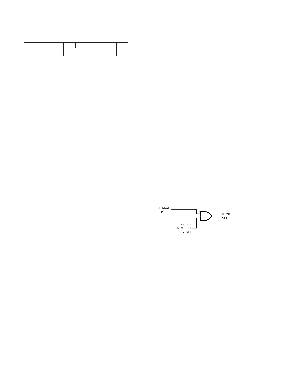
10.7 RESET
The device is initialized when the RESET pin is pulled low or
the On-chip Brownout Reset is activated. The Brownout
Reset feature is not available on the COP8SDR9.
10138911
FIGURE 8. Reset Logic
The following occurs upon initialization:
Port A: TRI-STATE (High Impedance Input)
Port B: TRI-STATE (High Impedance Input)
Port C: TRI-STATE (High Impedance Input)
Port D: HIGH
Port E: TRI-STATE (High Impedance Input)
Port F: TRI-STATE (High Impedance Input)
Port G: TRI-STATE (High Impedance Input)
Exceptions: If Watchdog is enabled, then G1 is Watchdog output. G0 and G2 have their weak pull-up en-
abled during RESET.
Port L: TRI-STATE (High Impedance Input)
PC: CLEARED to 0000
PSW, CNTRL and ICNTRL registers: CLEARED
SIOR:
UNAFFECTED after RESET with power already applied
www.national.com21
Page 22

10.0 Functional Description
(Continued)
RANDOM after RESET at power-on
T2CNTRL: CLEARED
T3CNTRL: CLEARED
HSTCR: CLEARED
ITMR: Cleared except Bit 6 (HSON) = 1
Accumulator, Timer 1, Timer 2 and Timer 3:
RANDOM after RESET
WKEN, WKEDG: CLEARED
WKPND: RANDOM
COP8SBR9/COP8SCR9/COP8SDR9
SP (Stack Pointer):
Initialized to RAM address 06F Hex
B and X Pointers:
UNAFFECTED after RESET with power already applied
RANDOM after RESET at power-on
S Register: CLEARED
RAM:
UNAFFECTED after RESET with power already applied
RANDOM after RESET at power-on
USART:
PSR, ENU, ENUR, ENUI: Cleared except the TBMT bit
which is set to one.
ISP CONTROL:
ISPADLO: CLEARED
ISPADHI: CLEARED
PGMTIM: PRESET TO VALUE FOR 10 MHz CKI
WATCHDOG (if enabled):
The device comes out of reset with both the WATCHDOG logic and the Clock Monitor detector armed, with
the WATCHDOG service window bits set and the
Clock Monitor bit set. The WATCHDOG and Clock
Monitor circuits are inhibited during reset. The
WATCHDOG service window bits being initialized high
default to the maximum WATCHDOG service window
of 64k T0 clock cycles. The Clock Monitor bit being
initialized high will cause a Clock Monitor error following reset if the clock has not reached the minimum
specified frequency at the termination of reset. A Clock
Monitor error will cause an active low error output on
pin G1. This error output will continue until 16–32 T0
clock cycles following the clock frequency reaching the
minimum specified value, at which time the G1 output
will go high.
10.7.1 External Reset
The RESET input when pulled low initializes the device. The
RESET pin must be held low for a minimum of one instruction cycle to guarantee a valid reset. During Power-Up ini-
tialization, the user must ensure that the RESET pin of a
device without the Brownout Reset feature is held low until
the device is within the specified V
edge on the RESET pin while V
voltage. Any rising
CC
is below the specified
CC
operating range may cause unpredictable results. An R/C
circuit on the RESET pin with a delay 5 times (5x) greater
than the power supply rise time is recommended. Reset
should also be wide enough to ensure crystal start-up upon
Power-Up.
RESET may also be used to cause an exit from the HALT
mode.
A recommended reset circuit for this device is shown in
Figure 9.
10138912
FIGURE 9. Reset Circuit Using External Reset
10.7.2 On-Chip Brownout Reset
When enabled, the device generates an internal reset as
rises. While VCCis less than the specified brownout
V
CC
voltage (V
the Idle Timer is preset with 00Fx (240–256 t
reaches a value greater than V
), the device is held in the reset condition and
bor
, the Idle Timer starts
bor
). When V
C
CC
counting down. Upon underflow of the Idle Timer, the internal
reset is released and the device will start executing instructions. This internal reset will perform the same functions as
external reset. Once V
is above the V
CC
and this initial Idle
bor
Timer time-out takes place, instruction execution begins and
the Idle Timer can be used normally. If, however, V
below the selected V
, an internal reset is generated, and
bor
CC
drops
the Idle Timer is preset with 00Fx. The device now waits until
is greater than V
V
CC
and the countdown starts over.
bor
When enabled, the functional operation of the device, at
frequency, is guaranteed down to the V
level.
bor
One exception to the above is that the brownout circuit will
insert a delay of approximately 3 ms on power up or any time
the V
drops below a voltage of about 1.8V. The device will
CC
be held in Reset for the duration of this delay before the Idle
Timer starts counting the 240 to 256 t
soon as the V
rises above the trigger voltage (approxi-
CC
. This delay starts as
C
mately 1.8V). This behavior is shown in Figure 10.
www.national.com 22
Page 23

10.0 Functional Description (Continued)
COP8SBR9/COP8SCR9/COP8SDR9
10138913
FIGURE 10. Brownout Reset Operation
In Case 1, V
rises from 0V and the on-chip RESET is
CC
undefined until the supply is greater than approximately
1.0V. At this time the brownout circuit becomes active and
holds the device in RESET. As the supply passes a level of
about 1.8V, a delay of about 3 ms (t
) is started and the Idle
d
Timer is preset to a value between 00F0 and 00FF (hex).
Once V
is greater than V
CC
Timer is allowed to count down (t
and tdhas expired, the Idle
bor
).
id
Case 2 shows a subsequent dip in the supply voltage which
goes below the approximate 1.8V level. As V
, the internal RESET signal is asserted. When VCCrises
V
bor
back above the 1.8V level, t
supply rise time is longer for this case, t
rises above V
V
CC
greater than V
and tidstarts immediately when VCCis
bor
.
bor
is started. Since the power
d
d
Case 3 shows a dip in the supply where V
, but not below 1.8V. On-chip RESET is asserted when
V
bor
goes below V
V
CC
goes back above V
and tidstarts as soon as the supply
bor
.
bor
drops below
CC
has expired before
drops below
CC
If the Brownout Reset feature is enabled, the internal reset
will not be turned off until the Idle Timer underflows. The
internal reset will perform the same functions as external
reset. The device is guaranteed to operate at the specified
frequency down to the specified brownout voltage. After the
underflow, the logic is designed such that no additional
internal resets occur as long as V
remains above the
CC
brownout voltage.
The device is relatively immune to short duration negative-
going V
filtering of V
transients (glitches). It is essential that good
CC
be done to ensure that the brownout feature
CC
works correctly. Power supply decoupling is vital even in
battery powered systems.
There are two optional brownout voltages. The part numbers
for the three versions of this device are:
COP8SBR9, V
= low voltage range
bor
COP8SCR9, V
= high voltage range
bor
COP8SDR9, BOR is disabled.
Refer to the device specifications for the actual V
volt-
bor
ages.
High brownout voltage devices are guaranteed to operate at
10MHz down to the brownout voltage. Low brownout voltage
devices are guaranteed to operate at 3.33MHz down to the
brownout voltage. Devices are not guaranteed to operate
at 10MHz down to the low brownout voltage.
Under no circumstances should the RESET pin be allowed
to float. If the on-chip Brownout Reset feature is being used,
the RESET pin should be connected directly to V
CC
. The
RESET input may also be connected to an external pull-up
resistor or to other external circuitry. Any rising edge on the
RESET pin while V
is below the specified operating range
CC
may cause unpredictable results. The output of the brownout
reset detector will always preset the Idle Timer to a value
between 00F0 and 00FF (240 to 256 t
). At this time, the
C
internal reset will be generated.
If the BOR feature is disabled, then no internal resets are
generated and the Idle Timer will power-up with an unknown
value. In this case, the external RESET must be used. When
BOR is disabled, this on-chip circuitry is disabled and draws
no DC current.
The contents of data registers and RAM are unknown following the on-chip reset.
www.national.com23
Page 24

10.0 Functional Description
(Continued)
10138914
COP8SBR9/COP8SCR9/COP8SDR9
FIGURE 11. Reset Circuit Using Power-On Reset
10.8 OSCILLATOR CIRCUITS
The device has two crystal oscillators to facilitate low power
operation while maintaining throughput when required. Further information on the use of the two oscillators is found in
Section 7.0 Power Saving Features. The low speed oscillator
utilizes the L0 and L1 port pins. References in the following
text to CKI will also apply to L0 and references to G7/CKO
will also apply to L1.
10.8.1 Oscillator
CKI is the clock input while G7/CKO is the clock generator
output to the crystal. An on-chip bias resistor connected
between CKI and CKO is provided to reduce system part
count. The value of the resistor is in the range of 0.5M to 2M
(typically 1.0M). Table 2 shows the component values required for various standard crystal values. Resistor R2 is
on-chip, for the high speed oscillator, and is shown for
reference. Figure 12 shows the crystal oscillator connection
diagram. A ceramic resonator of the required frequency may
be used in place of a crystal if the accuracy requirements are
not quite as strict.
TABLE 2. Crystal Oscillator Configuration,
= 25˚C, VCC=5V
T
A
R1 (kΩ)R2(MΩ) C1 (pF) C2 (pF)
0 On Chip 18 18 10
0 On Chip 18 18 5
0 On Chip 18–36 18–36 1
5.6 On Chip 100 100–156 0.455
020
** **
CKI Freq.
(MHz)
32.768
*
kHz
*
Applies to connection to low speed oscillator on port pins L0 and L1 only.
**
See Note below.
The crystal and other oscillator components should be
placed in close proximity to the CKI and CKO pins to minimize printed circuit trace length.
The values for the external capacitors should be chosen to
obtain the manufacturer’s specified load capacitance for the
crystal when combined with the parasitic capacitance of the
trace, socket, and package (which can vary from 0 to 8 pF).
The guideline in choosing these capacitors is:
Manufacturer’s specified load cap = (C
C
parasitic
)/(C1+C2)+
1*C2
C2can be trimmed to obtain the desired frequency. C
should be less than or equal to C1.
Note: The low power design of the low speed oscillator
makes it extremely sensitive to board layout and load capacitance. The user should place the crystal and load capacitors within 1cm. of the device and must ensure that the
above equation for load capacitance is strictly followed. If
these conditions are not met, the application may have
problems with startup of the low speed oscillator.
TABLE 3. Startup Times
CKI Frequency Startup Time
10 MHz 1–10 ms
3.33 MHz 3–10 ms
1 MHz 3–20 ms
455 kHz 10–30 ms
32 kHz (low speed oscillator) 2– 5 sec
10.8.2 Clock Doubler
This device contains a frequency doubler that doubles the
frequency of the oscillator selected to operate the main
microcontroller core. The details of how to select either the
high speed oscillator or low speed oscillator are described in,
Power Saving Features. When the high speed oscillator
connected to CKI operates at 10 MHz, the internal clock
frequency is 20 MHz, resulting in an instruction cycle time of
0.5 µs. When the 32 kHz oscillator connected to L0 and L1 is
selected, the internal clock frequency is 64 kHz, resulting in
an instruction cycle of 152.6 µs. The output of the clock
doubler is called MCLK and is referenced in many places
within this document.
2
www.national.com 24
Page 25

10.0 Functional Description (Continued)
High Speed Oscillator Low Speed Oscillator
10138915
FIGURE 12. Crystal Oscillator
COP8SBR9/COP8SCR9/COP8SDR9
10138916
10.9 CONTROL REGISTERS
10.9.1 CNTRL Register (Address X'00EE)
T1C3 T1C2 T1C1 T1C0 MSEL IEDG SL1 SL0
Bit 7 Bit 0
The Timer1 (T1) and MICROWIRE/PLUS control register
contains the following bits:
T1C3 Timer T1 mode control bit
T1C2 Timer T1 mode control bit
T1C1 Timer T1 mode control bit
T1C0 Timer T1 Start/Stop control in timer
modes 1 and 2. T1 Underflow Interrupt
Pending Flag in timer mode 3
MSEL Selects G5 and G4 as MICROWIRE/PLUS
signals SK and SO respectively
IEDG External interrupt edge polarity select
(0 = Rising edge, 1 = Falling edge)
SL1 & SL0 Select the MICROWIRE/PLUS clock divide
by (00 = 2, 01 = 4, 1x = 8)
10.9.2 PSW Register (Address X'00EF)
HC C T1PNDA T1ENA EXPND BUSY EXEN GIE
Bit 7 Bit 0
The PSW register contains the following select bits:
HC Half Carry Flag
C Carry Flag
T1PNDA Timer T1 Interrupt Pending Flag (Autoreload RA
in mode 1, T1 Underflow in Mode 2, T1Acapture
edge in mode 3)
T1ENA Timer T1 Interrupt Enable for Timer Underflow
or T1A Input capture edge
EXPND External interrupt pending
BUSY MICROWIRE/PLUS busy shifting flag
EXEN Enable external interrupt
GIE Global interrupt enable (enables interrupts)
The Half-Carry flag is also affected by all the instructions that
affect the Carry flag. The SC (Set Carry) and R/C (Reset
Carry) instructions will respectively set or clear both the carry
flags. In addition to the SC and R/C instructions, ADC,
SUBC, RRC and RLC instructions affect the Carry and Half
Carry flags.
10.9.3 ICNTRL Register (Address X'00E8)
Unused LPEN T0PND T0EN µWPND µWEN T1PNDB T1ENB
Bit 7 Bit 0
The ICNTRL register contains the following bits:
LPEN L Port Interrupt Enable (Multi-Input
Wake-up/Interrupt)
T0PND Timer T0 Interrupt pending
T0EN Timer T0 Interrupt Enable (Bit 12 toggle)
µWPND MICROWIRE/PLUS interrupt pending
µWEN Enable MICROWIRE/PLUS interrupt
T1PNDB Timer T1 Interrupt Pending Flag for T1B capture
edge
T1ENB Timer T1 Interrupt Enable for T1B Input capture
edge
10.9.4 T2CNTRL Register (Address X'00C6)
T2C3 T2C2 T2C1 T2C0 T2PNDA T2ENA T2PNDB T2ENB
Bit 7 Bit 0
The T2CNTRL register contains the following bits:
T2C3 Timer T2 mode control bit
T2C2 Timer T2 mode control bit
T2C1 Timer T2 mode control bit
T2C0 Timer T2 Start/Stop control in timer
modes 1 and 2, Timer T2 Underflow Interrupt
Pending Flag in timer mode 3
T2PNDA Timer T2 Interrupt Pending Flag (Autoreload
RA in mode 1, T2 Underflow in mode 2, T2A
capture edge in mode 3)
T2ENA Timer T2 Interrupt Enable for Timer Underflow
or T2A Input capture edge
T2PNDB Timer T2 Interrupt Pending Flag for T2B cap-
ture edge
T2ENB Timer T2 Interrupt Enable for T2B Input capture
edge
www.national.com25
Page 26

10.0 Functional Description
(Continued)
10.9.5 T3CNTRL Register (Address X'00B6)
T3C3 T3C2 T3C1 T3C0 T3PNDA T3ENA T3PNDB T3ENB
Bit 7 Bit 0
The T3CNTRL register contains the following bits:
T3C3 Timer T3 mode control bit
T3C2 Timer T3 mode control bit
T3C1 Timer T3 mode control bit
T3C0 Timer T3 Start/Stop control in timer
modes 1 and 2, Timer T3 Underflow Interrupt
COP8SBR9/COP8SCR9/COP8SDR9
T3PNDA Timer T3 Interrupt Pending Flag (Autoreload
T3ENA Timer T3 Interrupt Enable for Timer Underflow
T3PNDB Timer T3 Interrupt Pending Flag for T3B cap-
T3ENB Timer T3 Interrupt Enable for T3B Input capture
Pending Flag in timer mode 3
RA in mode 1, T3 Underflow in mode 2, T3A
capture edge in mode 3)
or T3A Input capture edge
ture edge
edge
10.9.6 HSTCR Register (Address X'00AF)
Reserved T3HS T2HS
Bit 7 Bit 0
The HSTCR register contains the following bits:
T3HS Places Timer T3 in High Speed Mode.
T2HS Places Timer T2 in High Speed Mode.
10.9.7 ITMR Register (Address X'00CF)
LSON HSON DCEN
Bit 7 Bit 0
CCKS
RSVD ITSEL2 ITSEL1 ITSEL0
EL
The ITMR register contains the following bits:
LSON Turns the low speed oscillator on or off.
HSON Turns the high speed oscillator on or off.
DCEN Selects the high speed oscillator or the low
speed oscillator as the Idle Timer Clock.
CCKSEL Selects the high speed oscillator or the low
speed oscillator as the primary CPU clock.
RSVD This bit is reserved and must be 0.
ITSEL2 Idle Timer period select bit.
ITSEL1 Idle Timer period select bit.
ITSEL0 Idle Timer period select bit.
www.national.com 26
Page 27

11.0 In-System Programming
11.1 INTRODUCTION
This device provides the capability to program the program
memory while installed in an application board. This feature
is called In System Programming (ISP). It provides a means
of ISP by using the MICROWIRE/PLUS, or the user can
provide his own, customized ISP routine. The factory installed ISP uses the MICROWIRE/PLUS port. The user can
provide his own ISP routine that uses any of the capabilities
of the device, such as USART, parallel port, etc.
COP8SBR9/COP8SCR9/COP8SDR9
11.2 FUNCTIONAL DESCRIPTION
The organization of the ISP feature consists of the user flash
program memory, the factory boot ROM, and some registers
dedicated to performing the ISP function. See Figure 13 for
a simplified block diagram. The factory installed ISP that
uses MICROWIRE/PLUS is located in the Boot ROM. The
size of the Boot ROM is 1K bytes and also contains code to
facilitate in system emulation capability. If a user chooses to
write his own ISP routine, it must be located in the flash
program memory.
FIGURE 13. Block Diagram of ISP
As described in 10.5 OPTION REGISTER, there is a bit,
FLEX, that controls whether the device exits RESET executing from the flash memory or the Boot ROM. The user must
program the FLEX bit as appropriate for the application. In
the erased state, the FLEX bit = 0 and the device will
power-up executing from Boot ROM. When FLEX = 0, this
assumes that either the MICROWIRE/PLUS ISP routine or
external programming is being used to program the device. If
using the MICROWIRE/PLUS ISP routine, the software in
the boot ROM will monitor the MICROWIRE/PLUS for commands to program the flash memory. When programming
the flash program memory is complete, the FLEX bit will
have to be programmed to a 1 and the device will have to be
reset, either by pulling external Reset to ground or by a
MICROWIRE/PLUS ISP EXIT command, before execution
from flash program memory will occur.
If FLEX = 1, upon exiting Reset, the device will begin executing from location 0000 in the flash program memory. The
assumption, here, is that either the application is not using
ISP, is using MICROWIRE/PLUS ISP by jumping to it within
the application code, or is using a customized ISP routine. If
a customized ISP routine is being used, then it must be
programmed into the flash memory by means of the
MICROWIRE/PLUS ISP or external programming as described in the preceding paragraph.
11.3 REGISTERS
There are six registers required to support ISP: Address
Register Hi byte (ISPADHI), Address Register Low byte
(ISPADLO), Read Data Register (ISPRD), Write Data Register (ISPWR), Write Timing Register (PGMTIM), and the
Control Register (ISPCNTRL). The ISPCNTRL Register is
not available to the user.
10138917
11.3.1 ISP Address Registers
The address registers (ISPADHI & ISPADLO) are used to
specify the address of the byte of data being written or read.
For page erase operations, the address of the beginning of
the page should be loaded. For mass erase operations,
0000 must be placed into the address registers. When reading the Option register, FFFF (hex) should be placed into the
address registers. Registers ISPADHI and ISPADLO are
cleared to 00 on Reset. These registers can be loaded from
either flash program memory or Boot ROM and must be
maintained for the entire duration of the operation.
Note: The actual memory address of the Option Register is
7FFF (hex), however the MICROWIRE/PLUS ISP routines
require the address FFFF (hex) to be used to read the
Option Register when the Flash Memory is secured.
TABLE 4. High Byte of ISP Address
ISPADHI
Bit 7 Bit 6 Bit 5 Bit 4 Bit 3 Bit 2 Bit 1 Bit 0
Addr15 Addr14 Addr 13 Addr12 Addr11 Addr10 Addr9 Addr8
TABLE 5. Low Byte of ISP Address
ISPADLO
Bit 7 Bit 6 Bit 5 Bit 4 Bit 3 Bit 2 Bit 1 Bit 0
Addr7 Addr6 Addr5 Addr4 Addr3 Addr2 Addr1 Addr0
www.national.com27
Page 28

11.0 In-System Programming
(Continued)
11.3.2 ISP Read Data Register
The Read Data Register (ISPRD) contains the value read
back from a read operation. This register can be accessed
from either flash program memory or Boot ROM. This register is undefined on Reset.
TABLE 6. ISP Read Data Register
ISPRD
Bit 7 Bit 6 Bit 5 Bit 4 Bit 3 Bit 2 Bit 1 Bit 0
Bit7 Bit6 Bit5 Bit4 Bit3 Bit2 Bit1 Bit0
COP8SBR9/COP8SCR9/COP8SDR9
11.3.3 ISP Write Data Register
The Write Data Register (ISPWR) contains the data to be
written into the specified address. This register is undetermined on Reset. This register can be accessed from either
flash program memory or Boot ROM. The Write Data register
must be maintained for the entire duration of the operation.
TABLE 7. ISP Write Data Register
ISPWR
Bit 7 Bit 6 Bit 5 Bit 4 Bit 3 Bit 2 Bit 1 Bit 0
Bit7 Bit6 Bit5 Bit4 Bit3 Bit2 Bit1 Bit0
11.3.4 ISP Write Timing Register
The Write Timing Register (PGMTIM) is used to control the
width of the timing pulses for write and erase operations. The
value to be written into this register is dependent on the
frequency of CKI and is shown in Table 8. This register must
be written before any write or erase operation can take
place. It only needs to be loaded once, for each value of CKI
frequency. This register can be loaded from either flash
program memory or Boot ROM and must be maintained for
the entire duration of the operation. The MICROWIRE/PLUS
ISP routine that is resident in the boot ROM requires that this
Register be defined prior to any access to the Flash memory.
Refer to 11.7 MICROWIRE/PLUS ISP for more information
on available ISP commands. On Reset, the PGMTIM register is loaded with the value that corresponds to 10 MHz
frequency for CKI.
TABLE 8. PGMTIM Register Format
PGMTIM
Register Bit CKI Frequency Range
76543210
0000000125kHz–33.3 kHz
0000001037.5 kHz–50 kHz
0000001150kHz–66.67 kHz
0000010062.5 kHz–83.3 kHz
00000101 75kHz–100kHz
00000111100kHz–133kHz
00001000112.5 kHz–150 kHz
00001011150kHz–200kHz
00001111200kHz–266.67 kHz
00010001225kHz–300kHz
00010111300kHz–400kHz
00011101375kHz–500kHz
00100111500kHz–666.67 kHz
00101111600kHz–800kHz
00111111800kHz–1.067 MHz
010001111MHz–1.33 MHz
010010001.125 MHz–1.5 MHz
01001011 1.5MHz–2MHz
010011112MHz–2.67 MHz
010101002.625 MHz–3.5 MHz
010110113.5MHz–4.67 MHz
01100011 4.5MHz–6MHz
01101111 6MHz–8MHz
011110117.5MHz–10MHz
R R/W R/W R/W R/W R/W R/W R/W
www.national.com 28
Page 29

11.0 In-System Programming
(Continued)
11.4 MANEUVERING BACK AND FORTH BETWEEN FLASH MEMORY AND BOOT ROM
When using ISP, at some point, it will be necessary to
maneuver between the flash program memory and the Boot
ROM, even when using customized ISP routines. This is
because it’s not possible to execute from the flash program
memory while it’s being programmed.
Two instructions are available to perform the jumping back
and forth: Jump to Boot (JSRB) and Return to Flash (RETF).
The JSRB instruction is used to jump from flash memory to
Boot ROM, and the RETF is used to return from the Boot
ROM back to the flash program memory. See 19.0 Instruc-
tion Set for specific details on the operation of these instructions.
The JSRB instruction must be used in conjunction with the
Key register. This is to prevent jumping to the Boot ROM in
the event of run-away software. For the JSRB instruction to
actually jump to the Boot ROM, the Key bit must be set. This
is done by writing the value shown in Table 9 to the Key
register. The Key is a 6 bit key and if the key matches, the
KEY bit will be set for 8 instruction cycles. The JSRB instruction must be executed while the KEY bit is set. If the KEY
does not match, then the KEY bit will not be set and the
JSRB will jump to the specified location in the flash memory.
In emulation mode, if a breakpoint is encountered while the
KEY is set, the counter that counts the instruction cycles will
be frozen until the breakpoint condition is cleared. If an
interrupt occurs while the key is set, the key will expire
before interrupt service is complete. It is recommended that
the software globally disable interrupts before setting the
key. The Key register is a memory mapped register. Its
format when writing is shown in Table 9. In normal operation,
it is not necessary to test the KEY bit before using the JSRB
instruction. The additional instructions required to test the
key may cause the key to time-out before the JSRB can be
executed.
TABLE 9. KEY Register Write Format
KEY When Writing
Bit 7 Bit 6 Bit 5 Bit 4 Bit 3 Bit 2 Bit 1 Bit 0
10 0 1 1 0 X X
Bits 7– 2: Key value that must be written to set the KEY bit.
Bits 1– 0: Don’t care.
11.5 FORCED EXECUTION FROM BOOT ROM
When the user is developing a customized ISP routine, code
lockups due to software errors may be encountered. The
normal, and preferred, method to recover from these conditions is to reprogram the device with the corrected code by
either an external parallel programmer or the emulation
tools. As a last resort, when this equipment is not available,
there is a hardware method to get out of these lockups and
force execution from the Boot ROM MICROWIRE/PLUS
routine. The customer will then be able to erase the Flash
Memory code and start over.
The method to force this condition is to drive the G6 pin to
high voltage (2 x V
condition on G6 must not be applied before V
stable, and must be held for at least 3 instruction cycles
longer than Reset is active. This special condition will bypass checking the state of the Flex bit in the Option Register
) and activate Reset. The high voltage
CC
is valid and
CC
and will start execution from location 0000 in the Boot ROM.
In this state, the user can input the appropriate commands,
using MICROWIRE/PLUS, to erase the flash program
memory and reprogram it. If the device is subsequently reset
before the Flex bit has been erased by specific Page Erase
or Mass Erase ISP commands, execution will start from
location 0000 in the Flash program memory. The high voltage (2 x V
) on G6 will not erase either the Flex or the
CC
Security bit in the Option Register. The Security bit, if set,
can only be erased by a Mass Erase of the entire contents of
the Flash Memory unless under the control of User ISP
routines in the Application Program.
While the G6 pin is at high voltage, the Load Clock will be
output onto G5, which will look like an SK clock to the
MICROWIRE/PLUS routine executing in slave mode. However, when G6 is at high voltage, the G6 input will also look
like a logic 1. The MICROWIRE/PLUS routine in Boot ROM
monitors the G6 input, waits for it to go low, debounces it,
and then enables the ISP routine. CAUTION: The Load clock
on G5 could be in conflict with the user’s external SK. It is up
to the user to resolve this conflict, as this condition is considered a minor issue that’s only encountered during software development. The user should also be cautious of
the high voltage applied to the G6 pin. This high voltage
could damage other circuitry connected to the G6 pin
(e.g. the parallel port of a PC). The user may wish to
disconnect other circuitry while G6 is connected to the high
voltage.
must be valid and stable before high voltage is applied
V
CC
to G6.
The correct sequence to be used to force execution from
Boot ROM is :
1. Disconnect G6 from the source of data for MICROWIRE/
PLUS ISP.
2. Apply V
to the device.
CC
3. Pull RESET Low.
4. After V
2xV
is valid and stable, connect a voltage between
CC
and VCC+7V to the G6 pin. Ensure that the rise
CC
time of the high voltage on G6 is slower than the minimum in the Electrical Specifications. Figure 14 shows a
possible circuit dliagram for implementing the2xV
CC
Be aware of the typical input current on the G6 pin when
the high voltage is applied. The resistor used in the RC
network, and the high voltage used, should be chosen to
keep the high voltage at the G6 pin between2xV
+7V.
V
CC
and
CC
5. Pull RESET High.
6. After a delay of at least three instruction cycles, remove
the high voltage from G6.
10138966
FIGURE 14. Circuit Diagram for Implementing the 2 x
V
CC
COP8SBR9/COP8SCR9/COP8SDR9
.
www.national.com29
Page 30

11.0 In-System Programming
(Continued)
11.6 RETURN TO FLASH MEMORY WITHOUT HARDWARE RESET
After programming the entire program memory, including
options, it is necessary to exit the Boot ROM and return to
the flash program memory for program execution. Upon
receipt and completion of the EXIT command through the
MICROWIRE/PLUS ISP, the ISP code will reset the part and
begin execution from the flash program memory as described in the Reset section. This assumes that the FLEX bit
in the Option register was programmed to 1.
11.7 MICROWIRE/PLUS ISP
COP8SBR9/COP8SCR9/COP8SDR9
National Semiconductor provides a program, which is available from our web site at www.national.com/cop8, that is
capable of programming a device from the parallel port of a
PC. The software accepts manually input commands and is
capable of downloading standard Intel HEX Format files.
Users who wish to write their own MICROWIRE/PLUS ISP
host software should refer to the COP8 FLASH ISP User
TABLE 10. MICROWIRE/PLUS ISP Commands
Command Function
PGMTIM_SET Write Pulse Timing
Register
PAGE_ERASE Page Erase 0xB3 Starting Address of
MASS_ERASE Mass Erase 0xBF Confirmation Code N/A (The entire Flash
READ_BYTE Read Byte 0x1D Address High, Address
BLOCKR Block Read 0xA3 Address High, Address
WRITE_BYTE Write Byte 0x71 Address High, Address
BLOCKW Block Write 0x8F Address High, Address
EXIT EXIT 0xD3 N/A N/A (Device will Reset)
INVALID N/A Any other invalid
Note: The user must ensure that Block Writes do not cross a 64 byte boundary within one operation.
11.8 USER ISP AND VIRTUAL E
The following commands will support transferring blocks of
data from RAM to flash program memory, and vice-versa.
The user is expected to enforce application security in this
case.
2
Command
Value (Hex)
Manual, available from the same web site. This document
includes details of command format and delays necessary
between command bytes.
The MICROWIRE/PLUS ISP supports the following features
and commands:
Write a value to the ISP Write Timing Register. NOTE:
•
This must be the first command after entering
MICROWIRE/PLUS ISP mode.
Erase the entire flash program memory (mass erase).
•
Erase a page at a specified address.
•
Read Option register.
•
Read a byte from a specified address.
•
Write a byte to a specified address.
•
Read multiple bytes starting at a specified address.
•
Write multiple bytes starting at a specified address.
•
Exit ISP and return execution to flash program memory.
•
The following table lists the MICROWIRE/PLUS ISP commands and provides information on required parameters and
return values.
Parameters Return Data
0x3B Value N/A
N/A
Page
Memory will be erased)
Data Byte if Security not
Low
Low, Byte Count (n)
High, Byte Count (n)
Low
0 ≤ n ≤ 32767
Low, Data Byte
Low, Byte Count (0 ≤ n
≤ 16), n Data Bytes
command will be
ignored
Erase the entire flash program memory (mass erase).
•
NOTE: Execution of this command will force the device
into the MICROWIRE/PLUS ISP mode.
Erase a page of flash memory at a specified address.
•
Read a byte from a specified address.
•
Write a byte to a specified address.
•
set. 0xFF if Security set.
Option Register if address
= 0xFFFF, regardless of
Security
n Data Bytes if Security
not set.
n Bytes of 0xFF if
Security set.
N/A
N/A
N/A
www.national.com 30
Page 31

11.0 In-System Programming
(Continued)
Copy a block of data from RAM into flash program
•
memory.
Copy a block of data from program flash memory to RAM.
•
The following table lists the User ISP/Virtual E
2
commands,
mand entry point is used as an argument to the JSRB
instruction. Table 12 lists the Ram locations and Peripheral
Registers, used for User ISP and Virtual E
pected contents. Please refer to the COP8 FLASH ISP User
Manual for additional information and programming examples on the use of User ISP and Virtual E
required parameters and return data, if applicable. The com-
TABLE 11. User ISP/Virtual E
Command/
Label
Function
Command
Entry Point
Parameters Return Data
cpgerase Page Erase 0x17 Register ISPADHI is loaded by the user
with the high byte of the address.
2
Entry Points
N/A (A page of memory beginning at
ISPADHI, ISPADLO will be erased)
Register ISPADLO is loaded by the
user with the low byte of the address.
cmserase Mass Erase 0x1A Accumulator A contains the
confirmation key 0x55.
creadbf Read Byte 0x11 Register ISPADHI is loaded by the user
N/A (The entire Flash Memory will be
erased)
Data Byte in Register ISPRD.
with the high byte of the address.
Register ISPADLO is loaded by the
user with the low byte of the address.
cblockr Block Read 0x26 Register ISPADHI is loaded by the user
with the high byte of the address.
Register ISPADLO is loaded by the
n Data Bytes, Data will be returned
beginning at a location pointed to by
the RAM address in X.
user with the low byte of the address.
X pointer contains the beginning RAM
address where the result(s) will be
returned.
Register BYTECOUNTLO contains the
number of n bytes to read
(0 ≤ n ≤ 255). It is up to the user to
setup the segment register.
cwritebf Write Byte 0x14 Register ISPADHI is loaded by the user
N/A
with the high byte of the address.
Register ISPADLO is loaded by the
user with the low byte of the address.
Register ISPWR contains the Data
Byte to be written.
cblockw Block Write 0x23 Register ISPADHI is loaded by the user
N/A
with the high byte of the address.
Register ISPADLO is loaded by the
user with the low byte of the address.
Register BYTECOUNTLO contains the
number of n bytes to write (0 ≤ n ≤ 16).
The combination of the
BYTECOUNTLO and the ISPADLO
registers must be set such that the
operation will not cross a 64 byte
boundary.
X pointer contains the beginning RAM
address of the data to be written.
It is up to the user to setup the
segment register.
exit EXIT 0x62 N/A N/A (Device will Reset)
2
, and their ex-
2
.
COP8SBR9/COP8SCR9/COP8SDR9
www.national.com31
Page 32

11.0 In-System Programming (Continued)
2
TABLE 11. User ISP/Virtual E
Command/
Label
uwisp MICROWIRE/
COP8SBR9/COP8SCR9/COP8SDR9
Register
ISPADHI High byte of Flash Memory Address 0xA9
ISPADLO Low byte of Flash Memory Address 0xA8
ISPWR The user must store the byte to be written into this register before jumping into the
ISPRD Data will be returned to this register after the read byte routine execution. 0xAA
ISPKEY The ISPKEY Register is required to validate the JSRB instruction and must be loaded
BYTECOUNTLO Holds the count of the number of bytes to be read or written in block operations. 0xF1
PGMTIM Write Timing Register. This register must be loaded, by the user, with the proper value
Confirmation Code The user must place this code in the accumulator before execution of a Flash Memory
KEY Must be transferred to the ISPKEY register before execution of a JSRB instruction. 0x98
Function
PLUS
ISP Start
Name
Command
Entry Point
0x00 N/A N/A (Device will be in
TABLE 12. Register and Bit Name Definitions
write byte routine.
within 6 instruction cycles before the JSRB.
before execution of any USER ISP Write or Erase operation. Refer to Table 8 for the
correct value.
Mass Erase command.
Entry Points (Continued)
Parameters Return Data
MICROWIRE/PLUS ISP Mode. Must be
terminated by MICROWIRE/PLUS ISP
EXIT command which will Reset the
device)
Purpose
RAM
Location
0xAB
0xE2
0xE1
A
11.9 RESTRICTIONS ON SOFTWARE WHEN CALLING ISP ROUTINES IN BOOT ROM
1. The hardware will disable interrupts from occurring. The
hardware will leave the GIE bit in its current state, and if
set, the hardware interrupts will occur when execution is
returned to Flash Memory. Subsequent interrupts, during ISP operation, from the same interrupt source will be
lost. Interrupts may occur between setting the KEY
and executing the JSRB instruction. In this case, the
KEY will expire before the JSRB is executed. It is,
therefore, recommended that the software globally
disable interrupts before setting the Key.
2. The security feature in the MICROWIRE/PLUS ISP is
guaranteed by software and not hardware. When executing the MICROWIRE/PLUS ISP routine, the security
bit is checked prior to performing all instructions. Only
the mass erase command, write PGMTIM register, and
reading the Option register is permitted within the
MICROWIRE/PLUS ISP routine. When the user is performing his own ISP, all commands are permitted. The
entry points from the user’s ISP code do not check for
security. It is the burden of the user to guarantee his own
security. See the Security bit description in 10.5 OPTION
REGISTER for more details on security.
3. When using any of the ISP functions in Boot ROM, the
ISP routines will service the WATCHDOG within the
selected upper window. Upon return to flash memory,
the WATCHDOG is serviced, the lower window is enabled, and the user can service the WATCHDOG anytime following exit from Boot ROM, but must service it
within the selected upper window to avoid a WATCHDOG error.
4. Block Writes can start anywhere in the page of Flash
memory, but cannot cross half page or full page boundaries.
5. The user must ensure that a page erase or a mass
erase is executed between two consecutive writes to
the same location in Flash memory. Two writes to
the same location without an intervening erase will
produce unpredicatable results including possible
disturbance of unassociated locations.
11.10 FLASH MEMORY DURABILITY CONSIDERATIONS
The endurance of the Flash Memory (number of possible
Erase/Write cycles) is a function of the erase time and the
lowest temperature at which the erasure occurs. If the device
is to be used at low temperature, additional erase operations
can be used to extend the erase time. The user can determine how many times to erase a page based on what
endurance is desired for the application (e.g. four page
erase cycles, each time a page erase is done, may be
required to achieve the typical 100k Erase/Write cycles in an
application which may be operating down to 0˚C). Also, the
customer can verify that the entire page is erased, with
software, and request additional erase operations if desired.
www.national.com 32
Page 33

COP8SBR9/COP8SCR9/COP8SDR9
11.0 In-System Programming
(Continued)
TABLE 13. Typical Flash Memory Endurance
Low End of Operating Temp Range
Erase
Time
1 ms 60k 60k 60k 100k 100k
2 ms 60k 60k 60k 100k 100k
3 ms 60k 60k 60k 100k 100k
−40˚C −20˚C 0˚C 25˚C
>
25˚C
Low End of Operating Temp Range
Erase
Time
4 ms 60k 60k 100k 100k 100k
5 ms 70k 70k 100k 100k 100k
6 ms 80k 80k 100k 100k 100k
7 ms 90k 90k 100k 100k 100k
8 ms 100k 100k 100k 100k 100k
−40˚C −20˚C 0˚C 25˚C
>
25˚C
www.national.com33
Page 34

12.0 Timers
The device contains a very versatile set of timers (T0, T1, T2
and T3). Timers T1, T2 and T3 and associated autoreload/
capture registers power up containing random data.
12.1 TIMER T0 (IDLE TIMER)
The device supports applications that require maintaining
real time and low power with the IDLE mode. This IDLE
mode support is furnished by the IDLE Timer T0, which is a
16-bit timer. The user cannot read or write to the IDLE Timer
T0, which is a count down timer.
As described in 13.0 Power Saving Features, the clock to the
IDLE Timer depends on which mode the device is in. If the
device is in High Speed mode, the clock to the IDLE Timer is
COP8SBR9/COP8SCR9/COP8SDR9
the instruction cycle clock (one-fifth of the CKI frequency). If
the device is in Dual Clock mode or Low Speed mode, the
clock to the IDLE Timer is the 32 kHz clock. For the remainder of this section, the term “selected clock” will refer to the
clock selected by the Power Save mode of the device.
During Dual Clock and Low Speed modes, the divide by 10
that creates the instruction cycle clock is disabled, to minimize power consumption.
In addition to its time base function, the Timer T0 supports
the following functions:
Exit out of the Idle Mode (See Idle Mode description)
•
WATCHDOG logic (See WATCHDOG description)
•
Start up delay out of the HALT mode
•
Start up delay from BOR
•
Figure 15 is a functional block diagram showing the structure
of the IDLE Timer and its associated interrupt logic.
Bits 11 through 15 of the ITMR register can be selected for
triggering the IDLE Timer interrupt. Each time the selected
bit underflows (every 4k, 8k, 16k, 32k or 64k selected
clocks), the IDLE Timer interrupt pending bit T0PND is set,
thus generating an interrupt (if enabled), and bit 6 of the Port
G data register is reset, thus causing an exit from the IDLE
mode if the device is in that mode.
In order for an interrupt to be generated, the IDLE Timer
interrupt enable bit T0EN must be set, and the GIE (Global
Interrupt Enable) bit must also be set. The T0PND flag and
T0EN bit are bits 5 and 4 of the ICNTRL register, respectively. The interrupt can be used for any purpose. Typically, it
is used to perform a task upon exit from the IDLE mode. For
more information on the IDLE mode, refer to 13.0 Power
Saving Features.
The Idle Timer period is selected by bits 0–2 of the ITMR
register Bit 3 of the ITMR Register is reserved and should
not be used as a software flag. Bits 4 through 7 of the ITMR
Register are used by the dual clock and are described in
13.0 Power Saving Features.
FIGURE 15. Functional Block Diagram for Idle Timer T0
TABLE 14. Idle Timer Window Length
Idle Timer Period
ITSEL2 ITSEL1 ITSEL0
0 0 0 4,096 inst.
0 0 1 8,192 inst.
0 1 0 16,384 inst.
0 1 1 32,768 inst.
1 0 0 65,536 inst.
1 0 1 Reserved - Undefined
www.national.com 34
High Speed
Mode
cycles
cycles
cycles
cycles
cycles
Dual Clock
or
Low Speed
Mode
0.125
seconds
0.25 seconds
0.5 seconds
1 second
2 seconds
10138918
Idle Timer Period
ITSEL2 ITSEL1 ITSEL0
1 1 0 Reserved - Undefined
1 1 1 Reserved - Undefined
High Speed
Mode
Dual Clock
or
Low Speed
Mode
The ITSEL bits of the ITMR register are cleared on Reset
and the Idle Timer period is reset to 4,096 instruction cycles.
12.1.1 ITMR Register
LSON HSON DCEN
Bit 7 Bit 6 Bit 5 Bit 4 Bit 3 Bit 2 Bit 1 Bit 0
CCK
RSVD ITSEL2 ITSEL1 ITSEL0
SEL
Bits 7– 4: Described in 13.0 Power Saving Features.
Page 35

12.0 Timers (Continued)
Note: Documentation for previous COP8 devices, which included the Programmable Idle Timer, recommended the user
write zero to the high order bits of the ITMR Register. If
existing programs are updated to use this device, writing
zero to these bits will cause the device to reset (see 13.0
Power Saving Features).
RSVD: This bit is reserved and must be set to 0.
ITSEL2:0: Selects the Idle Timer period as described in
Table 14, Idle Timer Window Length.
Any time the IDLE Timer period is changed there is the
possibility of generating a spurious IDLE Timer interrupt by
setting the T0PND bit. The user is advised to disable IDLE
Timer interrupts prior to changing the value of the ITSEL bits
of the ITMR Register and then clear the T0PND bit before
attempting to synchronize operation to the IDLE Timer.
12.2 TIMER T1, TIMER T2, AND TIMER T3
The device has a set of three powerful timer/counter blocks,
T1, T2, and T3. Since T1, T2 and T3 are identical, except for
the high speed operation of T2 and T3, all comments are
equally applicable to any of the three timer blocks which will
be referred to as Tx. Differences between the timers will be
specifically noted.
Each timer block consists of a 16-bit timer, Tx, and two
supporting 16-bit autoreload/capture registers, RxA and
RxB. Each timer block has two pins associated with it, TxA
and TxB. The pin TxA supports I/O required by the timer
block, while the pin TxB is an input to the timer block. The
timer block has three operating modes: Processor Independent PWM mode, External Event Counter mode, and Input
Capture mode.
The control bits TxC3, TxC2, and TxC1 allow selection of the
different modes of operation.
12.2.1 Timer Operating Speeds
Each of the Tx timers, except T1, have the ability to operate
at either the instruction cycle frequency (low speed) or the
internal clock frequency (MCLK). For 10 MHz CKI, the instruction cycle frequency is 2 MHz and the internal clock
frequency is 20 MHz. This feature is controlled by the High
Speed Timer Control Register, HSTCR. Its format is shown
below. To place a timer, Tx, in high speed mode, set the
appropriate TxHS bit to 1. For low speed operation, clear the
appropriate TxHS bit to 0. This register is cleared to 00 on
Reset.
HSTCR
Bit 7 Bit 6 Bit 5 Bit 4 Bit 3 Bit 2
000000T3HS T2HS
Bit1Bit
0
a microcontroller that has only a single reload register requires an additional software to update the reload value
(alternate between the on-time/off-time).
The timer can generate the PWM output with the width and
duty cycle controlled by the values stored in the reload
registers. The reload registers control the countdown values
and the reload values are automatically written into the timer
when it counts down through 0, generating interrupt on each
reload. Under software control and with minimal overhead,
the PWM outputs are useful in controlling motors, triacs, the
intensity of displays, and in providing inputs for data acquisition and sine wave generators.
In this mode, the timer Tx counts down at a fixed rate of t
(T2 and T3 may be selected to operate from MCLK). Upon
every underflow the timer is alternately reloaded with the
contents of supporting registers, RxA and RxB. The very first
underflow of the timer causes the timer to reload from the
register RxA. Subsequent underflows cause the timer to be
reloaded from the registers alternately beginning with the
register RxB.
Figure 16 shows a block diagram of the timer in PWM mode.
The underflows can be programmed to toggle the TxA output
pin. The underflows can also be programmed to generate
interrupts.
Underflows from the timer are alternately latched into two
pending flags, TxPNDA and TxPNDB. The user must reset
these pending flags under software control. Two control
enable flags, TxENA and TxENB, allow the interrupts from
the timer underflow to be enabled or disabled. Setting the
timer enable flag TxENA will cause an interrupt when a timer
underflow causes the RxA register to be reloaded into the
timer. Setting the timer enable flag TxENB will cause an
interrupt when a timer underflow causes the RxB register to
be reloaded into the timer. Resetting the timer enable flags
will disable the associated interrupts.
Either or both of the timer underflow interrupts may be
enabled. This gives the user the flexibility of interrupting
once per PWM period on either the rising or falling edge of
the PWM output. Alternatively, the user may choose to interrupt on both edges of the PWM output.
COP8SBR9/COP8SCR9/COP8SDR9
C
12.2.2 Mode 1. Processor Independent PWM Mode
One of the timer’s operating modes is the Processor Independent PWM mode. In this mode, the timers generate a
“Processor Independent” PWM signal because once the
timer is set up, no more action is required from the CPU
which translates to less software overhead and greater
throughput. The user software services the timer block only
when the PWM parameters require updating. This capability
is provided by the fact that the timer has two separate 16-bit
reload registers. One of the reload registers contains the
“ON” time while the other holds the “OFF” time. By contrast,
10138919
FIGURE 16. Timer in PWM Mode
www.national.com35
Page 36

12.0 Timers (Continued)
12.2.3 Mode 2. External Event Counter Mode
This mode is quite similar to the processor independent
PWM mode described above. The main difference is that the
timer, Tx, is clocked by the input signal from the TxA pin after
synchronization to the appropriate internal clock (t
MCLK). The Tx timer control bits, TxC3, TxC2 and TxC1
allow the timer to be clocked either on a positive or negative
edge from the TxA pin. Underflows from the timer are latched
into the TxPNDA pending flag. Setting the TxENA control flag
will cause an interrupt when the timer underflows.
In this mode the input pin TxB can be used as an independent positive edge sensitive interrupt input if the TxENB
control flag is set. The occurrence of a positive edge on the
COP8SBR9/COP8SCR9/COP8SDR9
TxB input pin is latched into the TxPNDB flag.
Figure 17 shows a block diagram of the timer in External
Event Counter mode.
Note: The PWM output is not available in this mode since the
TxA pin is being used as the counter input clock.
nization to the appropriate internal clock (t
or MCLK). Con-
C
trol bits, TxC3, TxC2 and TxC1, allow the trigger events to be
specified either as a positive or a negative edge. The trigger
condition for each input pin can be specified independently.
The trigger conditions can also be programmed to generate
interrupts. The occurrence of the specified trigger condition
or
C
on the TxA and TxB pins will be respectively latched into the
pending flags, TxPNDA and TxPNDB. The control flag
TxENA allows the interrupt on TxA to be either enabled or
disabled. Setting the TxENA flag enables interrupts to be
generated when the selected trigger condition occurs on the
TxA pin. Similarly, the flag TxENB controls the interrupts
from the TxB pin.
Underflows from the timer can also be programmed to generate interrupts. Underflows are latched into the timer TxC0
pending flag (the TxC0 control bit serves as the timer underflow interrupt pending flag in the Input Capture mode). Consequently, the TxC0 control bit should be reset when entering the Input Capture mode. The timer underflow interrupt is
enabled with the TxENA control flag. When a TxA interrupt
occurs in the Input Capture mode, the user must check both
the TxPNDA and TxC0 pending flags in order to determine
whether a TxA input capture or a timer underflow (or both)
caused the interrupt.
Figure 18 shows a block diagram of the timer T1 in Input
Capture mode. T2 and T3 are identical to T1.
10138920
FIGURE 17. Timer in External Event Counter Mode
12.2.4 Mode 3. Input Capture Mode
The device can precisely measure external frequencies or
time external events by placing the timer block, Tx, in the
input capture mode. In this mode, the reload registers serve
as independent capture registers, capturing the contents of
the timer when an external event occurs (transition on the
timer input pin). The capture registers can be read while
maintaining count, a feature that lets the user measure
elapsed time and time between events. By saving the timer
value when the external event occurs, the time of the external event is recorded. Most microcontrollers have a latency
time because they cannot determine the timer value when
the external event occurs. The capture register eliminates
the latency time, thereby allowing the applications program
to retrieve the timer value stored in the capture register.
In this mode, the timer Tx is constantly running at the fixed t
C
or MCLK rate. The two registers, RxA and RxB, act as
capture registers. Each register also acts in conjunction with
a pin. The register RxA acts in conjunction with the TxA pin
and the register RxB acts in conjunction with the TxB pin.
The timer value gets copied over into the register when a
trigger event occurs on its corresponding pin after synchro-
www.national.com 36
10138921
FIGURE 18. Timer in Input Capture Mode
12.3 TIMER CONTROL FLAGS
The control bits and their functions are summarized below.
TxC3 Timer mode control
TxC2 Timer mode control
TxC1 Timer mode control
TxC0 Timer Start/Stop control in Modes 1 and 2 (Pro-
cessor Independent PWM and External Event
Counter), where 1 = Start, 0 = Stop
Timer Underflow Interrupt Pending Flag in Mode
3 (Input Capture)
TxPNDA Timer Interrupt Pending Flag
TxENA Timer Interrupt Enable Flag
1 = Timer Interrupt Enabled
0 = Timer Interrupt Disabled
TxPNDB Timer Interrupt Pending Flag
Page 37

12.0 Timers (Continued)
TxENB Timer Interrupt Enable Flag
1 = Timer Interrupt Enabled
0 = Timer Interrupt Disabled
The timer mode control bits (TxC3, TxC2 and TxC1) are
detailed in Table 15, Timer Operating Modes.
When the high speed timers are counting in high speed
mode, directly altering the contents of the timer upper or
lower registers, the PWM outputs or the reload registers is
not recommended. Bit operations can be particularly prob-
TABLE 15. Timer Operating Modes
Mode TxC3 TxC2 TxC1 Description
1 0 1 PWM: TxA Toggle Autoreload RA Autoreload RB t
1
2
3
1 0 0 PWM: No TxA
Toggle
0 0 0 External Event
Counter
0 0 1 External Event
Counter
0 1 0 Captures: Pos. TxA Edge Pos. TxB Edge t
TxA Pos. Edge or Timer
TxB Pos. Edge Underflow
1 1 0 Captures: Pos. TxA Neg. TxB t
TxA Pos. Edge Edge or Timer Edge
TxB Neg. Edge Underflow
0 1 1 Captures: Neg. TxA Pos. TxB t
TxA Neg. Edge Edge or Timer Edge
TxB Pos. Edge Underflow
1 1 1 Captures: Neg. TxA Neg. TxB t
TxA Neg. Edge Edge or Timer Edge
TxB Neg. Edge Underflow
lematic. Since any of these six registers or the PWM outputs
can change as many as ten times in a single instruction
cycle, performing an SBIT or RBIT operation with the timer
running can produce unpredictable results. The recommended procedure is to stop the timer, perform any changes
to the timer, the PWM outputs or reload register values, and
then re-start the timer. This warning does not apply to the
timer control register. Any type of read/write operation, including SBIT and RBIT may be performed on this register in
any operating mode.
Interrupt A
Source
Autoreload RA Autoreload RB t
Interrupt B
Source
Timer
Counts On
or MCLK
C
or MCLK
C
Timer Underflow Pos. TxB Edge TxA Pos.
Edge
Timer Underflow Pos. TxB Edge TxA Neg.
Edge
or MCLK
C
or MCLK
C
or MCLK
C
or MCLK
C
COP8SBR9/COP8SCR9/COP8SDR9
13.0 Power Saving Features
Today, the proliferation of battery-operated applications has
placed new demands on designers to drive power consumption down. Battery operated systems are not the only type of
applications demanding low power. The power budget constraints are also imposed on those consumer/industrial applications where well regulated and expensive power supply
costs cannot be tolerated. Such applications rely on low cost
and low power supply voltage derived directly from the
“mains” by using voltage rectifier and passive components.
Low power is demanded even in automotive applications,
due to increased vehicle electronics content. This is required
to ease the burden from the car battery. Low power 8-bit
microcontrollers supply the smarts to control batteryoperated, consumer/industrial, and automotive applications.
The device offers system designers a variety of low-power
consumption features that enable them to meet the demanding requirements of today’s increasing range of low-power
applications. These features include low voltage operation,
low current drain, and power saving features such as HALT,
IDLE, and Multi-Input Wake-Up (MIWU).
This device supports three operating modes, each of which
have two power save modes of operation. The three operat-
ing modes are: High Speed, Dual Clock, and Low Speed.
Within each operating mode, the two power save modes are:
HALT and IDLE. In the HALT mode of operation, all microcontroller activities are stopped and power consumption is
reduced to a very low level. In this device, the HALT mode is
enabled and disabled by a bit in the Option register. The
IDLE mode is similar to the HALT mode, except that certain
sections of the device continue to operate, such as: the
on-board oscillator, the IDLE Timer (Timer T0), and the Clock
Monitor. This allows real time to be maintained. During
power save modes of operation, all on board RAM, registers,
I/O states and timers (with the exception of T0) are unaltered.
Two oscillators are used to support the three different operating modes. The high speed oscillator refers to the oscillator
connected to CKI and the low speed oscillator refers to the
32 kHz oscillator connected to pins L0 & L1. When using L0
and L1 for the low speed oscillator, the user must ensure that
the L0 and L1 pins are configured for hi-Z input, L1 is not
using CKX on the USART, and Multi-Input Wake-up for these
pins is disabled.
A diagram of the three modes is shown in Figure 19.
www.national.com37
Page 38

13.0 Power Saving Features (Continued)
COP8SBR9/COP8SCR9/COP8SDR9
FIGURE 19. Diagram of Power Save Modes
10138922
13.1 POWER SAVE MODE CONTROL REGISTER
The ITMR control register allows for navigation between the
three different modes of operation. It is also used for the Idle
Timer. The register bit assignments are shown below. This
register is cleared to 40 (hex) by Reset as shown below.
LSON HSON DCEN CCK
Bit 7 Bit 6 Bit 5 Bit 4 Bit 3 Bit 2 Bit 1 Bit 0
RSVD ITSEL2 ITSEL1 ITSEL0
SEL
LSON: This bit is used to turn-on the low-speed oscilla-
tor. When LSON = 0, the low speed oscillator is
off. When LSON = 1, the low speed oscillator is
on. There is a startup time associated with this
oscillator. See the Oscillator Circuits section.
HSON: This bit is used to turn-on the high speed oscil-
lator. When HSON = 0, the high speed oscillator
is off. When HSON = 1, the high speed oscillator
is on. There is a startup time associated with this
oscillator. See the startup time table in the Oscillator Circuits section.
DCEN: This bit selects the clock source for the Idle
Timer. If this bit = 0, then the high speed clock is
the clock source for the Idle Timer. If this bit = 1,
then the low speed clock is the clock source for
the Idle Timer. The low speed oscillator must be
started and stabilized before setting this bit to a
1.
CCKSEL: This bit selects whether the high speed clock or
low speed clock is gated to the microcontroller
core. When this bit = 0, the Core clock will be the
high speed clock. When this bit = 1, then the
Core clock will be the low speed clock. Before
switching this bit to either state, the appropriate
clock should be turned on and stabilized.
DCEN CCKSEL
0 0 High Speed Mode. Core and Idle Timer
Clock = High Speed
1 0 Dual Clock Mode. Core clock = High
Speed; Idle Timer = Low Speed
1 1 Low Speed Mode. Core and Idle Timer
Clock = Low Speed
0 1 Invalid. If this is detected, the Low
Speed Mode will be forced.
RSVD: This bit is reserved and must be 0.
Bits 2– 0: These are bits used to control the Idle Timer. See
12.1 TIMER T0 (IDLE TIMER) for the description
of these bits.
Table 16 lists the valid contents of the four most significant
bits of the ITMR Register. Any other value is illegal. States
are presented in the only valid sequence. Any attempt to
make a transition to any state other than an adjacent valid
state will be ignored by the logic and the ITMR Register will
not be changed.
TABLE 16. Valid Contents of Dual Clock Control Bits
LSON HSON DCEN CCKSEL Mode
0 1 0 0 High Speed
1 1 0 0 High Speed/Dual
Clock Transition
1 1 1 0 Dual Clock
1 1 1 1 Dual Clock/Low
Speed Transition
1 0 1 1 Low Speed
www.national.com 38
Page 39

13.0 Power Saving Features
(Continued)
13.2 OSCILLATOR STABILIZATION
Both the high speed oscillator and low speed oscillator have
a startup delay associated with them. When switching between the modes, the software must ensure that the appropriate oscillator is started up and stabilized before switching
to the new mode. See Table 3, Startup Times for approximate startup times for both oscillators.
13.3 HIGH SPEED MODE OPERATION
This mode of operation allows high speed operation for both
the main Core clock and also for the Idle Timer. This is the
default mode of the device and will always be entered upon
any of the Reset conditions described in the Reset section. It
can also be entered from Dual Clock mode. It cannot be
directly entered from the Low Speed mode without passing
through the Dual Clock mode first.
To enter from the Dual Clock mode, the following sequence
must be followed using two separate instructions:
1. Software clears DCEN to 0.
2. Software clears LSON to 0.
13.3.1 High Speed Halt Mode
The fully static architecture of this device allows the state of
the microcontroller to be frozen. This is accomplished by
stopping the internal clock of the device during the HALT
mode. The controller also stops the CKI pin from oscillating
during the HALT mode. The processor can be forced to exit
the HALT mode and resume normal operation at any time.
During normal operation, the actual power consumption depends heavily on the clock speed and operating voltage
used in an application and is shown in the Electrical Specifications. In the HALT mode, the device only draws a small
leakage current, plus current for the BOR feature (if enabled), plus any current necessary for driving the outputs.
Since total power consumption is affected by the amount of
current required to drive the outputs, all I/Os should be
configured to draw minimal current prior to entering the
HALT mode, if possible. In order to reduce power consumption even further, the power supply (V
a very low level during the HALT mode, just high enough to
guarantee retention of data stored in RAM. The allowed
lower voltage level (V
) is specified in the Electrical Specs
R
section.
13.3.1.1 Entering The High Speed Halt Mode
The device enters the HALT mode under software control
when the Port G data register bit 7 is set to 1. All processor
action stops in the middle of the next instruction cycle, and
power consumption is reduced to a very low level.
) can be reduced to
CC
COP8SBR9/COP8SCR9/COP8SDR9
13.3.1.3 HALT Exit Using Reset
A device Reset, which is invoked by a low-level signal on the
RESET input pin, takes the device out of the HALT mode
and starts execution from address 0000H. The initialization
software should determine what special action is needed, if
any, upon start-up of the device from HALT. The initialization
of all registers following a RESET exit from HALT is described in the Reset section of this manual.
13.3.1.4 HALT Exit Using Multi-Input Wake-up
The device can be brought out of the HALT mode by a
transition received on one of the available Wake-up pins.
The pins used and the types of transitions sensed on the
Multi-input pins are software programmable. For information
on programming and using the Multi-Input Wake-up feature,
refer to the Multi-Input Wake-up section.
A start-up delay is required between the device wake-up and
the execution of program instructions, depending on the type
of chip clock. The start-up delay is mandatory, and is implemented whether or not the CLKDLY bit is set. This is because all crystal oscillators and resonators require some
time to reach a stable frequency and full operating amplitude.
The IDLE Timer (Timer T0) provides a fixed delay from the
time the clock is enabled to the time the program execution
begins. Upon exit from the HALT mode, the IDLE Timer is
enabled with a starting value of 256 and is decremented with
each instruction cycle. (The instruction clock runs at one-fifth
the frequency of the high speed oscillator.) An internal
Schmitt trigger connected to the on-chip CKI inverter ensures that the IDLE Timer is clocked only when the oscillator
has a large enough amplitude. (The Schmitt trigger is not
part of the oscillator closed loop.) When the IDLE Timer
underflows, the clock signals are enabled on the chip, allowing program execution to proceed. Thus, the delay is equal
to 256 instruction cycles.
Note: To ensure accurate operation upon start-up of the
device using Multi-Input Wake-up, the instruction in the application program used for entering the HALT mode should
be followed by two consecutive NOP (no-operation) instructions.
13.3.1.5 Options
This device has two options associated with the HALT mode.
The first option enables the HALT mode feature, while the
second option disables HALT mode operation. Selecting the
disable HALT mode option will cause the microcontroller to
ignore any attempts to HALT the device under software
control. Note that this device can still be placed in the HALT
mode by stopping the clock input to the microcontroller, if the
program memory is masked ROM. See the Option section
for more details on this option bit.
13.3.1.2 Exiting The High Speed Halt Mode
There is a choice of methods for exiting the HALT mode: a
chip Reset using the RESET pin or a Multi-Input Wake-up.
www.national.com39
Page 40

13.0 Power Saving Features (Continued)
COP8SBR9/COP8SCR9/COP8SDR9
FIGURE 20. Wake-up from HALT
10138923
13.3.2 High Speed Idle Mode
In the IDLE mode, program execution stops and power
consumption is reduced to a very low level as with the HALT
mode. However, the high speed oscillator, IDLE Timer (Timer
T0), and Clock Monitor continue to operate, allowing real
time to be maintained. The device remains idle for a selected
amount of time up to 65,536 instruction cycles, or 32.768
milliseconds with a 2 MHz instruction clock frequency, and
then automatically exits the IDLE mode and returns to normal program execution.
The device is placed in the IDLE mode under software
control by setting the IDLE bit (bit 6 of the Port G data
register).
The IDLE Timer window is selectable from one of five values,
4k, 8k, 16k, 32k or 64k instruction cycles. Selection of this
value is made through the ITMR register.
The IDLE mode uses the on-chip IDLE Timer (Timer T0) to
keep track of elapsed time in the IDLE state. The IDLE Timer
runs continuously at the instruction clock rate, whether or not
the device is in the IDLE mode. Each time the bit of the timer
associated with the selected window toggles, the T0PND bit
is set, an interrupt is generated (if enabled), and the device
exits the IDLE mode if in that mode. If the IDLE Timer
interrupt is enabled, the interrupt is serviced before execution of the main program resumes. (However, the instruction
which was started as the part entered the IDLE mode is
completed before the interrupt is serviced. This instruction
should be a NOP which should follow the enter IDLE instruction.) The user must reset the IDLE Timer pending flag
(T0PND) before entering the IDLE mode.
As with the HALT mode, this device can also be returned to
normal operation with a reset, or with a Multi-Input Wake-up
input. Upon reset the ITMR register is cleared and the ITMR
register selects the 4,096 instruction cycle tap of the Idle
Timer.
The IDLE Timer cannot be started or stopped under software
control, and it is not memory mapped, so it cannot be read or
written by the software. Its state upon Reset is unknown.
Therefore, if the device is put into the IDLE mode at an
arbitrary time, it will stay in the IDLE mode for somewhere
between 1 and the selected number of instruction cycles.
In order to precisely time the duration of the IDLE state, entry
into the IDLE mode must be synchronized to the state of the
IDLE Timer. The best way to do this is to use the IDLE Timer
interrupt, which occurs on every underflow of the bit of the
IDLE Timer which is associated with the selected window.
Another method is to poll the state of the IDLE Timer pending
bit T0PND, which is set on the same occurrence. The Idle
Timer interrupt is enabled by setting bit T0EN in the ICNTRL
register.
Any time the IDLE Timer window length is changed there is
the possibility of generating a spurious IDLE Timer interrupt
by setting the T0PND bit. The user is advised to disable
IDLE Timer interrupts prior to changing the value of the
ITSEL bits of the ITMR Register and then clear the TOPND
bit before attempting to synchronize operation to the IDLE
Timer.
Note: As with the HALT mode, it is necessary to program two
NOP’s to allow clock resynchronization upon return from the
IDLE mode. The NOP’s are placed either at the beginning of
the IDLE Timer interrupt routine or immediately following the
“enter IDLE mode” instruction.
For more information on the IDLE Timer and its associated
interrupt, see the description in the Timers section.
13.4 DUAL CLOCK MODE OPERATION
This mode of operation allows for high speed operation of
the Core clock and low speed operation of the Idle Timer.
This mode can be entered from either the High Speed mode
or the Low Speed mode.
To enter from the High Speed mode, the following sequence
must be followed:
1. Software sets the LSON bit to 1.
2. Software waits until the low speed oscillator has stabilized. See Table 3.
3. Software sets the DCEN bit to 1.
To enter from the Low Speed mode, the following sequence
must be followed:
1. Software sets the HSON bit to 1.
2. Software waits until the high speed oscillator has stabilized. See Table 3, Startup Times.
www.national.com 40
Page 41

13.0 Power Saving Features
(Continued)
3. Software clears the CCKSEL bit to 0.
13.4.1 Dual Clock HALT Mode
The fully static architecture of this device allows the state of
the microcontroller to be frozen. This is accomplished by
stopping the high speed clock of the device during the HALT
mode. The processor can be forced to exit the HALT mode
and resume normal operation at any time. The low speed
clock remains on during HALT in the Dual Clock mode.
During normal operation, the actual power consumption depends heavily on the clock speed and operating voltage
used in an application and is shown in the Electrical Specifications. In the HALT mode, the device only draws a small
leakage current, plus current for the BOR feature (if enabled), plus the 32 kHz oscillator current, plus any current
necessary for driving the outputs. Since total power consumption is affected by the amount of current required to
drive the outputs, all I/Os should be configured to draw
minimal current prior to entering the HALT mode, if possible.
13.4.1.1 Entering The Dual Clock Halt Mode
The device enters the HALT mode under software control
when the Port G data register bit 7 is set to 1. All processor
action stops in the middle of the next instruction cycle, and
power consumption is reduced to a very low level. In order to
expedite exit from HALT, the low speed oscillator is left
running when the device is Halted in the Dual Clock mode.
However, the Idle Timer will not be clocked.
13.4.1.2 Exiting The Dual Clock Halt Mode
When the HALT mode is entered by setting bit 7 of the Port
G data register, there is a choice of methods for exiting the
HALT mode: a chip Reset using the RESET pin or a MultiInput Wake-up. The Reset method and Multi-Input Wake-up
method can be used with any clock option.
13.4.1.3 HALT Exit Using Reset
A device Reset, which is invoked by a low-level signal on the
RESET input pin, takes the device out of the Dual Clock
mode and puts it into the High Speed mode.
13.4.1.4 HALT Exit Using Multi-Input Wake-up
The device can be brought out of the HALT mode by a
transition received on one of the available Wake-up pins.
The pins used and the types of transitions sensed on the
Multi-input pins are software programmable. For information
on programming and using the Multi-Input Wake-up feature,
refer to 13.6 MULTI-INPUT WAKE-UP.
A start-up delay is required between the device wake-up and
the execution of program instructions. The start-up delay is
mandatory, and is implemented whether or not the CLKDLY
bit is set. This is because all crystal oscillators and resonators require some time to reach a stable frequency and full
operating amplitude.
If the start-up delay is used, the IDLE Timer (Timer T0)
provides a fixed delay from the time the clock is enabled to
the time the program execution begins. Upon exit from the
HALT mode, the IDLE Timer is enabled with a starting value
of 256 and is decremented with each instruction cycle using
the high speed clock. (The instruction clock runs at one-fifth
the frequency of the high speed oscillatory.) An internal
Schmitt trigger connected to the on-chip CKI inverter en-
COP8SBR9/COP8SCR9/COP8SDR9
sures that the IDLE Timer is clocked only when the high
speed oscillator has a large enough amplitude. (The Schmitt
trigger is not part of the oscillator closed loop.) When the
IDLE Timer underflows, the clock signals are enabled on the
chip, allowing program execution to proceed. Thus, the delay
is equal to 256 instruction cycles. After exiting HALT, the Idle
Timer will return to being clocked by the low speed clock.
Note: To ensure accurate operation upon start-up of the
device using Multi-input Wake-up, the instruction in the application program used for entering the HALT mode should
be followed by two consecutive NOP (no-operation) instructions.
13.4.1.5 Options
This device has two options associated with the HALT mode.
The first option enables the HALT mode feature, while the
second option disables HALT mode operation. Selecting the
disable HALT mode option will cause the microcontroller to
ignore any attempts to HALT the device under software
control. See 10.5 OPTION REGISTER for more details on
this option bit.
13.4.2 Dual Clock Idle Mode
In the IDLE mode, program execution stops and power
consumption is reduced to a very low level as with the HALT
mode. However, both oscillators, IDLE Timer (Timer T0), and
Clock Monitor continue to operate, allowing real time to be
maintained. The Idle Timer is clocked by the low speed
clock. The device remains idle for a selected amount of time
up to 1 second, and then automatically exits the IDLE mode
and returns to normal program execution using the high
speed clock.
The device is placed in the IDLE mode under software
control by setting the IDLE bit (bit 6 of the Port G data
register).
The IDLE Timer window is selectable from one of five values,
0.125 seconds, 0.25 seconds, 0.5 seconds, 1 second and
2 seconds. Selection of this value is made through the ITMR
register.
The IDLE mode uses the on-chip IDLE Timer (Timer T0) to
keep track of elapsed time in the IDLE state. The IDLE Timer
runs continuously at the low speed clock rate, whether or not
the device is in the IDLE mode. Each time the bit of the timer
associated with the selected window toggles, the T0PND bit
is set, an interrupt is generated (if enabled), and the device
exits the IDLE mode if in that mode. If the IDLE Timer
interrupt is enabled, the interrupt is serviced before execution of the main program resumes. (However, the instruction
which was started as the part entered the IDLE mode is
completed before the interrupt is serviced. This instruction
should be a NOP which should follow the enter IDLE instruction.) The user must reset the IDLE Timer pending flag
(T0PND) before entering the IDLE mode.
As with the HALT mode, this device can also be returned to
normal operation with a Multi-Input Wake-up input.
The IDLE Timer cannot be started or stopped under software
control, and it is not memory mapped, so it cannot be read or
written by the software. Its state upon Reset is unknown.
Therefore, if the device is put into the IDLE mode at an
arbitrary time, it will stay in the IDLE mode for somewhere
between 30 µs and the selected time period.
In order to precisely time the duration of the IDLE state, entry
into the IDLE mode must be ”synchronized to the state of the
IDLE Timer. The best way to do this is to use the IDLE Timer
interrupt, which occurs on every underflow of the bit of the
www.national.com41
Page 42

13.0 Power Saving Features
(Continued)
IDLE Timer which is associated with the selected window.
Another method is to poll the state of the IDLE Timer pending
bit T0PND, which is set on the same occurrence. The Idle
Timer interrupt is enabled by setting bit T0EN in the ICNTRL
register.
Any time the IDLE Timer window length is changed there is
the possibility of generating a spurious IDLE Timer interrupt
by setting the T0PND bit. The user is advised to disable
IDLE Timer interrupts prior to changing the value of the
ITSEL bits of the ITMR Register and then clear the T0PND
bit before attempting to synchronize operation to the IDLE
Timer.
COP8SBR9/COP8SCR9/COP8SDR9
Note: As with the HALT mode, it is necessary to program two
NOP’s to allow clock resynchronization upon return from the
IDLE mode. The NOP’s are placed either at the beginning of
the IDLE Timer interrupt routine or immediately following the
“enter IDLE mode” instruction.
For more information on the IDLE Timer and its associated
interrupt, see the description in the Timers section.
13.5 LOW SPEED MODE OPERATION
This mode of operation allows for low speed operation of the
core clock and low speed operation of the Idle Timer. Because the low speed oscillator draws very little operating
current, and also to expedite restarting from HALT mode, the
low speed oscillator is left on at all times in this mode,
including HALT mode. This is the lowest power mode of
operation on the device. This mode can only be entered from
the Dual Clock mode.
To enter the Low Speed mode, the following sequence must
be followed using two separate instructions:
1. Software sets the CCKSEL bit to 1.
2. Software clears the HSON bit to 0.
Since the low speed oscillator is already running, there is no
clock startup delay.
13.5.1 Low Speed HALT Mode
The fully static architecture of this device allows the state of
the microcontroller to be frozen. Because the low speed
oscillator draws very minimal operating current, it will be left
running in the low speed halt mode. However, the Idle Timer
will not be running. This also allows for a faster exit from
HALT. The processor can be forced to exit the HALT mode
and resume normal operation at any time.
During normal operation, the actual power consumption depends heavily on the clock speed and operating voltage
used in an application and is shown in the Electrical Specifications. In the HALT mode, the device only draws a small
leakage current, plus current for the BOR feature (if enabled), plus the 32 kHz oscillator current, plus any current
necessary for driving the outputs. Since total power consumption is affected by the amount of current required to
drive the outputs, all I/Os should be configured to draw
minimal current prior to entering the HALT mode, if possible.
13.5.1.1 Entering The Low Speed Halt Mode
The device enters the HALT mode under software control
when the Port G data register bit 7 is set to 1. All processor
action stops in the middle of the next instruction cycle, and
power consumption is reduced to a very low level. In order to
expedite exit from HALT, the low speed oscillator is left
running when the device is Halted in the Low Speed mode.
However, the Idle Timer will not be clocked.
13.5.1.2 Exiting The Low Speed Halt Mode
When the HALT mode is entered by setting bit 7 of the Port
G data register, there is a choice of methods for exiting the
HALT mode: a chip Reset using the RESET pin or a MultiInput Wake-up. The Reset method and Multi-Input Wake-up
method can be used with any clock option, but the availability of the G7 input is dependent on the clock option.
13.5.1.3 HALT Exit Using Reset
A device Reset, which is invoked by a low-level signal on the
RESET input pin, takes the device out of the Low Speed
mode and puts it into the High Speed mode.
13.5.1.4 HALT Exit Using Multi-Input Wake-up
The device can be brought out of the HALT mode by a
transition received on one of the available Wake-up pins.
The pins used and the types of transitions sensed on the
Multi-input pins are software programmable. For information
on programming and using the Multi-Input Wake-up feature,
refer to the Multi-Input Wake-up section.
As the low speed oscillator is left running, there is no start up
delay when exiting the low speed halt mode, regardless of
the state of the CLKDLY bit.
Note: To ensure accurate operation upon start-up of the
device using Multi-input Wake-up, the instruction in the application program used for entering the HALT mode should
be followed by two consecutive NOP (no-operation) instructions.
13.5.1.5 Options
This device has two options associated with the HALT mode.
The first option enables the HALT mode feature, while the
second option disables HALT mode operation. Selecting the
disable HALT mode option will cause the microcontroller to
ignore any attempts to HALT the device under software
control. See the Option section for more details on this
option bit.
13.5.2 Low Speed Idle Mode
In the IDLE mode, program execution stops and power
consumption is reduced to a very low level as with the HALT
mode. However, the low speed oscillator, IDLE Timer (Timer
T0), and Clock Monitor continue to operate, allowing real
time to be maintained. The device remains idle for a selected
amount of time up to 2 seconds, and then automatically exits
the IDLE mode and returns to normal program execution
using the low speed clock.
The device is placed in the IDLE mode under software
control by setting the IDLE bit (bit 6 of the Port G data
register).
The IDLE Timer window is selectable from one of five values,
0.125 seconds, 0.25 seconds, 0.5 seconds, 1 second, and
2 seconds. Selection of this value is made through the ITMR
register.
The IDLE mode uses the on-chip IDLE Timer (Timer T0) to
keep track of elapsed time in the IDLE state. The IDLE Timer
runs continuously at the low speed clock rate, whether or not
the device is in the IDLE mode. Each time the bit of the timer
associated with the selected window toggles, the T0PND bit
is set, an interrupt is generated (if enabled), and the device
exits the IDLE mode if in that mode. If the IDLE Timer
www.national.com 42
Page 43

13.0 Power Saving Features
(Continued)
interrupt is enabled, the interrupt is serviced before execution of the main program resumes. (However, the instruction
which was started as the part entered the IDLE mode is
completed before the interrupt is serviced. This instruction
should be a NOP which should follow the enter IDLE instruction.) The user must reset the IDLE Timer pending flag
(T0PND) before entering the IDLE mode.
As with the HALT mode, this device can also be returned to
normal operation with a Multi-Input Wake-up input.
The IDLE Timer cannot be started or stopped under software
control, and it is not memory mapped, so it cannot be read or
written by the software. Its state upon Reset is unknown.
Therefore, if the device is put into the IDLE mode at an
arbitrary time, it will stay in the IDLE mode for somewhere
between 30 µs and the selected time period.
In order to precisely time the duration of the IDLE state, entry
into the IDLE mode must be synchronized to the state of the
IDLE Timer. The best way to do this is to use the IDLE Timer
interrupt, which occurs on every underflow of the bit of the
IDLE Timer which is associated with the selected window.
Another method is to poll the state of the IDLE Timer pending
bit T0PND, which is set on the same occurrence. The Idle
Timer interrupt is enabled by setting bit T0EN in the ICNTRL
register.
Any time the IDLE Timer window length is changed there is
the possibility of generating a spurious IDLE Timer interrupt
COP8SBR9/COP8SCR9/COP8SDR9
by setting the T0PND bit. The user is advised to disable
IDLE Timer interrupts prior to changing the value of the
ITSEL bits of the ITMR Register and then clear the T0PND
bit before attempting to synchronize operation to the IDLE
Timer.
As with the HALT mode, it is necessary to program two
NOP’s to allow clock resynchronization upon return from the
IDLE mode. The NOP’s are placed either at the beginning of
the IDLE Timer interrupt routine or immediately following the
“enter IDLE mode” instruction.
For more information on the IDLE Timer and its associated
interrupt, see the description in the Section 6.1, Timer T0
(IDLE Timer).
13.6 MULTI-INPUT WAKE-UP
The Multi-Input Wake-up feature is used to return (wake-up)
the device from either the HALT or IDLE modes. Alternately
Multi-Input Wake-up/Interrupt feature may also be used to
generate up to 8 edge selectable external interrupts.
Figure 21 shows the Multi-Input Wake-up logic.
The Multi-Input Wake-up feature utilizes the L Port. The user
selects which particular L port bit (or combination of L Port
bits) will cause the device to exit the HALT or IDLE modes.
The selection is done through the register WKEN. The register WKEN is an 8-bit read/write register, which contains a
control bit for every L port bit. Setting a particular WKEN bit
enables a Wake-up from the associated L port pin.
FIGURE 21. Multi-Input Wake-Up Logic
The user can select whether the trigger condition on the
selected L Port pin is going to be either a positive edge (low
to high transition) or a negative edge (high to low transition).
This selection is made via the register WKEDG, which is an
8-bit control register with a bit assigned to each L Port pin.
10138924
Setting the control bit will select the trigger condition to be a
negative edge on that particular L Port pin. Resetting the bit
selects the trigger condition to be a positive edge. Changing
an edge select entails several steps in order to avoid a
Wake-up condition as a result of the edge change. First, the
www.national.com43
Page 44

13.0 Power Saving Features
(Continued)
associated WKEN bit should be reset, followed by the edge
select change in WKEDG. Next, the associated WKPND bit
should be cleared, followed by the associated WKEN bit
being re-enabled.
An example may serve to clarify this procedure. Suppose we
wish to change the edge select from positive (low going high)
to negative (high going low) for L Port bit 5, where bit 5 has
previously been enabled for an input interrupt. The program
would be as follows:
RBIT 5, WKEN ; Disable MIWU
SBIT 5, WKEDG ; Change edge polarity
RBIT 5, WKPND ; Reset pending flag
COP8SBR9/COP8SCR9/COP8SDR9
SBIT 5, WKEN ; Enable MIWU
If the L port bits have been used as outputs and then
changed to inputs with Multi-Input Wake-up/Interrupt, a
safety procedure should also be followed to avoid wake-up
conditions. After the selected L port bits have been changed
from output to input but before the associated WKEN bits are
enabled, the associated edge select bits in WKEDG should
be set or reset for the desired edge selects, followed by the
associated WKPND bits being cleared.
This same procedure should be used following reset, since
the L port inputs are left floating as a result of reset.
The occurrence of the selected trigger condition for MultiInput Wake-up is latched into a pending register called
WKPND. The respective bits of the WKPND register will be
set on the occurrence of the selected trigger edge on the
corresponding Port L pin. The user has the responsibility of
clearing these pending flags. Since WKPND is a pending
register for the occurrence of selected wake-up conditions,
the device will not enter the HALT mode if any Wake-up bit is
both enabled and pending. Consequently, the user must
clear the pending flags before attempting to enter the HALT
mode.
WKEN and WKEDG are all read/write registers, and are
cleared at reset. WKPND register contains random value
after reset.
14.0 USART
The device contains a full-duplex software programmable
USART. The USART (Figure 22) consists of a transmit shift
register, a receive shift register and seven addressable registers, as follows: a transmit buffer register (TBUF), a receiver buffer register (RBUF), a USART control and status
register (ENU), a USART receive control and status register
(ENUR), a USART interrupt and clock source register
(ENUI), a prescaler select register (PSR) and baud (BAUD)
register. The ENU register contains flags for transmit and
receive functions; this register also determines the length of
the data frame (7, 8 or 9 bits), the value of the ninth bit in
transmission, and parity selection bits. The ENUR register
flags framing, data overrun, parity errors and line breaks
while the USART is receiving.
Other functions of the ENUR register include saving the
ninth bit received in the data frame, enabling or disabling the
USART’s attention mode of operation and providing additional receiver/transmitter status information via RCVG and
XMTG bits. The determination of an internal or external clock
source is done by the ENUI register, as well as selecting the
number of stop bits and enabling or disabling transmit and
receive interrupts. A control flag in this register can also
select the USART mode of operation: asynchronous or
synchronous.
www.national.com 44
Page 45

14.0 USART (Continued)
COP8SBR9/COP8SCR9/COP8SDR9
FIGURE 22. USART Block Diagram
14.1 USART CONTROL AND STATUS REGISTERS
The operation of the USART is programmed through three
registers: ENU, ENUR and ENUI.
14.2 DESCRIPTION OF USART REGISTER BITS ENU — USART CONTROL AND STATUS REGISTER (Ad-
dress at 0BA)
PEN PSEL1 XBIT9/ CHL1 CHL0 ERR RBFL TBMT
PSEL0
Bit 7 Bit 0
PEN: This bit enables/disables Parity (7- and 8-bit modes
only). Read/Write, cleared on reset.
10138925
PEN = 0 Parity disabled.
PEN = 1 Parity enabled.
PSEL1, PSEL0: Parity select bits. Read/Write, cleared on
reset.
PSEL1 = 0, PSEL0 = 0 Odd Parity (if Parity enabled)
PSEL1 = 0, PSEL1 = 1 Even Parity (if Parity enabled)
PSEL1 = 1, PSEL0 = 0 Mark(1) (if Parity enabled)
PSEL1 = 1, PSEL1 = 1 Space(0) (if Parity enabled)
XBIT9/PSEL0: Programs the ninth bit for transmission when
the USART is operating with nine data bits per frame. For
seven or eight data bits per frame, this bit in conjunction with
PSEL1 selects parity. Read/Write, cleared on reset.
CHL1, CHL0: These bits select the character frame format.
Parity is not included and is generated/verified by hardware.
www.national.com45
Page 46

14.0 USART (Continued)
Read/Write, cleared on reset.
CHL1 = 0, CHL0 = 0 The frame contains eight data bits.
CHL1 = 0, CHL0 = 1 The frame contains seven data bits.
CHL1 = 1, CHL0 = 0 The frame contains nine data bits.
CHL1 = 1, CHL0 = 1 Loopback Mode selected. Trans-
mitter output internally looped back
to receiver input. Nine bit framing
format is used.
ERR: This bit is a global USART error flag which gets set if
any or a combination of the errors (DOE, FE, PE, BD) occur.
Read only; it cannot be written by software, cleared on reset.
RBFL: This bit is set when the USART has received a
COP8SBR9/COP8SCR9/COP8SDR9
complete character and has copied it into the RBUF register.
It is automatically reset when software reads the character
from RBUF. Read only; it cannot be written by software,
cleared on reset.
TBMT: This bit is set when the USART transfers a byte of
data from the TBUF register into the TSFT register for transmission. It is automatically reset when software writes into
the TBUF register. Read only, bit is set to “one” on reset; it
cannot be written by software.
ENUR — USART RECEIVE CONTROL AND STATUS REGISTER (Address at 0BB)
DOE FE PE BD RBIT9 ATTN XMTG RCVG
Bit 7 Bit 0
DOE: Flags a Data Overrun Error. Read only, cleared on
read, cleared on reset.
DOE = 0 Indicates no Data Overrun Error has been de-
tected since the last time the ENUR register
was read.
DOE = 1 Indicates the occurrence of a Data Overrun
Error.
FE: Flags a Framing Error. Read only, cleared on read,
cleared on reset.
FE = 0 Indicates no Framing Error has been detected
since the last time the ENUR register was read.
FE = 1 Indicates the occurrence of a Framing Error.
PE: Flags a Parity Error. Read only, cleared on read, cleared
on reset.
PE = 0 Indicates no Parity Error has been detected since
the last time the ENUR register was read.
PE = 1 Indicates the occurrence of a Parity Error.
BD: Flags a line break.
BD = 0 Indicates no Line Break has been detected since
the last time the ENUR register was read.
BD = 1 Indicates the occurrence of a Line Break.
RBIT9: Contains the ninth data bit received when the
USART is operating with nine data bits per frame. Read only,
cleared on reset.
ATTN: ATTENTION Mode is enabled while this bit is set.
This bit is cleared automatically on receiving a character with
data bit nine set. Read/Write, cleared on reset.
XMTG: This bit is set to indicate that the USART is transmitting. It gets reset at the end of the last frame (end of last Stop
bit). Read only, cleared on reset.
RCVG: This bit is set high whenever a framing error or a
Break Detect occurs and goes low when RDX goes high.
Read only, cleared on reset.
ENUI — USART INTERRUPT AND CLOCK SOURCE REGISTER (Address at 0BC)
STP2 BRK ETDX SSEL XRCLK XTCLK ERI ETI
Bit 7 Bit 0
STP2: This bit programs the number of Stop bits to be
transmitted. Read/Write, cleared on reset.
STP2 = 0 One Stop bit transmitted.
STP2 = 1 Two Stop bits transmitted.
BRK: Holds TDX (USART Transmit Pin) low to generate a
Line Break. Timing of the Line Break is under software
control.
ETDX: TDX (USART Transmit Pin) is the alternate function
assigned to Port L pin L2; it is selected by setting ETDX bit.
SSEL: USART mode select. Read only, cleared on reset.
SSEL = 0 Asynchronous Mode.
SSEL = 1 Synchronous Mode.
XRCLK: This bit selects the clock source for the receiver
section. Read/Write, cleared on reset.
XRCLK = 0 The clock source is selected through the
PSR and BAUD registers.
XRCLK = 1 Signal on CKX (L1) pin is used as the clock.
XTCLK: This bit selects the clock source for the transmitter
section. Read/Write, cleared on reset.
XTCLK = 0 The clock source is selected through the PSR
and BAUD registers.
XTCLK = 1 Signal on CKX (L1) pin is used as the clock.
ERI: This bit enables/disables interrupt from the receiver
section. Read/Write, cleared on reset.
ERI = 0 Interrupt from the receiver is disabled.
ERI = 1 Interrupt from the receiver is enabled.
ETI: This bit enables/disables interrupt from the transmitter
section. Read/Write, cleared on reset.
ETI = 0 Interrupt from the transmitter is disabled.
ETI = 1 Interrupt from the transmitter is enabled.
14.3 ASSOCIATED I/O PINS
Data is transmitted on the TDX pin and received on the RDX
pin. TDX is the alternate function assigned to Port L pin L2;
it is selected by setting ETDX (in the ENUI register) to one.
RDX is an inherent function Port L pin L3, requiring no setup.
Port L pin L2 must be configured as an output in the Port L
Configuration Register in order to be used as the TDX pin.
The baud rate clock for the USART can be generated onchip, or can be taken from an external source. Port L pin L1
(CKX) is the external clock I/O pin. The CKX pin can be
either an input or an output, as determined by Port L Configuration and Data registers (Bit 1). As an input, it accepts a
clock signal which may be selected to drive the transmitter
and/or receiver. As an output, it presents the internal Baud
Rate Generator output.
Note: The CKX pin is unavailable if Port L1 is used for the
Low Speed Oscillator.
14.4 USART OPERATION
The USART has two modes of operation: asynchronous
mode and synchronous mode.
www.national.com 46
Page 47

14.0 USART (Continued)
14.4.1 Asynchronous Mode
This mode is selected by resetting the SSEL (in the ENUI
register) bit to zero. The input frequency to the USART is
16 times the baud rate.
The TSFT and TBUF registers double-buffer data for transmission. While TSFT is shifting out the current character on
the TDX pin, the TBUF register may be loaded by software
with the next byte to be transmitted. When TSFT finishes
transmitting the current character the contents of TBUF are
transferred to the TSFT register and the Transmit Buffer
Empty Flag (TBMT in the ENU register) is set. The TBMT
flag is automatically reset by the USART when software
loads a new character into the TBUF register. There is also
the XMTG bit which is set to indicate that the USART is
transmitting. This bit gets reset at the end of the last frame
(end of last Stop bit). TBUF is a read/write register.
The RSFT and RBUF registers double-buffer data being
received. The USART receiver continually monitors the signal on the RDX pin for a low level to detect the beginning of
a Start bit. Upon sensing this low level, it waits for half a bit
time and samples again. If the RDX pin is still low, the
receiver considers this to be a valid Start bit, and the remaining bits in the character frame are each sampled a three
times around the center of the bit time. Serial data input on
the RDX pin is shifted into the RSFT register. Upon receiving
the complete character, the contents of the RSFT register
are copied into the RBUF register and the Received Buffer
Full Flag (RBFL) is set. RBFL is automatically reset when
software reads the character from the RBUF register. RBUF
is a read only register. There is also the RCVG bit which is
set high when a framing error or a break detect occurs and
goes low once RDX goes high.
14.4.2 Synchronous Mode
In this mode data is transferred synchronously with the
clock. Data is transmitted on the rising edge and received on
the falling edge of the synchronous clock.
This mode is selected by setting SSEL bit in the ENUI
register. The input frequency to the USART is the same as
the baud rate.
When an external clock input is selected at the CKX pin, data
transmit and receive are performed synchronously with this
clock through TDX/RDX pins.
If data transmit and receive are selected with the CKX pin as
clock output, the device generates the synchronous clock
COP8SBR9/COP8SCR9/COP8SDR9
output at the CKX pin. The internal baud rate generator is
used to produce the synchronous clock. Data transmit and
receive are performed synchronously with this clock.
14.5 FRAMING FORMATS
The USART supports several serial framing formats (Figure
23). The format is selected using control bits in the ENU,
ENUR and ENUI registers.
The first format (1, 1a, 1b, 1c) for data transmission (CHL0 =
1, CHL1 = 0) consists of Start bit, seven Data bits (excluding
parity) and one or two Stop bits. In applications using parity,
the parity bit is generated and verified by hardware.
The second format (CHL0 = 0, CHL1 = 0) consists of one
Start bit, eight Data bits (excluding parity) and 7/8, one or
two Stop bits. Parity bit is generated and verified by hardware.
The third format for transmission (CHL0 = 0, CHL1 = 1)
consists of one Start bit, nine Data bits and one or two Stop
bits. This format also supports the USART “ATTENTION”
feature. When operating in this format, all eight bits of TBUF
and RBUF are used for data. The ninth data bit is transmitted
and received using two bits in the ENU and ENUR registers,
called XBIT9 and RBIT9. RBIT9 is a read only bit. Parity is
not generated or verified in this mode.
The parity is enabled/disabled by PEN bit located in the ENU
register. Parity is selected for 7- and 8-bit modes only. If
parity is enabled (PEN = 1), the parity selection is then
performed by PSEL0 and PSEL1 bits located in the ENU
register.
Note that the XBIT9/PSEL0 bit located in the ENU register
serves two mutually exclusive functions. This bit programs
the ninth bit for transmission when the USART is operating
with nine data bits per frame. There is no parity selection in
this framing format. For other framing formats XBIT9 is not
needed and the bit is PSEL0 used in conjunction with PSEL1
to select parity.
The frame formats for the receiver differ from the transmitter
in the number of Stop bits required. The receiver only requires one Stop bit in a frame, regardless of the setting of the
Stop bit selection bits in the control register. Note that an
implicit assumption is made for full duplex USART operation
that the framing formats are the same for the transmitter and
receiver.
www.national.com47
Page 48

14.0 USART (Continued)
COP8SBR9/COP8SCR9/COP8SDR9
FIGURE 23. Framing Formats
14.6 USART INTERRUPTS
The USART is capable of generating interrupts. Interrupts
are generated on Receive Buffer Full and Transmit Buffer
Empty. Both interrupts have individual interrupt vectors. Two
bytes of program memory space are reserved for each interrupt vector. The two vectors are located at addresses
0xEC to 0xEF Hex in the program memory space. The
interrupts can be individually enabled or disabled using Enable Transmit Interrupt (ETI) and Enable Receive Interrupt
(ERI) bits in the ENUI register.
The interrupt from the Transmitter is set pending, and remains pending, as long as both the TBMT and ETI bits are
set. To remove this interrupt, software must either clear the
ETI bit or write to the TBUF register (thus clearing the TBMT
bit).
The interrupt from the receiver is set pending, and remains
pending, as long as both the RBFL and ERI bits are set. To
remove this interrupt, software must either clear the ERI bit
or read from the RBUF register (thus clearing the RBFL bit).
www.national.com 48
10138926
14.7 BAUD CLOCK GENERATION
The clock inputs to the transmitter and receiver sections of
the USART can be individually selected to come either from
an external source at the CKX pin (port L, pin L1) or from a
source selected in the PSR and BAUD registers. Internally,
the basic baud clock is created from the MCLK through a
two-stage divider chain consisting of a 1-16 (increments of
0.5) prescaler and an 11-bit binary counter (Figure 24). The
divide factors are specified through two read/write registers
shown in Figure 25. Note that the 11-bit Baud Rate Divisor
spills over into the Prescaler Select Register (PSR). PSR is
cleared upon reset.
As shown in Table 18, a Prescaler Factor of 0 corresponds to
NO CLOCK. This condition is the USART power down mode
where the USART clock is turned off for power saving purpose. The user must also turn the USART clock off when a
different baud rate is chosen.
The correspondences between the 5-bit Prescaler Select
and Prescaler factors are shown in Table 18. There are
Page 49

COP8SBR9/COP8SCR9/COP8SDR9
14.0 USART (Continued)
many ways to calculate the two divisor factors, but one
particularly effective method would be to achieve a 1.8432
MHz frequency coming out of the first stage. The 1.8432
MHz prescaler output is then used to drive the software
programmable baud rate counter to create a 16x clock for
the following baud rates: 110, 134.5, 150, 300, 600, 1200,
1800, 2400, 3600, 4800, 7200, 9600, 19200 and 38400
(Table 17). Other baud rates may be created by using ap-
propriate divisors. The 16x clock is then divided by 16 to
provide the rate for the serial shift registers of the transmitter
and receiver.
TABLE 17. Baud Rate Divisors (1.8432 MHz Prescaler Output)
Baud Rate
110 (110.03) 1046
134.5 (134.58) 855
150 767
300 383
600 191
1200 95
1800 63
2400 47
3600 31
4800 23
7200 15
9600 11
19200 5
38400 2
Note: The entries in Table 17 assume a prescaler output of 1.8432 MHz. In
asynchronous mode the baud rate could be as high as 1250k.
FIGURE 24. USART BAUD Clock Generation
TABLE 18. Prescaler Factors
Prescaler Prescaler
Select Factor
00000 NO CLOCK
00001 1
00010 1.5
00011 2
00100 2.5
00101 3
00110 3.5
00 111 4
Baud Rate
Divisor − 1 (N-1)
10138927
Prescaler Prescaler
Select Factor
01000 4.5
01001 5
01010 5.5
01011 6
01100 6.5
01101 7
01110 7.5
01111 8
10000 8.5
10001 9
10010 9.5
10011 10
10100 10.5
10101 11
10110 11.5
10111 12
11000 12.5
11001 13
11010 13.5
11011 14
11100 14.5
11101 15
11110 15.5
11111 16
As an example, considering Asynchronous Mode and a crystal frequency of 4.608 MHz, the prescaler factor selected is:
(4.608 x 2)/1.8432 = 5
The 5 entry is available in Table 18. The 1.8432 MHz prescaler output is then used with proper Baud Rate Divisor
(Table 17) to obtain different baud rates. For a baud rate of
19200 e.g., the entry in Table 17 is 5.
N−1=5(N−1isthevalue from Table 17)
N=6(NistheBaud Rate Divisor)
Baud Rate = 1.8432 MHz/(16 x 6) = 19200
The divide by 16 is performed because in the asynchronous
mode, the input frequency to the USART is 16 times the
baud rate. The equation to calculate baud rates is given
below.
The actual Baud Rate may be found from:
BR=(F
x 2)/(16xNxP)
C
Where:
BR is the Baud Rate
is the crystal frequency
F
C
N is the Baud Rate Divisor (Table 17)
P is the Prescaler Divide Factor selected by the value in the
Prescaler Select Register (Table 18)
Note: In the Synchronous Mode, the divisor 16 is replaced
by two.
Example:
Asynchronous Mode:
Crystal Frequency=5MHz
Desired baud rate = 19200
www.national.com49
Page 50

14.0 USART (Continued)
Using the above equationNxPcanbecalculated first.
NxP=(5x10
Now 32.552 is divided by each Prescaler Factor (Table 18)to
obtain a value closest to an integer. This factor happens to
be 6.5 (P = 6.5).
6
x 2)/(16 x 19200) = 32.552
N = 32.552/6.5 = 5.008 (N = 5)
The programmed value (from Table 17) should be 4 (N - 1).
Using the above values calculated for N and P:
6
BR=(5x10
x 2)/(16x5x6.5) = 19230.769
error = (19230.769 - 19200) x 100/19200 = 0.16%
COP8SBR9/COP8SCR9/COP8SDR9
FIGURE 25. USART BAUD Clock Divisor Registers
14.8 EFFECT OF HALT/IDLE
The USART logic is reinitialized when either the HALT or
IDLE modes are entered. This reinitialization sets the TBMT
flag and resets all read only bits in the USART control and
status registers. Read/Write bits remain unchanged. The
Transmit Buffer (TBUF) is not affected, but the Transmit Shift
register (TSFT) bits are set to one. The receiver registers
RBUF and RSFT are not affected.
The device will exit from the HALT/IDLE modes when the
Start bit of a character is detected at the RDX (L3) pin. This
feature is obtained by using the Multi-Input Wake-up scheme
provided on the device.
Before entering the HALT or IDLE modes the user program
must select the Wake-up source to be on the RDX pin. This
selection is done by setting bit 3 of WKEN (Wake-up Enable)
register. The Wake-up trigger condition is then selected to be
high to low transition. This is done via the WKEDG register
(Bit 3 is one).
If the device is halted and crystal oscillator is used, the
Wake-up signal will not start the chip running immediately
because of the finite start up time requirement of the crystal
oscillator. The idle timer (T0) generates a fixed (256 t
to ensure that the oscillator has indeed stabilized before
allowing the device to execute code. The user has to consider this delay when data transfer is expected immediately
after exiting the HALT mode.
14.9 DIAGNOSTIC
Bits CHL0 and CHL1 in the ENU register provide a loopback
feature for diagnostic testing of the USART. When both bits
are set to one, the following occurs: The receiver input pin
(RDX) is internally connected to the transmitter output pin
(TDX); the output of the Transmitter Shift Register is “looped
back” into the Receive Shift Register input. In this mode,
data that is transmitted is immediately received. This feature
allows the processor to verify the transmit and receive data
paths of the USART.
Note that the framing format for this mode is the nine bit
format; one Start bit, nine data bits, and one or two Stop bits.
Parity is not generated or verified in this mode.
) delay
C
10138928
14.10 ATTENTION MODE
The USART Receiver section supports an alternate mode of
operation, referred to as ATTENTION Mode. This mode of
operation is selected by the ATTN bit in the ENUR register.
The data format for transmission must also be selected as
having nine Data bits and either one or two Stop bits.
The ATTENTION mode of operation is intended for use in
networking the device with other processors. Typically in
such environments the messages consists of device addresses, indicating which of several destinations should receive them, and the actual data. This Mode supports a
scheme in which addresses are flagged by having the ninth
bit of the data field set to a 1. If the ninth bit is reset to a zero
the byte is a Data byte.
While in ATTENTION mode, the USART monitors the communication flow, but ignores all characters until an address
character is received. Upon receiving an address character,
the USART signals that the character is ready by setting the
RBFL flag, which in turn interrupts the processor if USART
Receiver interrupts are enabled. The ATTN bit is also cleared
automatically at this point, so that data characters as well as
address characters are recognized. Software examines the
contents of the RBUF and responds by deciding either to
accept the subsequent data stream (by leaving the ATTN bit
reset) or to wait until the next address character is seen (by
setting the ATTN bit again).
Operation of the USART Transmitter is not affected by selection of this Mode. The value of the ninth bit to be transmitted is programmed by setting XBIT9 appropriately. The
value of the ninth bit received is obtained by reading RBIT9.
Since this bit is located in ENUR register where the error
flags reside, a bit operation on it will reset the error flags.
14.11 BREAK GENERATION
To generate a line break, the user software should set the
BRK bit in the ENUI register. This will force the TDX pin to 0
and hold it there until the BRK bit is reset.
www.national.com 50
Page 51

15.0 Interrupts
15.1 INTRODUCTION
The device supports fourteen vectored interrupts. Interrupt
sources include Timer 1, Timer 2, Timer 3, Timer T0, Port L
Wake-up, Software Trap, MICROWIRE/PLUS, USART and
External Input.
All interrupts force a branch to location 00FF Hex in program
memory. The VIS instruction may be used to vector to the
appropriate service routine from location 00FF Hex.
COP8SBR9/COP8SCR9/COP8SDR9
The Software trap has the highest priority while the default
VIS has the lowest priority.
Each of the 13 maskable inputs has a fixed arbitration ranking and vector.
Figure 26 shows the Interrupt block diagram.
FIGURE 26. Interrupt Block Diagram
15.2 MASKABLE INTERRUPTS
All interrupts other than the Software Trap are maskable.
Each maskable interrupt has an associated enable bit and
pending flag bit. The pending bit is set to 1 when the interrupt
condition occurs. The state of the interrupt enable bit, combined with the GIE bit determines whether an active pending
flag actually triggers an interrupt. All of the maskable interrupt pending and enable bits are contained in mapped control registers, and thus can be controlled by the software.
A maskable interrupt condition triggers an interrupt under the
following conditions:
1. The enable bit associated with that interrupt is set.
2. The GIE bit is set.
3. The device is not processing a non-maskable interrupt.
(If a non-maskable interrupt is being serviced, a
10138932
maskable interrupt must wait until that service routine is
completed.)
An interrupt is triggered only when all of these conditions are
met at the beginning of an instruction. If different maskable
interrupts meet these conditions simultaneously, the highestpriority interrupt will be serviced first, and the other pending
interrupts must wait.
Upon Reset, all pending bits, individual enable bits, and the
GIE bit are reset to zero. Thus, a maskable interrupt condition cannot trigger an interrupt until the program enables it by
setting both the GIE bit and the individual enable bit. When
enabling an interrupt, the user should consider whether or
not a previously activated (set) pending bit should be acknowledged. If, at the time an interrupt is enabled, any
previous occurrences of the interrupt should be ignored, the
associated pending bit must be reset to zero prior to enabling the interrupt. Otherwise, the interrupt may be simply
www.national.com51
Page 52

15.0 Interrupts (Continued)
enabled; if the pending bit is already set, it will immediately
trigger an interrupt. A maskable interrupt is active if its associated enable and pending bits are set.
An interrupt is an asychronous event which may occur before, during, or after an instruction cycle. Any interrupt which
occurs during the execution of an instruction is not acknowledged until the start of the next normally executed instruction. If the next normally executed instruction is to be
skipped, the skip is performed before the pending interrupt is
acknowledged.
At the start of interrupt acknowledgment, the following actions occur:
1. The GIE bit is automatically reset to zero, preventing any
COP8SBR9/COP8SCR9/COP8SDR9
subsequent maskable interrupt from interrupting the current service routine. This feature prevents one maskable
interrupt from interrupting another one being serviced.
2. The address of the instruction about to be executed is
pushed onto the stack.
3. The program counter (PC) is loaded with 00FF Hex,
causing a jump to that program memory location.
The device requires seven instruction cycles to perform the
actions listed above.
If the user wishes to allow nested interrupts, the interrupts
service routine may set the GIE bit to 1 by writing to the PSW
register, and thus allow other maskable interrupts to interrupt
the current service routine. If nested interrupts are allowed,
caution must be exercised. The user must write the program
in such a way as to prevent stack overflow, loss of saved
context information, and other unwanted conditions.
The interrupt service routine stored at location 00FF Hex
should use the VIS instruction to determine the cause of the
interrupt, and jump to the interrupt handling routine corresponding to the highest priority enabled and active interrupt.
Alternately, the user may choose to poll all interrupt pending
and enable bits to determine the source(s) of the interrupt. If
more than one interrupt is active, the user’s program must
decide which interrupt to service.
Within a specific interrupt service routine, the associated
pending bit should be cleared. This is typically done as early
as possible in the service routine in order to avoid missing
the next occurrence of the same type of interrupt event.
Thus, if the same event occurs a second time, even while the
first occurrence is still being serviced, the second occurrence will be serviced immediately upon return from the
current interrupt routine.
An interrupt service routine typically ends with an RETI
instruction. This instruction set the GIE bit back to 1, pops
the address stored on the stack, and restores that address to
the program counter. Program execution then proceeds with
the next instruction that would have been executed had
there been no interrupt. If there are any valid interrupts
pending, the highest-priority interrupt is serviced immediately upon return from the previous interrupt.
Note: While executing from the Boot ROM for ISP or virtual
E2 operations, the hardware will disable interrupts from occurring. The hardware will leave the GIE bit in its current
state, and if set, the hardware interrupts will occur when
execution is returned to Flash Memory. Subsequent interrupts, during ISP operation, from the same interrupt source
will be lost.
15.3 VIS INSTRUCTION
The general interrupt service routine, which starts at address
00FF Hex, must be capable of handling all types of interrupts. The VIS instruction, together with an interrupt vector
table, directs the device to the specific interrupt handling
routine based on the cause of the interrupt.
VIS is a single-byte instruction, typically used at the very
beginning of the general interrupt service routine at address
00FF Hex, or shortly after that point, just after the code used
for context switching. The VIS instruction determines which
enabled and pending interrupt has the highest priority, and
causes an indirect jump to the address corresponding to that
interrupt source. The jump addresses (vectors) for all possible interrupts sources are stored in a vector table.
The vector table may be as long as 32 bytes (maximum of 16
vectors) and resides at the top of the 256-byte block containing the VIS instruction. However, if the VIS instruction is
at the very top of a 256-byte block (such as at 00FF Hex),
the vector table resides at the top of the next 256-byte block.
Thus, if the VIS instruction is located somewhere between
00FF and 01DF Hex (the usual case), the vector table is
located between addresses 01E0 and 01FF Hex. If the VIS
instruction is located between 01FF and 02DF Hex, then the
vector table is located between addresses 02E0 and 02FF
Hex, and so on.
Each vector is 15 bits long and points to the beginning of a
specific interrupt service routine somewhere in the 32-kbyte
memory space. Each vector occupies two bytes of the vector
table, with the higher-order byte at the lower address. The
vectors are arranged in order of interrupt priority. The vector
of the maskable interrupt with the lowest rank is located to
0yE0 (higher-order byte) and 0yE1 (lower-order byte). The
next priority interrupt is located at 0yE2 and 0yE3, and so
forth in increasing rank. The Software Trap has the highest
rand and its vector is always located at 0yFE and 0yFF. The
number of interrupts which can become active defines the
size of the table.
Table 21 shows the types of interrupts, the interrupt arbitration ranking, and the locations of the corresponding vectors
in the vector table.
The vector table should be filled by the user with the memory
locations of the specific interrupt service routines. For example, if the Software Trap routine is located at 0310 Hex,
then the vector location 0yFE and -0yFF should contain the
data 03 and 10 Hex, respectively. When a Software Trap
interrupt occurs and the VIS instruction is executed, the
program jumps to the address specified in the vector table.
The interrupt sources in the vector table are listed in order of
rank, from highest to lowest priority. If two or more enabled
and pending interrupts are detected at the same time, the
one with the highest priority is serviced first. Upon return
from the interrupt service routine, the next highest-level
pending interrupt is serviced.
If the VIS instruction is executed, but no interrupts are enabled and pending, the lowest-priority interrupt vector is
used, and a jump is made to the corresponding address in
the vector table. This is an unusual occurrence and may be
the result of an error. It can legitimately result from a change
in the enable bits or pending flags prior to the execution of
the VIS instruction, such as executing a single cycle instruction which clears an enable flag at the same time that the
pending flag is set. It can also result, however, from inadvertent execution of the VIS command outside of the context
of an interrupt.
www.national.com 52
Page 53

15.0 Interrupts (Continued)
The default VIS interrupt vector can be useful for applications in which time critical interrupts can occur during the
servicing of another interrupt. Rather than restoring the program context (A, B, X, etc.) and executing the RETI instruction, an interrupt service routine can be terminated by returning to the VIS instruction. In this case, interrupts will be
serviced in turn until no further interrupts are pending and
the default VIS routine is started. After testing the GIE bit to
ensure that execution is not erroneous, the routine should
restore the program context and execute the RETI to return
to the interrupted program.
This technique can save up to fifty instruction cycles (t
more, (25 µs at 10 MHz oscillator) of latency for pending
C
), or
To ensure reliable operation, the user should always use the
VIS instruction to determine the source of an interrupt. Although it is possible to poll the pending bits to detect the
source of an interrupt, this practice is not recommended. The
use of polling allows the standard arbitration ranking to be
altered, but the reliability of the interrupt system is compromised. The polling routine must individually test the enable
and pending bits of each maskable interrupt. If a Software
Trap interrupt should occur, it will be serviced last, even
though it should have the highest priority. Under certain
conditions, a Software Trap could be triggered but not serviced, resulting in an inadvertent “locking out” of all
maskable interrupts by the Software Trap pending flag.
Problems such as this can be avoided by using VIS
instruction.
interrupts with a penalty of fewer than ten instruction cycles
if no further interrupts are pending.
TABLE 19. Interrupt Vector Table
Arbitration Ranking Source Description
Vector Address (Note 16)
(Hi-Low Byte)
(1) Highest Software INTR Instruction 0yFE–0yFF
(2) Reserved for NMI 0yFC–0yFD
(3) External G0 0yFA–0yFB
(4) Timer T0 Underflow 0yF8–0yF9
(5) Timer T1 T1A/Underflow 0yF6–0yF7
(6) Timer T1 T1B 0yF4–0yF5
(7) MICROWIRE/PLUS BUSY Low 0yF2–0yF3
(8) Reserved 0yF0–0yF1
(9) USART Receive 0yEE–0yEF
(10) USART Transmit 0yEC–0yED
(11) Timer T2 T2A/Underflow 0yEA–0yEB
(12) Timer T2 T2B 0yE8–0yE9
(13) Timer T3 T3A/Underflow 0yE6–0yE7
(14) Timer T3 T3B 0yE4–0yE5
(15) Port L/Wakeup Port L Edge 0yE2–0yE3
(16) Lowest Default VIS Reserved 0yE0–0yE1
Note 16: y is a variable which represents the VIS block. VIS and the vector table must be located in the same 256-byte block except if VIS is located at the last
address of a block. In this case, the table must be in the next block.
COP8SBR9/COP8SCR9/COP8SDR9
15.3.1 VIS Execution
When the VIS instruction is executed it activates the arbitration logic. The arbitration logic generates an even number
between E0 and FE (E0, E2, E4, E6 etc....) depending on
which active interrupt has the highest arbitration ranking at
the time of the 1st cycle of VIS is executed. For example, if
the software trap interrupt is active, FE is generated. If the
external interrupt is active and the software trap interrupt is
not, then FA is generated and so forth. If no active interrupt
is pending, than E0 is generated. This number replaces the
lower byte of the PC. The upper byte of the PC remains
unchanged. The new PC is therefore pointing to the vector of
the active interrupt with the highest arbitration ranking. This
vector is read from program memory and placed into the PC
which is now pointed to the 1st instruction of the service
routine of the active interrupt with the highest arbitration
ranking.
Figure 27 illustrates the different steps performed by the VIS
instruction. Figure 28 shows a flowchart for the VIS instruction.
The non-maskable interrupt pending flag is cleared by the
RPND (Reset Non-Maskable Pending Bit) instruction (under
certain conditions) and upon RESET.
www.national.com53
Page 54

15.0 Interrupts (Continued)
COP8SBR9/COP8SCR9/COP8SDR9
10138933
FIGURE 27. VIS Operation
15.4 NON-MASKABLE INTERRUPT
15.4.1 Pending Flag
There is a pending flag bit associated with the non-maskable
Software Trap interrupt, called STPND. This pending flag is
not memory-mapped and cannot be accessed directly by the
software.
The pending flag is reset to zero when a device Reset
occurs. When the non-maskable interrupt occurs, the associated pending bit is set to 1. The interrupt service routine
should contain an RPND instruction to reset the pending flag
to zero. The RPND instruction always resets the STPND
flag.
15.4.2 Software Trap
The Software Trap is a special kind of non-maskable interrupt which occurs when the INTR instruction (used to acknowledge interrupts) is fetched from program memory and
placed in the instruction register. This can happen in a
variety of ways, usually because of an error condition. Some
examples of causes are listed below.
If the program counter incorrectly points to a memory location beyond the programmed Flash memory space, the unused memory location returns zeros which is interpreted as
the INTR instruction.
If the stack is popped beyond the allowed limit (address 06F
Hex), a 7FFF will be loaded into the PC. Since the Option
Register resides at this location, and to maintain the integrity
of the stack overpop protection, the Flash memory will return
a zero on an instruction fetch and a software trap will be
triggered.
A Software Trap can be triggered by a temporary hardware
condition such as a brownout or power supply glitch.
The Software Trap has the highest priority of all interrupts.
When a Software Trap occurs, the STPND bit is set. The GIE
bit is not affected and the pending bit (not accessible by the
user) is used to inhibit other interrupts and to direct the
program to the ST service routine with the VIS instruction.
Nothing can interrupt a Software Trap service routine except
for another Software Trap. The STPND can be reset only by
the RPND instruction or a chip Reset.
The Software Trap indicates an unusual or unknown error
condition. Generally, returning to normal execution at the
point where the Software Trap occurred cannot be done
reliably. Therefore, the Software Trap service routine should
re-initialize the stack pointer and perform a recovery procedure that re-starts the software at some known point, similar
to a device Reset, but not necessarily performing all the
same functions as a device Reset. The routine must also
execute the RPND instruction to reset the STPND flag.
Otherwise, all other interrupts will be locked out. To the
extent possible, the interrupt routine should record or indicate the context of the device so that the cause of the
Software Trap can be determined.
If the user wishes to return to normal execution from the
point at which the Software Trap was triggered, the user
must first execute RPND, followed by RETSK rather than
RETI or RET. This is because the return address stored on
the stack is the address of the INTR instruction that triggered
the interrupt. The program must skip that instruction in order
to proceed with the next one. Otherwise, an infinite loop of
Software Traps and returns will occur.
Programming a return to normal execution requires careful
consideration. If the Software Trap routine is interrupted by
another Software Trap, the RPND instruction in the service
routine for the second Software Trap will reset the STPND
flag; upon return to the first Software Trap routine, the
www.national.com 54
Page 55

15.0 Interrupts (Continued)
STPND flag will have the wrong state. This will allow
maskable interrupts to be acknowledged during the servicing
of the first Software Trap. To avoid problems such as this, the
user program should contain the Software Trap routine to
perform a recovery procedure rather than a return to normal
execution.
Under normal conditions, the STPND flag is reset by a
RPND instruction in the Software Trap service routine. If a
COP8SBR9/COP8SCR9/COP8SDR9
programming error or hardware condition (brownout, power
supply glitch, etc.) sets the STPND flag without providing a
way for it to be cleared, all other interrupts will be locked out.
To alleviate this condition, the user can use extra RPND
instructions in the main program and in the Watchdog service routine (if present). There is no harm in executing extra
RPND instructions in these parts of the program.
FIGURE 28. VIS Flow Chart
10138934
www.national.com55
Page 56

15.0 Interrupts (Continued)
15.4.2.1 Programming Example: External Interrupt
PSW =00EF
CNTRL =00EE
RBIT 0,PORTGC
RBIT 0,PORTGD ; G0 pin configured Hi-Z
SBIT IEDG, CNTRL ; Ext interrupt polarity; falling edge
SBIT GIE, PSW ; Set the GIE bit
SBIT EXEN, PSW ; Enable the external interrupt
WAIT: JP WAIT ; Wait for external interrupt
.
.
.
COP8SBR9/COP8SCR9/COP8SDR9
SERVICE: ; Interrupt Service Routine
15.5 PORT L INTERRUPTS
Port L provides the user with an additional eight fully selectable, edge sensitive interrupts which are all vectored into the
same service subroutine.
The interrupt from Port L shares logic with the wake-up
circuitry. The register WKEN allows interrupts from Port L to
be individually enabled or disabled. The register WKEDG
specifies the trigger condition to be either a positive or a
negative edge. Finally, the register WKPND latches in the
pending trigger conditions.
The GIE (Global Interrupt Enable) bit enables the interrupt
function.
A control flag, LPEN, functions as a global interrupt enable
for Port L interrupts. Setting the LPEN flag will enable interrupts and vice versa. A separate global pending flag is not
needed since the register WKPND is adequate.
Since Port L is also used for waking the device out of the
HALT or IDLE modes, the user can elect to exit the HALT or
IDLE modes either with or without the interrupt enabled. If he
elects to disable the interrupt, then the device will restart
execution from the instruction immediately following the instruction that placed the microcontroller in the HALT or IDLE
modes. In the other case, the device will first execute the
interrupt service routine and then revert to normal operation.
(See HALT MODE for clock option wake-up information.)
15.6 INTERRUPT SUMMARY
The device uses the following types of interrupts, listed
below in order of priority:
.=0FF ; The interrupt causes a
VIS ; branch to address 0FF
; The VIS causes a branch to
; interrupt vector table
.
.
.
.=01FA ; Vector table (within 256 byte
.ADDRW SERVICE ; of VIS inst.) containing the ext
; interrupt service routine
.
.
.
RBIT,EXPND,PSW ; Reset ext interrupt pend. bit
.
.
.
RET I ; Return, set the GIE bit
1. The Software Trap non-maskable interrupt, triggered by
the INTR (00 opcode) instruction. The Software Trap is
acknowledged immediately. This interrupt service routine can be interrupted only by another Software Trap.
The Software Trap should end with two RPND instructions followed by a re-start procedure.
2. Maskable interrupts, triggered by an on-chip peripheral
block or an external device connected to the device.
Under ordinary conditions, a maskable interrupt will not
interrupt any other interrupt routine in progress. A
maskable interrupt routine in progress can be interrupted by the non-maskable interrupt request. A
maskable interrupt routine should end with an RETI
instruction or, prior to restoring context, should return to
execute the VIS instruction. This is particularly useful
when exiting long interrupt service routines if the time
between interrupts is short. In this case the RETI instruction would only be executed when the default VIS routine is reached.
3. While executing from the Boot ROM for ISP or virtual E2
operations, the hardware will disable interrupts from occurring. The hardware will leave the GIE bit in its current
state, and if set, the hardware interrupts will occur when
execution is returned to Flash Memory. Subsequent interrupts, during ISP operation, from the same interrupt
source will be lost.
www.national.com 56
Page 57

16.0 WATCHDOG/Clock Monitor
The devices contain a user selectable WATCHDOG and
clock monitor. The following section is applicable only if the
WATCHDOG feature has been selected in the Option regis-
which is memory mapped in the RAM. This value is composed of three fields, consisting of a 2-bit Window Select, a
5-bit Key Data field, and the 1-bit Clock Monitor Select field.
Table 20 shows the WDSVR register.
ter. The WATCHDOG is designed to detect the user program
getting stuck in infinite loops resulting in loss of program
control or “runaway” programs.
The WATCHDOG logic contains two separate service windows. While the user programmable upper window selects
the WATCHDOG service time, the lower window provides
protection against an infinite program loop that contains the
WATCHDOG service instruction. The WATCHDOG uses the
Idle Timer (T0) and thus all times are measured in Idle Timer
Clocks.
The Clock Monitor is used to detect the absence of a clock or
a very slow clock below a specified rate on t
.
C
The WATCHDOG consists of two independent logic blocks:
WD UPPER and WD LOWER. WD UPPER establishes the
upper limit on the service window and WD LOWER defines
the lower limit of the service window.
Servicing the WATCHDOG consists of writing a specific
value to a WATCHDOG Service Register named WDSVR
TABLE 20. WATCHDOG Service Register (WDSVR)
Window
Select
Key Data
XX01100 Y
7654321 0
The lower limit of the service window is fixed at 2048 Idle
Timer Clocks. Bits 7 and 6 of the WDSVR register allow the
user to pick an upper limit of the service window.
Table 21 shows the four possible combinations of lower and
upper limits for the WATCHDOG service window. This flexibility in choosing the WATCHDOG service window prevents
any undue burden on the user software.
Bits 5, 4, 3, 2 and 1 of the WDSVR register represent the
5-bit Key Data field. The key data is fixed at 01100. Bit 0 of
the WDSVR Register is the Clock Monitor Select bit.
TABLE 21. WATCHDOG Service Window Select
WDSVR
Bit 7
WDSVR
Bit 6
Clock
Monitor
Bit 0
0 0 X 2048-8k t
0 1 X 2048-16k t
1 0 X 2048-32k t
1 1 X 2048-64k t
Service Window
for High Speed Mode
(Lower-Upper Limits)
Cycles 2048-8k Cycles of 32 kHz Clk
C
Cycles 2048-16k Cycles of LS 32 kHz Clk
C
Cycles 2048-32k Cycles of LS 32 kHz Clk
C
Cycles 2048-64k Cycles of LS 32 kHz Clk
C
for Dual Clock & Low Speed
X X 0 Clock Monitor Disabled Clock Monitor Disabled
X X 1 Clock Monitor Enabled Clock Monitor Enabled
COP8SBR9/COP8SCR9/COP8SDR9
Clock
Monitor
Service Window
Modes
(Lower-Upper Limits)
16.1 CLOCK MONITOR
The Clock Monitor aboard the device can be selected or
deselected under program control. The Clock Monitor is
guaranteed not to reject the clock if the instruction cycle
clock (1/t
) is greater or equal to 5 kHz. This equates to a
C
clock input rate on the selected oscillator of greater or equal
to 25 kHz.
16.2 WATCHDOG/CLOCK MONITOR OPERATION
The WATCHDOG is enabled by bit 2 of the Option register.
When this Option bit is 0, the WATCHDOG is enabled and
pin G1 becomes the WATCHDOG output with a weak pullup.
The WATCHDOG and Clock Monitor are disabled during
reset. The device comes out of reset with the WATCHDOG
armed, the WATCHDOG Window Select bits (bits 6, 7 of the
WDSVR Register) set, and the Clock Monitor bit (bit 0 of the
WDSVR Register) enabled. Thus, a Clock Monitor error will
occur after coming out of reset, if the instruction cycle clock
frequency has not reached a minimum specified value, including the case where the oscillator fails to start.
The WDSVR register can be written to only once after reset
and the key data (bits 5 through 1 of the WDSVR Register)
must match to be a valid write. This write to the WDSVR
register involves two irrevocable choices: (i) the selection of
the WATCHDOG service window (ii) enabling or disabling of
the Clock Monitor. Hence, the first write to WDSVR Register
involves selecting or deselecting the Clock Monitor, select
the WATCHDOG service window and match the WATCH-
DOG key data. Subsequent writes to the WDSVR register
will compare the value being written by the user to the
WATCHDOG service window value, the key data and the
Clock Monitor Enable (all bits) in the WDSVR Register. Table
22 shows the sequence of events that can occur.
The user must service the WATCHDOG at least once before
the upper limit of the service window expires. The
WATCHDOG may not be serviced more than once in every
lower limit of the service window.
When jumping to the boot ROM for ISP and virtual E2
operations, the hardware will disable the lower window error
and perform an immediate WATCHDOG service. The ISP
routines will service the WATCHDOG within the selected
upper window. The ISP routines will service the WATCH-
DOG immediately prior to returning execution back to the
user’s code in flash. Therefore, after returning to flash
memory, the user can service the WATCHDOG anytime
following the return from boot ROM, but must service it within
the selected upper window to avoid a WATCHDOG error.
The WATCHDOG has an output pin associated with it. This
is the WDOUT pin, on pin 1 of the port G. WDOUT is active
low. The WDOUT pin has a weak pull-up in the inactive
state. Upon triggering the WATCHDOG, the logic will pull the
WDOUT (G1) pin low for an additional 16–32 cycles after the
signal level on WDOUT pin goes below the lower Schmitt
www.national.com57
Page 58

16.0 WATCHDOG/Clock Monitor
(Continued)
trigger threshold. After this delay, the device will stop forcing
the WDOUT output low. The WATCHDOG service window
will restart when the WDOUT pin goes high.
A WATCHDOG service while the WDOUT signal is active will
be ignored. The state of the WDOUT pin is not guaranteed
on reset, but if it powers up low then the WATCHDOG will
time out and WDOUT will go high.
The Clock Monitor forces the G1 pin low upon detecting a
clock frequency error. The Clock Monitor error will continue
TABLE 22. WATCHDOG Service Actions
COP8SBR9/COP8SCR9/COP8SDR9
Key
Data
Match Match Match Valid Service: Restart Service Window
Don’t Care Mismatch Don’t Care Error: Generate WATCHDOG Output
Mismatch Don’t Care Don’t Care Error: Generate WATCHDOG Output
Don’t Care Don’t Care Mismatch Error: Generate WATCHDOG Output
Window
Data
Clock
Monitor
until the clock frequency has reached the minimum specified
value, after which the G1 output will go high following 16–32
clock cycles. The Clock Monitor generates a continual Clock
Monitor error if the oscillator fails to start, or fails to reach the
minimum specified frequency. The specification for the Clock
Monitor is as follows:
>
5 kHz — No clock rejection.
1/t
C
<
1/t
10 Hz — Guaranteed clock rejection.
C
Action
16.3 WATCHDOG AND CLOCK MONITOR SUMMARY
The following salient points regarding the WATCHDOG and
CLOCK MONITOR should be noted:
Both the WATCHDOG and CLOCK MONITOR detector
•
circuits are inhibited during RESET.
Following RESET, the WATCHDOG and CLOCK MONI-
•
TOR are both enabled, with the WATCHDOG having the
maximum service window selected.
The WATCHDOG service window and CLOCK MONI-
•
TOR enable/disable option can only be changed once,
during the initial WATCHDOG service following RESET.
The initial WATCHDOG service must match the key data
•
value in the WATCHDOG Service register WDSVR in
order to avoid a WATCHDOG error.
Subsequent WATCHDOG services must match all three
•
data fields in WDSVR in order to avoid WATCHDOG
errors.
The correct key data value cannot be read from the
•
WATCHDOG Service register WDSVR. Any attempt to
read this key data value of 01100 from WDSVR will read
as key data value of all 0’s.
The WATCHDOG detector circuit is inhibited during both
•
the HALT and IDLE modes.
The CLOCK MONITOR detector circuit is active during
•
both the HALT and IDLE modes. Consequently, the device inadvertently entering the HALT mode will be detected as a CLOCK MONITOR error (provided that the
CLOCK MONITOR enable option has been selected by
the program). Likewise, a device with WATCHDOG enabled in the Option but with the WATCHDOG output not
connected to RESET, will draw excessive HALT current if
placed in the HALT mode. The clock Monitor will pull the
WATCHDOG output low and sink current through the
on-chip pull-up resistor.
The WATCHDOG service window will be set to its se-
•
lected value from WDSVR following HALT. Consequently,
the WATCHDOG should not be serviced for at least 2048
Idle Timer clocks following HALT, but must be serviced
within the selected window to avoid a WATCHDOG error.
The IDLE timer T0 is not initialized with external RESET.
•
The user can sync in to the IDLE counter cycle with an
•
IDLE counter (T0) interrupt or by monitoring the T0PND
flag. The T0PND flag is set whenever the selected bit of
the IDLE counter toggles (every 4, 8, 16, 32 or 64k Idle
Timer clocks). The user is responsible for resetting the
T0PND flag.
A hardware WATCHDOG service occurs just as the de-
•
vice exits the IDLE mode. Consequently, the
WATCHDOG should not be serviced for at least 2048 Idle
Timer clocks following IDLE, but must be serviced within
the selected window to avoid a WATCHDOG error.
Following RESET, the initial WATCHDOG service (where
•
the service window and the CLOCK MONITOR enable/
disable must be selected) may be programmed anywhere within the maximum service window (65,536 instruction cycles) initialized by RESET. Note that this initial
WATCHDOG service may be programmed within the initial 2048 instruction cycles without causing a
WATCHDOG error.
When using any of the ISP functions in Boot ROM, the
•
ISP routines will service the WATCHDOG within the selected upper window. Upon return to flash memory, the
WATCHDOG is serviced, the lower window is enabled,
and the user can service the WATCHDOG anytime following exit from Boot ROM, but must service it within the
selected upper window to avoid a WATCHDOG error.
16.4 DETECTION OF ILLEGAL CONDITIONS
The device can detect various illegal conditions resulting
from coding errors, transient noise, power supply voltage
drops, runaway programs, etc.
Reading of unprogrammed ROM gets zeros. The opcode for
software interrupt is 00. If the program fetches instructions
from unprogrammed ROM, this will force a software interrupt, thus signaling that an illegal condition has occurred.
The subroutine stack grows down for each call (jump to
subroutine), interrupt, or PUSH, and grows up for each
return or POP. The stack pointer is initialized to RAM location
06F Hex during reset. Consequently, if there are more returns than calls, the stack pointer will point to addresses 070
and 071 Hex (which are undefined RAM). Undefined RAM
from addresses 070 to 07F (Segment 0), and all other segments (i.e., Segments 4... etc.) is read as all 1’s, which in
www.national.com 58
Page 59

16.0 WATCHDOG/Clock Monitor
(Continued)
turn will cause the program to return to address 7FFF Hex.
The Option Register is located at this location and, when
accessed by an instruction fetch, will respond with an INTR
instruction (all 0’s) to generate a software interrupt, signalling
an illegal condition on overpop of the stack.
Thus, the chip can detect the following illegal conditions:
1. Executing from undefined Program Memory
2. Over “POP”ing the stack by having more returns than
calls.
When the software interrupt occurs, the user can re-initialize
the stack pointer and do a recovery procedure before restarting (this recovery program is probably similar to that following reset, but might not contain the same program initialization procedures). The recovery program should reset the
software interrupt pending bit using the RPND instruction.
17.0 MICROWIRE/PLUS
MICROWIRE/PLUS is a serial SPI compatible synchronous
communications interface. The MICROWIRE/PLUS capability enables the device to interface with MICROWIRE/PLUS
or SPI peripherals (i.e. A/D converters, display drivers,
EEPROMs etc.) and with other microcontrollers which support the MICROWIRE/PLUS or SPI interface. It consists of
an 8-bit serial shift register (SIO) with serial data input (SI),
serial data output (SO) and serial shift clock (SK). Figure 29
shows a block diagram of the MICROWIRE/PLUS logic.
The shift clock can be selected from either an internal source
or an external source. Operating the MICROWIRE/PLUS
arrangement with the internal clock source is called the
Master mode of operation. Similarly, operating the
MICROWIRE/PLUS arrangement with an external shift clock
is called the Slave mode of operation.
The CNTRL register is used to configure and control the
MICROWIRE/PLUS mode. To use the MICROWIRE/PLUS,
the MSEL bit in the CNTRL register is set to one. In the
master mode, the SK clock rate is selected by the two bits,
SL0 and SL1, in the CNTRL register. Table 23 details the
different clock rates that may be selected.
TABLE 23. MICROWIRE/PLUS
Master Mode Clock Select
SL1 SL0 SK Period
0 0 2xt
0 1 4xt
1 x 8xt
Where tCis the instruction cycle clock
17.1 MICROWIRE/PLUS OPERATION
Setting the BUSY bit in the PSW register causes the
MICROWIRE/PLUS to start shifting the data. It gets reset
when eight data bits have been shifted. The user may reset
the BUSY bit by software to allow less than 8 bits to shift. If
C
C
C
enabled, an interrupt is generated when eight data bits have
been shifted. The device may enter the MICROWIRE/PLUS
mode either as a Master or as a Slave. Figure 29 shows how
two microcontroller devices and several peripherals may be
interconnected using the MICROWIRE/PLUS arrangements.
Warning:
The SIO register should only be loaded when the SK clock is
in the idle phase. Loading the SIO register while the SK clock
is in the active phase, will result in undefined data in the SIO
register.
Setting the BUSY flag when the input SK clock is in the
active phase while in the MICROWIRE/PLUS is in the slave
mode may cause the current SK clock for the SIO shift
register to be narrow. For safety, the BUSY flag should only
be set when the input SK clock is in the idle phase.
17.1.1 MICROWIRE/PLUS Master Mode Operation
In the MICROWIRE/PLUS Master mode of operation the
shift clock (SK) is generated internally. The MICROWIRE/
PLUS Master always initiates all data exchanges. The MSEL
bit in the CNTRL register must be set to enable the SO and
SK functions onto the G Port. The SO and SK pins must also
be selected as outputs by setting appropriate bits in the Port
G configuration register. In the slave mode, the shift clock
stops after 8 clock pulses. Table 24 summarizes the bit
settings required for Master mode of operation.
17.1.2 MICROWIRE/PLUS Slave Mode Operation
In the MICROWIRE/PLUS Slave mode of operation the SK
clock is generated by an external source. Setting the MSEL
bit in the CNTRL register enables the SO and SK functions
onto the G Port. The SK pin must be selected as an input
and the SO pin is selected as an output pin by setting and
resetting the appropriate bits in the Port G configuration
register. Table 24 summarizes the settings required to enter
the Slave mode of operation.
TABLE 24. MICROWIRE/PLUS Mode Settings
This table assumes that the control flag MSEL is set.
G4 (SO) G5 (SK) G4 G5
Config. Bit Config. Bit Fun. Fun.
1 1 SO Int. MICROWIRE/PLUS
SK Master
0 1 TRI- Int. MICROWIRE/PLUS
STATE SK Master
1 0 SO Ext. MICROWIRE/PLUS
SK Slave
0 0 TRI- Ext. MICROWIRE/PLUS
STATE SK Slave
Operation
The user must set the BUSY flag immediately upon entering
the Slave mode. This ensures that all data bits sent by the
Master is shifted properly. After eight clock pulses the BUSY
flag is clear, the shift clock is stopped, and the sequence
may be repeated.
COP8SBR9/COP8SCR9/COP8SDR9
www.national.com59
Page 60

17.0 MICROWIRE/PLUS (Continued)
COP8SBR9/COP8SCR9/COP8SDR9
10138935
FIGURE 29. MICROWIRE/PLUS Application
17.1.2.1 Alternate SK Phase Operation and SK Idle Polarity
The device allows either the normal SK clock or an alternate
phase SK clock to shift data in and out of the SIO register. In
both the modes the SK idle polarity can be either high or low.
The polarity is selected by bit 5 of Port G data register. In the
normal mode data is shifted in on the rising edge of the SK
clock and the data is shifted out on the falling edge of the SK
clock. The SIO register is shifted on each falling edge of the
in on the falling edge of the SK clock and shifted out on the
rising edge of the SK clock. Bit 6 of Port G configuration
register selects the SK edge.
A control flag, SKSEL, allows either the normal SK clock or
the alternate SK clock to be selected. Refer to Table 25 for
the appropriate setting of the SKSEL bit. The SKSEL is
mapped into the G6 configuration bit. The SKSEL flag will
power up in the reset condition, selecting the normal SK
signal provided the SK Idle Polarity remains LOW.
SK clock. In the alternate SK phase operation, data is shifted
TABLE 25. MICROWIRE/PLUS Shift Clock Polarity and Sample/Shift Phase
Port G
SK Phase G6 (SKSEL)
Config. Bit
G5 Data
Bit
SO Clocked Out On: SI Sampled On:
Normal 0 0 SK Falling Edge SK Rising Edge Low
Alternate 1 0 SK Rising Edge SK Falling Edge Low
Alternate 0 1 SK Rising Edge SK Falling Edge High
Normal 1 1 SK Falling Edge SK Rising Edge High
SK Idle
Phase
FIGURE 30. MICROWIRE/PLUS SPI Mode Interface Timing, Normal SK Mode, SK Idle Phase being Low
www.national.com 60
10138936
Page 61

17.0 MICROWIRE/PLUS (Continued)
FIGURE 31. MICROWIRE/PLUS SPI Mode Interface Timing, Alternate SK Mode, SK Idle Phase being Low
COP8SBR9/COP8SCR9/COP8SDR9
10138937
10138938
FIGURE 32. MICROWIRE/PLUS SPI Mode Interface Timing, Normal SK Mode, SK Idle Phase being High
10138939
FIGURE 33. MICROWIRE/PLUS SPI Mode Interface Timing, Alternate SK Mode, SK Idle Phase being High
www.national.com61
Page 62

18.0 Memory Map
All RAM, ports and registers (except A and PC) are mapped
into data memory address space.
Address
S/ADD REG
0000 to 006F On-Chip RAM bytes (112 bytes)
0070 to 007F Unused RAM Address Space (Reads
As All Ones)
xx80 to xx90 Unused RAM Address Space (Reads
Undefined Data)
xx90 Port E Data Register
xx91 Port E Configuration Register
COP8SBR9/COP8SCR9/COP8SDR9
xx92 Port E Input Pins (Read Only)
xx93 Reserved for Port E
xx94 Port F Data Register
xx95 Port F Configuration Register
xx96 Port F Input Pins (Read Only)
xx97 Reserved for Port F
xx98 to xx9F Reserved
xxA0 Port A Data Register
xxA1 Port A Configuration Register
xxA2 Port A Input Pins (Read Only)
xxA3 Reserved for Port A
xxA4 Port B Data Register
xxA5 Port B Configuration Register
xxA6 Port B Input Pins (Read Only)
xxA7 Reserved for Port B
xxA8 ISP Address Register Low Byte
(ISPADLO)
xxA9 ISP Address Register High Byte
(ISPADHI)
xxAA ISP Read Data Register (ISPRD)
xxAB ISP Write Data Register (ISPWR)
xxAC Reserved
xxAD Reserved
xxAE Reserved
xxAF High Speed Timers Control Register
(HSTCR)
xxB0 Timer T3 Lower Byte
xxB1 Timer T3 Upper Byte
xxB2 Timer T3 Autoload Register T3RA
Lower Byte
xxB3 Timer T3 Autoload Register T3RA
Upper Byte
xxB4 Timer T3 Autoload Register T3RB
Lower Byte
xxB5 Timer T3 Autoload Register T3RB
Upper Byte
xxB6 Timer T3 Control Register
xxB7 Reserved
xxB8 USART Transmit Buffer (TBUF)
xxB9 USART Receive Buffer (RBUF)
Contents
Address
S/ADD REG
xxBA USART Control and Status Register
(ENU)
xxBB USART Receive Control and Status
Register (ENUR)
xxBC USART Interrupt and Clock Source
Register (ENUI)
xxBD USART Baud Register (BAUD)
xxBE USART Prescale Select Register
(PSR)
xxBF Reserved for USART
xxC0 Timer T2 Lower Byte
xxC1 Timer T2 Upper Byte
xxC2 Timer T2 Autoload Register T2RA
Lower Byte
xxC3 Timer T2 Autoload Register T2RA
Upper Byte
xxC4 Timer T2 Autoload Register T2RB
Lower Byte
xxC5 Timer T2 Autoload Register T2RB
Upper Byte
xxC6 Timer T2 Control Register
xxC7 WATCHDOG Service Register
(Reg:WDSVR)
xxC8 MIWU Edge Select Register
(Reg:WKEDG)
xxC9 MIWU Enable Register (Reg:WKEN)
xxCA MIWU Pending Register
(Reg:WKPND)
xxCB to xxCE Reserved
xxCF Idle Timer Control Register (ITMR)
xxD0 Port L Data Register
xxD1 Port L Configuration Register
xxD2 Port L Input Pins (Read Only)
xxD3 Reserved for Port L
xxD4 Port G Data Register
xxD5 Port G Configuration Register
xxD6 Port G Input Pins (Read Only)
xxD7 Reserved
xxD8 Port C Data Register
xxD9 Port C Configuration Register
xxDA Port C Input Pins (Read Only)
xxDB Reserved for Port C
xxDC Port D
xxDD to xxDF Reserved for Port D
xxE0 Reserved
xxE1 Flash Memory Write Timing Register
(PGMTIM)
xxE2 ISP Key Register (ISPKEY)
xxE3 to xxE5 Reserved
xxE6 Timer T1 Autoload Register T1RB
Lower Byte
Contents
www.national.com 62
Page 63

COP8SBR9/COP8SCR9/COP8SDR9
18.0 Memory Map (Continued)
Address
S/ADD REG
xxE7 Timer T1 Autoload Register T1RB
Upper Byte
xxE8 ICNTRL Register
xxE9 MICROWIRE/PLUS Shift Register
xxEA Timer T1 Lower Byte
xxEB Timer T1 Upper Byte
xxEC Timer T1 Autoload Register T1RA
Lower Byte
xxED Timer T1 Autoload Register T1RA
Upper Byte
xxEE CNTRL Control Register
xxEF PSW Register
xxF0 to FB On-Chip RAM Mapped as Registers
xxFC X Register
Contents
Address
S/ADD REG
Contents
xxFD SP Register
xxFE B Register
xxFF S Register
0100 to 017F On-Chip 128 RAM Bytes
0200 to 027F On-Chip 128 RAM Bytes
0300 to 037F On-Chip 128 RAM Bytes
0400 to 047F On-Chip 128 RAM Bytes
0500 to 057F On-Chip 128 RAM Bytes
0600 to 067F On-Chip 128 RAM Bytes
0700 to 077F On-Chip 128 RAM Bytes
Note: Reading memory locations 0070H– 007FH (Segment 0) will return all
ones. Reading unused memory locations 0080H–0093H (Segment 0)
will return undefined data. Reading memory locations from other Segments (i.e., Segment 8, Segment 9, … etc.) will return undefined data.
www.national.com63
Page 64

19.0 Instruction Set
19.1 INTRODUCTION
This section defines the instruction set of the COP8 Family
members. It contains information about the instruction set
features, addressing modes and types.
19.2 INSTRUCTION FEATURES
The strength of the instruction set is based on the following
features:
Mostly single-byte opcode instructions minimize program
•
size.
One instruction cycle for the majority of single-byte in-
•
COP8SBR9/COP8SCR9/COP8SDR9
structions to minimize program execution time.
Many single-byte, multiple function instructions such as
•
DRSZ.
Three memory mapped pointers: two for register indirect
•
addressing, and one for the software stack.
Sixteen memory mapped registers that allow an opti-
•
mized implementation of certain instructions.
Ability to set, reset, and test any individual bit in data
•
memory address space, including the memory-mapped
I/O ports and registers.
Register-Indirect LOAD and EXCHANGE instructions
•
with optional automatic post-incrementing or decrementing of the register pointer. This allows for greater efficiency (both in cycle time and program code) in loading,
walking across and processing fields in data memory.
Unique instructions to optimize program size and
•
throughput efficiency. Some of these instructions are:
DRSZ, IFBNE, DCOR, RETSK, VIS and RRC.
19.3 ADDRESSING MODES
The instruction set offers a variety of methods for specifying
memory addresses. Each method is called an addressing
mode. These modes are classified into two categories: operand addressing modes and transfer-of-control addressing
modes. Operand addressing modes are the various methods of specifying an address for accessing (reading or writing) data. Transfer-of-control addressing modes are used in
conjunction with jump instructions to control the execution
sequence of the software program.
19.3.1 Operand Addressing Modes
The operand of an instruction specifies what memory location is to be affected by that instruction. Several different
operand addressing modes are available, allowing memory
locations to be specified in a variety of ways. An instruction
can specify an address directly by supplying the specific
address, or indirectly by specifying a register pointer. The
contents of the register (or in some cases, two registers)
point to the desired memory location. In the immediate
mode, the data byte to be used is contained in the instruction
itself.
Each addressing mode has its own advantages and disadvantages with respect to flexibility, execution speed, and
program compactness. Not all modes are available with all
instructions. The Load (LD) instruction offers the largest
number of addressing modes.
The available addressing modes are:
Direct
•
Register B or X Indirect
•
Register B or X Indirect with Post-Incrementing/
•
Decrementing
Immediate
•
Immediate Short
•
Indirect from Program Memory
•
The addressing modes are described below. Each description includes an example of an assembly language instruction using the described addressing mode.
Direct. The memory address is specified directly as a byte in
the instruction. In assembly language, the direct address is
written as a numerical value (or a label that has been defined
elsewhere in the program as a numerical value).
Example: Load Accumulator Memory Direct
LD A,05
Reg/Data Contents Contents
Memory Before After
Accumulator XX Hex A6 Hex
Memory Location
0005 Hex
Register B or X Indirect. The memory address is specified
by the contents of the B Register or X register (pointer
register). In assembly language, the notation [B] or [X] specifies which register serves as the pointer.
Example: Exchange Memory with Accumulator, B Indirect
X A,[B]
Reg/Data Contents Contents
Memory Before After
Accumulator 01 Hex 87 Hex
Memory Location
0005 Hex
B Pointer 05 Hex 05 Hex
Register B or X Indirect with Post-Incrementing/
Decrementing. The relevant memory address is specified
by the contents of the B Register or X register (pointer
register). The pointer register is automatically incremented
or decremented after execution, allowing easy manipulation
of memory blocks with software loops. In assembly language, the notation [B+], [B−], [X+], or [X−] specifies which
register serves as the pointer, and whether the pointer is to
be incremented or decremented.
Example: Exchange Memory with Accumulator, B Indirect
with Post-Increment
X A,[B+]
Reg/Data Contents Contents
Memory Before After
Accumulator 03 Hex 62 Hex
Memory Location
0005 Hex
B Pointer 05 Hex 06 Hex
Intermediate. The data for the operation follows the instruction opcode in program memory. In assembly language, the
number sign character (
Example: Load Accumulator Immediate
#
LD A,
05
A6 Hex A6 Hex
87 Hex 01 Hex
62 Hex 03 Hex
#
) indicates an immediate operand.
www.national.com 64
Page 65

19.0 Instruction Set (Continued)
Reg/Data Contents Contents
Memory Before After
Accumulator XX Hex 05 Hex
Immediate Short. This is a special case of an immediate
instruction. In the “Load B immediate” instruction, the 4-bit
immediate value in the instruction is loaded into the lower
nibble of the B register. The upper nibble of the B register is
reset to 0000 binary.
Example: Load B Register Immediate Short
#
7
LD B,
Reg/Data Contents Contents
Memory Before After
B Pointer 12 Hex 07 Hex
Indirect from Program Memory. This is a special case of
an indirect instruction that allows access to data tables
stored in program memory. In the “Load Accumulator Indirect” (LAID) instruction, the upper and lower bytes of the
Program Counter (PCU and PCL) are used temporarily as a
pointer to program memory. For purposes of accessing program memory, the contents of the Accumulator and PCL are
exchanged. The data pointed to by the Program Counter is
loaded into the Accumulator, and simultaneously, the original
contents of PCL are restored so that the program can resume normal execution.
Example: Load Accumulator Indirect
LAID
Reg/Data Contents Contents
Memory Before After
PCU 04 Hex 04 Hex
PCL 35 Hex 36 Hex
Accumulator 1F Hex 25 Hex
Memory Location
041F Hex
25 Hex 25 Hex
struction using a particular addressing mode, and the effect
on the Program Counter bytes of executing that instruction.
Jump Relative. In this 1-byte instruction, six bits of the
instruction opcode specify the distance of the jump from the
current program memory location. The distance of the jump
can range from −31 to +32. A JP+1 instruction is not allowed.
The programmer should use a NOP instead.
Example: Jump Relative
JP 0A
Reg
PCU 02 Hex 02 Hex
PCL 05 Hex 0F Hex
Jump Absolute. In this 2-byte instruction, 12 bits of the
instruction opcode specify the new contents of the Program
Counter. The upper three bits of the Program Counter remain unchanged, restricting the new Program Counter address to the same 4-kbyte address space as the current
instruction. (This restriction is relevant only in devices using
more than one 4-kbyte program memory space.)
Example: Jump Absolute
JMP 0125
Reg
PCU 0C Hex 01 Hex
PCL 77 Hex 25 Hex
Jump Absolute Long. In this 3-byte instruction, 15 bits of
the instruction opcode specify the new contents of the Program Counter.
Example: Jump Absolute Long
JMP 03625
Reg/ Contents Contents
Memory Before After
PCU 42 Hex 36 Hex
PCL 36 Hex 25 Hex
Contents Contents
Before After
Contents Contents
Before After
COP8SBR9/COP8SCR9/COP8SDR9
19.3.2 Tranfer-of-Control Addressing Modes
Program instructions are usually executed in sequential order. However, Jump instructions can be used to change the
normal execution sequence. Several transfer-of-control addressing modes are available to specify jump addresses.
A change in program flow requires a non-incremental
change in the Program Counter contents. The Program
Counter consists of two bytes, designated the upper byte
(PCU) and lower byte (PCL). The most significant bit of PCU
is not used, leaving 15 bits to address the program memory.
Different addressing modes are used to specify the new
address for the Program Counter. The choice of addressing
mode depends primarily on the distance of the jump. Farther
jumps sometimes require more instruction bytes in order to
completely specify the new Program Counter contents.
The available transfer-of-control addressing modes are:
Jump Relative
•
Jump Absolute
•
Jump Absolute Long
•
Jump Indirect
•
The transfer-of-control addressing modes are described below. Each description includes an example of a Jump in-
Jump Indirect. In this 1-byte instruction, the lower byte of
the jump address is obtained from a table stored in program
memory, with the Accumulator serving as the low order byte
of a pointer into program memory. For purposes of accessing program memory, the contents of the Accumulator are
written to PCL (temporarily). The data pointed to by the
Program Counter (PCH/PCL) is loaded into PCL, while PCH
remains unchanged.
Example: Jump Indirect
JID
Reg/ Contents Contents
Memory Before After
PCU 01 Hex 01 Hex
PCL C4 Hex 32 Hex
Accumulator 26 Hex 26 Hex
Memory
Location 32 Hex 32 Hex
0126 Hex
The VIS instruction is a special case of the Indirect Transfer
of Control addressing mode, where the double-byte vector
www.national.com65
Page 66

19.0 Instruction Set (Continued)
associated with the interrupt is transferred from adjacent
addresses in program memory into the Program Counter in
order to jump to the associated interrupt service routine.
19.4 INSTRUCTION TYPES
The instruction set contains a wide variety of instructions.
The available instructions are listed below, organized into
related groups.
Some instructions test a condition and skip the next instruction if the condition is not true. Skipped instructions are
executed as no-operation (NOP) instructions.
19.4.1 Arithmetic Instructions
COP8SBR9/COP8SCR9/COP8SDR9
The arithmetic instructions perform binary arithmetic such as
addition and subtraction, with or without the Carry bit.
Add (ADD)
Add with Carry (ADC)
Subtract (SUB)
Subtract with Carry (SUBC)
Increment (INC)
Decrement (DEC)
Decimal Correct (DCOR)
Clear Accumulator (CLR)
Set Carry (SC)
Reset Carry (RC)
19.4.2 Transfer-of-Control Instructions
The transfer-of-control instructions change the usual sequential program flow by altering the contents of the Program Counter. The Jump to Subroutine instructions save the
Program Counter contents on the stack before jumping; the
Return instructions pop the top of the stack back into the
Program Counter.
Jump Relative (JP)
Jump Absolute (JMP)
Jump Absolute Long (JMPL)
Jump Indirect (JID)
Jump to Subroutine (JSR)
Jump to Subroutine Long (JSRL)
Jump to Boot ROM Subroutine (JSRB)
Return from Subroutine (RET)
Return from Subroutine and Skip (RETSK)
Return from Interrupt (RETI)
Software Trap Interrupt (INTR)
Vector Interrupt Select (VIS)
19.4.3 Load and Exchange Instructions
The load and exchange instructions write byte values in
registers or memory. The addressing mode determines the
source of the data.
Load (LD)
Load Accumulator Indirect (LAID)
Exchange (X)
19.4.4 Logical Instructions
The logical instructions perform the operations AND, OR,
and XOR (Exclusive OR). Other logical operations can be
performed by combining these basic operations. For example, complementing is accomplished by exclusive-ORing
the Accumulator with FF Hex.
Logical AND (AND)
Logical OR (OR)
Exclusive OR (XOR)
19.4.5 Accumulator Bit Manipulation Instructions
The Accumulator bit manipulation instructions allow the user
to shift the Accumulator bits and to swap its two nibbles.
Rotate Right Through Carry (RRC)
Rotate Left Through Carry (RLC)
Swap Nibbles of Accumulator (SWAP)
19.4.6 Stack Control Instructions
Push Data onto Stack (PUSH)
Pop Data off of Stack (POP)
19.4.7 Memory Bit Manipulation Instructions
The memory bit manipulation instructions allow the user to
set and reset individual bits in memory.
Set Bit (SBIT)
Reset Bit (RBIT)
Reset Pending Bit (RPND)
19.4.8 Conditional Instructions
The conditional instruction test a condition. If the condition is
true, the next instruction is executed in the normal manner; if
the condition is false, the next instruction is skipped.
If Equal (IFEQ)
If Not Equal (IFNE)
If Greater Than (IFGT)
If Carry (IFC)
If Not Carry (IFNC)
If Bit (IFBIT)
If B Pointer Not Equal (IFBNE)
And Skip if Zero (ANDSZ)
Decrement Register and Skip if Zero (DRSZ)
19.4.9 No-Operation Instruction
The no-operation instruction does nothing, except to occupy
space in the program memory and time in execution.
No-Operation (NOP)
Note: The VIS is a special case of the Indirect Transfer of
Control addressing mode, where the double byte vector
associated with the interrupt is transferred from adjacent
addresses in the program memory into the program counter
(PC) in order to jump to the associated interrupt service
routine.
www.national.com 66
Page 67

COP8SBR9/COP8SCR9/COP8SDR9
19.0 Instruction Set (Continued)
19.5 REGISTER AND SYMBOL DEFINITION
The following abbreviations represent the nomenclature
used in the instruction description and the COP8 crossassembler.
Registers
A 8-Bit Accumulator Register
B 8-Bit Address Register
X 8-Bit Address Register
S 8-Bit Segment Register
SP 8-Bit Stack Pointer Register
PC 15-Bit Program Counter Register
PU Upper 7 Bits of PC
PL Lower 8 Bits of PC
C 1 Bit of PSW Register for Carry
HC 1 Bit of PSW Register for Half Carry
GIE 1 Bit of PSW Register for Global Interrupt
Enable
19.6 INSTRUCTION SET SUMMARY
ADD A,Meml ADD A←A + Meml
ADC A,Meml ADD with Carry A←A+Meml+C,C←Carry,
SUBC A,Meml Subtract with Carry A←A−MemI+C,C←Carry,
AND A,Meml Logical AND A←A and Meml
ANDSZ A,Imm Logical AND Immed., Skip if Zero Skip next if (A and Imm) = 0
OR A,Meml Logical OR A←A or Meml
XOR A,Meml Logical EXclusive OR A←A xor Meml
IFEQ MD,Imm IF EQual Compare MD and Imm, Do next if MD = Imm
IFEQ A,Meml IF EQual Compare A and Meml, Do next if A = Meml
IFNE A,Meml IF Not Equal Compare A and Meml, Do next if A
IFGT A,Meml IF Greater Than Compare A and Meml, Do next if A
IFBNE
DRSZ Reg Decrement Reg., Skip if Zero Reg←Reg − 1, Skip if Reg = 0
SBIT
RBIT
IFBIT
RPND Reset PeNDing Flag Reset Software Interrupt Pending Flag
X A,Mem EXchange A with Memory A
X A,[X] EXchange A with Memory [X] A
LD A,Meml LoaD A with Memory A←Meml
LD A,[X] LoaD A with Memory [X] A←[X]
LD B,Imm LoaD B with Immed. B←Imm
LD Mem,Imm LoaD Memory Immed. Mem←Imm
LD Reg,Imm LoaD Register Memory Immed. Reg←Imm
XA,[B
XA,[X
LD A, [B
LD A, [X
LD [B
CLR A CLeaR A A←0
#
#
,Mem Set BIT 1 to bit, Mem (bit = 0 to 7 immediate)
#
,Mem Reset BIT 0 to bit, Mem
#
,Mem IF BIT If bit#,A or Mem is true do next instruction
±
] EXchange A with Memory [B] A↔[B], (B←B±1)
±
] EXchange A with Memory [X] A↔[X], (X←X±1)
±
] LoaD A with Memory [B] A←[B], (B←B±1)
±
] LoaD A with Memory [X] A←[X], (X←X±1)
±
],Imm LoaD Memory [B] Immed. [B]←Imm, (B←B±1)
If B Not Equal Do next if lower 4 bits of B≠Imm
VU Interrupt Vector Upper Byte
VL Interrupt Vector Lower Byte
[B] Memory Indirectly Addressed by B Register
[X] Memory Indirectly Addressed by X Register
MD Direct Addressed Memory
Mem Direct Addressed Memory or [B]
Meml Direct Addressed Memory or [B] or
Immediate Data
Imm 8-Bit Immediate Data
Reg Register Memory: Addresses F0 to FF
(Includes B, X and SP)
Bit Bit Number (0 to 7)
←
↔
HC←Half Carry
HC←Half Carry
↔
↔
Mem
[X]
Loaded with
Exchanged with
Registers
Symbols
≠
>
Meml
Meml
www.national.com67
Page 68

19.0 Instruction Set (Continued)
INC A INCrement A A←A+1
DEC A DECrement A A←A−1
LAID Load A InDirect from ROM A←ROM (PU,A)
DCOR A Decimal CORrect A A←BCD correction of A (follows ADC, SUBC)
RRC A Rotate A Right thru C C→A7→…→A0→C
RLC A Rotate A Left thru C C←A7←…←A0←C, HC←A0
SWAP A SWAP nibbles of A A7…A4
SC Set C C←1, HC←1
RC Reset C C←0, HC←0
IFC IF C IF C is true, do next instruction
COP8SBR9/COP8SCR9/COP8SDR9
IFNC IF Not C If C is not true, do next instruction
POP A POP the stack into A SP←SP + 1, A←[SP]
PUSH A PUSH A onto the stack [SP]←A, SP←SP − 1
VIS Vector to Interrupt Service Routine PU←[VU], PL←[VL]
JMPL Addr. Jump absolute Long PC←ii (ii = 15 bits, 0 to 32k)
JMP Addr. Jump absolute PC9…0←i (i = 12 bits)
JP Disp. Jump relative short PC←PC+r(ris−31to+32, except 1)
JSRL Addr. Jump SubRoutine Long [SP]←PL, [SP−1]←PU,SP−2, PC←ii
JSR Addr. Jump SubRoutine [SP]←PL, [SP−1]←PU,SP−2, PC9…0←i
JSRB Addr Jump SubRoutine Boot ROM [SP]←PL, [SP−1]←PU,SP−2,
JID Jump InDirect PL←ROM (PU,A)
RET RETurn from subroutine SP + 2, PL←[SP], PU←[SP−1]
RETSK RETurn and SKip SP + 2, PL←[SP],PU←[SP−1],
RETI RETurn from Interrupt SP + 2, PL←[SP],PU←[SP−1],GIE←1
INTR Generate an Interrupt [SP]←PL, [SP−1]←PU, SP−2, PC←0FF
NOP No OPeration PC←PC+1
↔
A3…A0
PL←Addr,PU←00, switch to flash
skip next instruction
www.national.com 68
Page 69

19.0 Instruction Set (Continued)
19.7 INSTRUCTION EXECUTION TIME
Most instructions are single byte (with immediate addressing
mode instructions taking two bytes).
Most single byte instructions take one cycle time to execute.
Skipped instructions require x number of cycles to be
skipped, where x equals the number of bytes in the skipped
instruction opcode.
See the BYTES and CYCLES per INSTRUCTION table for
details.
Bytes and Cycles per Instruction
The following table shows the number of bytes and cycles for
each instruction in the format of byte/cycle.
Arithmetic and Logic Instructions
[B] Direct Immed.
ADD 1/1 3/4 2/2
ADC 1/1 3/4 2/2
SUBC 1/1 3/4 2/2
AND 1/1 3/4 2/2
OR 1/1 3/4 2/2
XOR 1/1 3/4 2/2
IFEQ 1/1 3/4 2/2
IFGT 1/1 3/4 2/2
IFBNE 1/1
DRSZ 1/3
SBIT 1/1 3/4
RBIT 1/1 3/4
IFBIT 1/1 3/4
RPND 1/1
COP8SBR9/COP8SCR9/COP8SDR9
Instructions Using A & C
CLRA 1/1
INCA 1/1
DECA 1/1
LAID 1/3
DCORA 1/1
RRCA 1/1
RLCA 1/1
SWAPA 1/1
SC 1/1
RC 1/1
IFC 1/1
IFNC 1/1
PUSHA 1/3
POPA 1/3
ANDSZ 2/2
Transfer of Control Instructions
JMPL 3/4
JMP 2/3
JP 1/3
JSRL 3/5
JSR 2/5
JSRB 2/5
JID 1/3
VIS 1/5
RET 1/5
RETSK 1/5
RETI 1/5
INTR 1/7
NOP 1/1
Memory Transfer Instructions
Register
Indirect Auto Incr. & Decr.
[B] [X] [B+, B−] [X+, X−]
X A, (Note 17) 1/1 1/3 2/3 1/2 1/3
LD A, (Note 17) 1/1 1/3 2/3 2/2 1/2 1/3
LD B,Imm 1/1 (If B
LD B,Imm 2/2 (If B
LD Mem,Imm 2/2 3/3 2/2
LD Reg,Imm 2/3
IFEQ MD,Imm 3/3
Note 17: =>Memory location addressed by B or X or directly.
Direct Immed.
Register Indirect
<
16)
>
15)
www.national.com69
Page 70

JP+17 INTR 0
JP+18 JP+2 1
JP+19 JP+3 2
JP+20 JP+4 3
JMP
JMP
JMP
JMP
COP8SBR9/COP8SCR9/COP8SDR9
IFBNE 0 JSR
x000–x0FF
x000–x0FF
IFBNE 1 JSR
x100–x1FF
x100–x1FF
IFBNE 2 JSR
x200–x2FF
x200–x2FF
IFBNE 3 JSR
x300–x3FF
x300–x3FF
JP+21 JP+5 4
JMP
IFBNE 4 JSR
x400–x4FF
x400–x4FF
JP+22 JP+6 5
JMP
IFBNE 5 JSR
x500–x5FF
x500–x5FF
JP+23 JP+7 6
JMP
IFBNE 6 JSR
x600–x6FF
x600–x6FF
JP+24 JP+8 7
JMP
IFBNE 7 JSR
x700–x7FF
x700–x7FF
JP+25 JP+9 8
JMP
IFBNE 8 JSR
x800–x8FF
x800–x8FF
Lower Nibble
JP+26 JP+10 9
JMP
IFBNE 9 JSR
x900–x9FF
x900–x9FF
JP+27 JP+11 A
JMP
IFBNE 0A JSR
xA00–xAFF
xA00–xAFF
JP+28 JP+12 B
JMP
IFBNE 0B JSR
xB00–xBFF
xB00–xBFF
JP+29 JP+13 C
JMP
IFBNE 0C JSR
JP+30 JP+14 D
JMP
xC00–xCFF
xC00–xCFF
IFBNE 0D JSR
xD00–xDFF
xD00–xDFF
JP+31 JP+15 E
JMP
IFBNE 0E JSR
xE00–xEFF
xE00–xEFF
JP+32 JP+16 F
JMP
xF00–xFFF
xF00–xFFF
IFBNE 0F JSR
OPCODE TABLE
Upper Nibble
LD
B,#0F
A,#i
ANDSZ
0,[B]
IFBIT
ADC
A,[B]
A,#i
RRCA RC ADC
0F0
B,#0E
JSRB LD
1,[B]
IFBIT
A,[B]
SUBC
A,#i
* SC SUBC
0F1
LD
B,#0D
Re-
served
2,[B]
IFBIT
A,[B]
IFEQ
A,#i
IFEQ
A,[B+]
X A,[X+] X
0F2
LD
Re-
IFBIT
IFGT
IFGT
X A,[X−] X
B,#0C
CLRA LD
served
3,[B]
IFBIT
ADD
A,[B]
A,#i
A,[B−]
VIS LAID ADD
0F3
B,#0B
SWAPA LD
4,[B]
IFBIT
AND
A,[B]
A,#i
RPND JID AND
0F4
B,#0A
DCORA LD
5,[B]
IFBIT
XOR
A,[B]
A,#i
X A,[X] X A,[B] XOR
0F5
B,#09
PUSHA LD
6,[B]
IFBIT
A,[B]
A,#i
* * OR A,#i OR
0F6
LD
B,#08
RBIT
7,[B]
A,[B]
NOP RLCA LD A,#i IFC SBIT
0F7
LD
B,#07
0,[B]
RBIT
0,[B]
IFNC SBIT
IFNE
IFEQ
IFNE
0F8
LD
B,#06
1,[B]
RBIT
1,[B]
INCA SBIT
LD
A,#i
LD
Md,#i
LD
A,[B]
0F9
LD
B,#05
2,[B]
RBIT
2,[B]
DECA SBIT
LD
[B+],#i
LD
A,[B+]
LD
A,[X+]
0FA
LD
B,#04
3,[B]
RBIT
3,[B]
[B−],#i
A,[B−]
A,[X−]
LD Md,#i JMPL X A,Md POPA SBIT
0FB
LD
B,#03
4,[B]
RBIT
4,[B]
DIR JSRL LD A,Md RETSK SBIT
0FC
B,#02
5,[B]
5,[B]
0FD
LD
RBIT
LD [B],#i RET SBIT
LD A,[X] LD
LD
B,#01
6,[B]
RBIT
6,[B]
A,[B]
* * LD B,#i RETI SBIT
0FE
B,#00
7,[B]
7,[B]
0FF
FED CBA9876 5 4 3 2 10
JP−15 JP−31 LD 0F0,#i DRSZ
JP−14 JP−30 LD 0F1,#i DRSZ
19.0 Instruction Set (Continued)
www.national.com 70
JP−13 JP−29 LD 0F2,#i DRSZ
JP−12 JP−28 LD 0F3,#i DRSZ
JP−11 JP−27 LD 0F4,#i DRSZ
JP−10 JP−26 LD 0F5,#i DRSZ
JP−9 JP−25 LD 0F6,#i DRSZ
JP−8 JP−24 LD 0F7,#i DRSZ
JP−7 JP−23 LD 0F8,#i DRSZ
JP−6 JP−22 LD 0F9,#i DRSZ
JP−5 JP−21 LD 0FA,#i DRSZ
JP−4 JP−20 LD 0FB,#i DRSZ
JP−3 JP−19 LD 0FC,#i DRSZ
JP−2 JP−18 LD 0FD,#i DRSZ
JP−1 JP−17 LD 0FE,#i DRSZ
JP−0 JP−16 LD 0FF,#i DRSZ
* is an unused opcode i is the immediate data Md is a directly addressed memory location The opcode 60 Hex is also the opcode for IFBIT #i,A
Page 71

20.0 Development Support
20.1 TOOLS ORDERING NUMBERS FOR THE COP8 FLASH FAMILY DEVICES
This section provides specific tools ordering information for the devices in this datasheet, followed by a summary of the tools and
development kits available at print time. Up-to-date information, device selection guides, demos, updates, and purchase
information can be obtained at our web site at: www.national.com/cop8.
Unless otherwise noted, tools can be purchased for worldwide delivery from National’s e-store: http://www.national.com/
store/
Tool Order Number Cost* Notes/Includes
Evaluation Software and Reference Designs
Software and
Utilities
Hardware
Reference Designs
Starter Kits and Hardware Target Boards
Starter
Development Kits
Software Development Languages, and Integrated Development Environments
National’s WCOP8
IDE and Assembler
on CD
COP8 Library
Manager from KKD
WEBENCH Online
Graphical
Application Builder
With Unis
Processor Expert
Byte Craft C
Compiler
IAR Embedded
Workbench Tool
Set.
Web Downloads:
www.national.com/cop8
COP8-REF-FL1 VL For COP8Flash Sx/Cx - Demo Board and Software;
COP8-REF-AM VL For COP8Flash Ax - Demo Board and Software; 28DIP
COP8-SKFLASH-01 VL Supports COP8Sx/Cx/Ax - Target board with 68PLCC
COP8-REF-FL1 or
COP8-REF-AM
COP8-NSDEV $3 Fully Licensed IDE with Assembler and
www.kkd.dk/libman.htm Eval The ultimate information source for COP8 developers -
www.national.com
/webench
COP8-SW-PE2 L Graphical IDE and Code Development Tool with
COP8-SW-COP8C
COP8-SW-COP8CW
COP8-SW-EWCOP8
EWCOP8-BL
Assembler-Only Version
Free Assembler/ Linker/ Simulators/ Library Manager/
Compiler Demos/ Flash ISP and NiceMon Debugger
Utilities/ Example Code/ etc.
(Flash Emulator support requires licensed COP8-NSDEV
CD-ROM).
44PLCC Socket; Stand-alone, or use as development target
board with Flash ISP and/or COP8Flash Emulator. Does not
include COP8 development software.
Socket. Stand alone, or use as development target board
with Flash ISP and/or COP8Flash Emulator. Does not
include COP8 development software.
COP8CDR9, 44PLCC and 28DIP sockets, LEDs, Test
Points, and Breadboard Area. Development CD, ISP Cable,
Debug Software and Source Code. No p/s. Also supports
COP8Flash Emulators and Kanda ISP Tool.
VL COP8Flash Hardware Reference Design boards can also be
used as Development Target boards, with ISP and Emulator
onboard connectors.
Emulator/Debugger Support. Assembler/ Linker/ Simulator/
Utilities/ Documentation. Updates from web. Included with
SKFlash, COP8 Emulators, COP8-PM.
Integrates with WCOP8 IDE. Organize and manage code,
notes, datasheets, etc.
Free Online Graphical IDE, featuring UNIS Processor Expert
(Code Development Tool with Simulator) - Develop
applications, simulate and debug, download working code.
Online project manager.
Simulator - Stand-alone, enhanced PC version of our
WEBENCH tools on CD.
M
H
H
M
Free
DOS/16bit Version - No IDE.
Win 32 Version with IDE.
Complete tool set, with COP8 Emulator/Debugger support.
Baseline version - Purchase from IAR only.
Assembler only; No COP8 Emulator/Debugger support.
COP8SBR9/COP8SCR9/COP8SDR9
www.national.com71
Page 72

20.0 Development Support (Continued)
Hardware Emulation and Debug Tools
Hardware
Emulators
Emulator Null
Target
Emulator Target
Package Adapters
COP8SBR9/COP8SCR9/COP8SDR9
NiceMon Debug
Monitor Utility
Development and Production Programming Tools
National’s
Engineering
Programmer
Programming
Adapters
(For any
programmer
supporting flash
adapter base
pinout)
KANDA’s Flash
ISP Programmer
Softec Flash ISP
Programmer
Development
Devices
*Cost: Free; VL=
COP8-EMFlash-00
COP8-DMFlash-00
COP8-IMFlash-00
COP8-EMFA-68N
COP8-EMFA-28N
COP8-EMFA-44P VL 44 pin PLCC target package adapter. (Use instead of 2x7
COP8-EMFA-68P VL 68 pin PLCC target package adapter. (Use instead of 2x7
COP8-SW-NMON Free Download code and Monitor S/W for single-step debugging
COP8-PM-02
(Available late 2004)
COP8-PGMA-28DF1 L For programming 28DIP COP8AM/AN only.
COP8-PGMA-28SF1 L For programming 28SOIC COP8AM/AN only.
COP8-PGMA-44PF1 L For programming all 44PLCC COP8FLASH.
COP8-PGMA-44CSF L For programming all 44LLP COP8FLASH.
COP8-PGMA-48TF1 L For programming all 48TSSOP COP8 FLASH.
COP8-PGMA-68PF1 L For programming all 68PLCC COP8FLASH
COP8-PGMA-56TF1 L For programming all 56TSSOP COP8FLASH.
COP8ISP
www.kanda.com
www.softecmicro.com L Serial connected cable, with control software; Purchase
COP8CBR9/CCR9/CDR9
COP8CBE9/CCE9
COP8SBR9/SCR9/SDR9
COP8SBE9/SCE9
COP8AME9/ANE9
<
$100; L=$100-$300; M=$300-$1k; H=$1k-$3k; VH=$3k-$5k
L
M
H
VL
VL
L Board with 40DIP ZIF base socket for optional COP8FLASH
L Parallel/Serial connected Dongle, with target cable and
Free All packages. Obtain samples from: www.national.com
Includes 110v/220v p/s, target cable with 2x7 connector, 68
pin COP8CDR9 Null Target, manuals and software on CD.
- COP8AME/ANE9 uses optional 28 pin Null Target
(COP8-EMFA-28N).
- Add PLCC Target Package Adapter if needed.
68 pin PLCC COP8CDR9; Included in COP8-EM/DM/IM
Flash.
28pin DIP COP8AME9; Must order seperately.
emulator header)
emulator header)
via Microwire. Includes PC control/debugger software and
monitor program.
programming adapters; Includes 110v/220v p/s, manuals
and software on CD; (Requires optional -PGMA
programming adapters for flash)
Control Software; Updateable from the web; Purchase from
www.kanda.com
from www.softecmicro.com
www.national.com 72
Page 73

20.0 Development Support (Continued)
20.2 COP8 TOOLS OVERVIEW
COP8 Evaluation Software and Reference Designs -
Software and Hardware for: Evaluation of COP8 Development Environments; Learning about COP8 Architecture and
Features; Demonstrating Application Specific Capabilities.
Product Description Source
WCOP8 IDE and
Software
Downloads
COP8 Hardware
Reference
Designs
Hardware Kits for: In-depth Evaluation and Testing of COP8 capabilities; Developing and Testing Code; Implementing
Product Description Source
COP8 Flash
Starter Kits
COP8 Hardware
Reference
Designs
Product Description Source
WCOP8 IDE
from National on
CD-ROM
Unis Processor
Expert
Byte Craft
COP8C Compiler
IAR Embedded
Workbench
Software Evaluation downloads for Windows. Includes WCOP8 IDE evaluation
version, Full COP8 Assembler/Linker, COP8-SIM Instruction Level Simulator or Unis
Simulator, Byte Craft COP8C Compiler Demo, IAR Embedded Workbench
(Assembler version), Manuals, Applications Software, and other COP8 technical
information.
Reference Designs for COP8 Families. Realtime hardware environments with a
variety of functions for demonstrating the various capabilities and features of specific
COP8 device families. Run Windows demo reference software, and exercise
specific device capabilities. Also can be used as a realtime target board for code
development, with our flash development tools.
(Add our COP8Flash Emulator, or our COP8-NSDEV CD with your ISP cable for a
complete low-cost development system.)
COP8 Starter Kits and Hardware Target Solutions -
Target Design.
Flash Starter Kit - A complete Code Development Tool for COP8Flash Families. A
Windows IDE with Assembler, Simulator, and Debug Monitor, combined with a
simple realtime target environment. Quickly design and simulate your code, then
download to the target COP8flash device for execution and simple debugging.
Includes a library of software routines, and source code. No power supply.
(Add a COP8-EMFlash Emulator for advanced emulation and debugging)
Preconfigured realtime hardware environments with a variety of onboard I/O and
display functions. Modify the reference software, or develop your own code. Boards
support our COP8 ISP Utility, NiceMon Flash Debug Monitor, and our COP8Flash
Emulators.
COP8 Software Development Languages and Integrated Environments -
Integrated Software for: Project Management; Code Development; Simulation and Debug.
National’s COP8 Software Development package for Windows on CD. Fully licensed
versions of our WCOP8 IDE and Emulator Debugger, with Assembler/ Linker/
Simulators/ Library Manager/ Compiler Demos/ Flash ISP and NiceMon Debugger
Utilities/ Example Code/ etc. Includes all COP8 datasheets and documentation.
Included with most tools from National.
Processor Expert( from Unis Corporation - COP8 Code Generation and Simulation
tool with Graphical and Traditional user interfaces. Automatically generates
customized source code "Beans" (modules) containing working code for all on-chip
features and peripherals, then integrates them into a fully functional application code
design, with all documentation.
ByteCraft COP8C- C Cross-Compiler and Code Development System. Includes
BCLIDE (Integrated Development Environment) for Win32, editor, optimizing C
Cross-Compiler, macro cross assembler, BC-Linker, and MetaLinktools support.
(DOS/SUN versions available; Compiler is linkable under WCOP8 IDE)
IAR EWCOP8 - ANSI C-Compiler and Embedded Workbench. A fully integrated
Win32 IDE, ANSI C-Compiler, macro assembler, editor, linker, librarian, and C-Spy
high-level simulator/debugger. (EWCOP8-M version includes COP8Flash Emulator
support) (EWCOP8-BL version is limited to 4k code limit; no FP).
www.cop8.com
FREE Download
NSC Distributor,
or Order from:
www.cop8.com
NSC Distributor,
or Order from:
www.cop8.com
NSC Distributor,
or Order from:
www.cop8.com
NSC Distributor,
or Order from:
www.cop8.com
Unis, or Order
from:
www.cop8.com
ByteCraft
Distributor,
or Order from:
www.cop8.com
IAR Distributor,
or Order from:
www.cop8.com
COP8SBR9/COP8SCR9/COP8SDR9
www.national.com73
Page 74

20.0 Development Support (Continued)
COP8 Hardware Emulation/Debug Tools -
Hardware Tools for: Real-time Emulation; Target Hardware Debug; Target Design Test.
Product Description Source
COP8Flash
Emulators COP8-EMFlash
COP8-DMFlash
COP8-IMFlash
NiceMon Debug
Monitor Utility
COP8SBR9/COP8SCR9/COP8SDR9
Product Description Source
COP8 Flash
Emulators
NiceMon
Debugger,
KANDAFlash
KANDA
COP8-ISP
SofTec Micro
inDart COP8
COP8
Programming
Module
Third-Party
Programmers
Factory
Programming
COP8 In-Circuit Emulator for Flash Families. Windows based development and
real-time in-circuit emulation tool, with trace (EM=None; DM/IM=32k), s/w
breakpoints (DM=16, EM/IM=32K), source/symbolic debugger, and device
programming. Includes COP8-NDEV CD, 68pin Null Target, emulation cable with
2x7 connector, and power supply.
A simple, single-step debug monitor with one breadpoint. MICROWIRE interface. Download from:
Development and Production Programming Tools -
Programmers for: Design Development; Hardware Test; Pre-Production; Full Production.
COP8 Flash Emulators include in-circuit device programming capability during
development.
National’s software Utilities "KANDAFlash" and "NiceMon" provide development
In-System-Programming for our Flash Starter Kit, our Prototype Development
Board, or any other target board with appropriate connectors.
The COP8-ISP programmer from KANDA is available for engineering, and small
volume production use. PC parallel or serial interface.
The inDart COP8 programmer from KANDA is available for engineering and
small volume production use. PC serial interface only.
COP8-PM Development Programming Module. Windows programming tool for
COP8 OTP and Flash Families. Includes on-board 40 DIP programming socket,
control software, RS232 cable, and power supply. (Requires optional
COP8-PGMA programming adapters for COP8FLASH devices)
A variety of third-party programmers and automatic handling equipment are
approved for non-ISP engineering and production use.
Factory programming available for high-volume requirements. National
NSC Distributor,
or Order from:
www.cop8.com
www.cop8.com
NSC Distributor, or
Order from:
www.cop8.com
Download from:
www.cop8.com
www.kanda.com
www.softecmicro.com
NSC Distributor, or
Order from web.
Various Vendors
Representative
20.3 WHERE TO GET TOOLS
Tools can be ordered directly from National, National’s e-store (Worldwide delivery: http://www.national.com/store/) , a National
Distributor, or from the tool vendor. Go to the vendor’s web site for current listings of distributors.
Vendor Home Office Electronic Sites Other Main Offices
Byte Craft Limited 421 King Street North www.bytecraft.com Distributors Worldwide
Waterloo, Ontario info
Canada N2J 4E4
Tel: 1-(519) 888-6911
Fax: (519) 746-6751
IAR Systems AB PO Box 23051 www.iar.se USA:: San Francisco
S-750 23 Uppsala info
Sweden info
Tel: +46 18 16 78 00 info
Fax +46 18 16 78 38 info
www.national.com 74
@
bytecraft.com
@
iar.se Tel: +1-415-765-5500
@
iar.com Fax: +1-415-765-5503
@
iarsys.co.uk UK: London
@
iar.de Tel: +44 171 924 33 34
Fax: +44 171 924 53 41
Germany: Munich
Tel: +49 89 470 6022
Fax: +49 89 470 956
Page 75

20.0 Development Support (Continued)
Vendor Home Office Electronic Sites Other Main Offices
KANDA Systems
LTD.
K and K
Development ApS
National 2900 Semiconductor Dr. www.national.com/cop8 Europe:
Semiconductor Santa Clara, CA 95051 support
SofTec Microsystems Via Roma, 1
Unit 17 -18
Glanyrafon Enterprise Park,
Aberystwyth, Ceredigion,
SY23 3JQ, UK
Tel: +44 1970 621041
Fax: +44 1970 621040
Kaergaardsvej 42 DK-8355
Solbjerg Denmark
Fax: +45-8692-8500
USA europe.support
Tel: 1-800-272-9959 Hong Kong:
Fax: 1-800-737-7018 Distributors Worldwide
33082 Azzano Decimo (PN)
Italy
Tel: +39 0434 640113
Fax: +39 0434 631598
www.kanda.com
@
kanda.co
sales
@
www.kkd.dk kkd
@
nsc.com Tel: 49(0) 180 530 8585
@
softecmicro.com
info
www.softecmicro.com
@
support
softecmicro.com
kkd.dk
@
nsc.com Fax: 49(0) 180 530 8586
USA:
Tel: 303-456-2060
Fax: 303-456-2404
@
logicaldevices.net
sales
www.logicaldevices.net
Germany:
Tel.:+49 (0) 8761 63705
France:
Tel: +33 (0) 562 072 954
UK:
Tel: +44 (0) 1970 621033
COP8SBR9/COP8SCR9/COP8SDR9
The following companies have approved COP8 programmers in a variety of configurations. Contact your vendor’s local office
or distributor and request a COP8FLASH update. You can link to their web sites and get the latest listing of approved
programmers at: www.national.com/cop8.
Advantech; BP Microsystems; Data I/O; Dataman; Hi-Lo Systems; KANDA, Lloyd Research; MQP; Needhams; Phyton; SofTec
Microsystems; System General; and Tribal Microsystems.
www.national.com75
Page 76

21.0 Revision History
Date Section Summary of Changes
October 2000 Base revision for this history.
March 2001 Throughout Various typographical errors.
General Description Corrected I/O Pin count.
Ordering Information Reformatted Part Numbering Scheme table.
Electrical Specifications Reduced dynamic supply current specification.
Reduced input leakage current.
Clarified rise time restriction for high voltage on G6 pin.
Added general statement regarding specification limits.
Functional Description Added table describing memory address ranges.
COP8SBR9/COP8SCR9/COP8SDR9
In-System Programming Clarified use of high voltage on G6 pin to force execution from Boot ROM.
USART Corrected table references in baud rate calculation example.
Development Support Removed MetaLink office in Germany.
September 2001 General Description Updated I/O Pins, Packages and Temperature.
Connection Diagrams Added more packages, updated Pinouts table and Ordering Information.
Electrical Characteristics Added DC and AC Electrical for -40˚C to +125˚C temperature range.
USART Clarified RCVG Operation.
Development Support Updated with the latest support information.
Physical Dimensions Added more package drawings.
January 2002 Forced Execution From
Boot ROM
April 2002 Connection Diagrams Removed erroneous ADCH references in Pinout Table.
Pin Descriptions Caution on GND connection on LLP package.
Timers Clearification on high speed PWM Timer use.
Development Support Updated with the latest support information.
February 2003 Pin Descriptions Clarification of the functions of L4 and L6 for T2 and T3 PWM Output.
Reset Addition of caution regarding rising edge on RESET with low V
Power Saving Features Description of modified function of ITMR Register.
August 2003 Development Support Updated with the latest support information.
Clarified conditions causing erasure of the security bit.
Clarified interrupt activity when calling ISP routines in Boot ROM.
Corrected tools order information.
Added figure.
Released as final.
.
CC
www.national.com 76
Page 77

22.0 Physical Dimensions inches (millimeters) unless otherwise noted
COP8SBR9/COP8SCR9/COP8SDR9
LLP Package (LQA)
Order Number COP8SBR9HLQ8 or COP8SCR9HLQ7 or COP8SDR9HLQ7
or COP8SCR9HLQ8 or COP8SDR9HLQ8
NS Package Number LQA44A
www.national.com77
Page 78

22.0 Physical Dimensions inches (millimeters) unless otherwise noted (Continued)
COP8SBR9/COP8SCR9/COP8SDR9
TSSOP Package (MTD)
Order Number COP8SBR9IMT8 or COP8SCR9IMT7 or COP8SDR9IMT7
or COP8SCR9IMT8 or COP8SDR9IMTA8
NS Package Number MTD48
TSSOP Package (MTD)
Order Number COP8SBR9KMT8 or COP8SCR9KMT7 or COP8SCR9KMT8
or COP8CSDR9KMT7 or COP8SDR9KMTA8
NS Package Number MTD56
www.national.com 78
Page 79

22.0 Physical Dimensions inches (millimeters) unless otherwise noted (Continued)
COP8SBR9/COP8SCR9/COP8SDR9
Plastic Leaded Chip Carrier (VA)
Order Number COP8SBR9HVA8 or COP8SCR9HVA7 or COP8SCR9HVA8
or COP8SDR9HVA7 or COP8SDR9HVA8
NS Package Number V44A
Plastic Leaded Chip Carrier (VA)
Order Number COP8SBR9LVA8 or COP8SCR9LVA7 or COP8SCR9LVA8
or COP8SDR9LVA7 or COP8SDR9LVA8
NS Package Number V68A
www.national.com79
Page 80

Virtual EEPROM and Brownout
Notes
LIFE SUPPORT POLICY
NATIONAL’S PRODUCTS ARE NOT AUTHORIZED FOR USE AS CRITICAL COMPONENTS IN LIFE SUPPORT
DEVICES OR SYSTEMS WITHOUT THE EXPRESS WRITTEN APPROVAL OF THE PRESIDENT AND GENERAL
COUNSEL OF NATIONAL SEMICONDUCTOR CORPORATION. As used herein:
1. Life support devices or systems are devices or
systems which, (a) are intended for surgical implant
into the body, or (b) support or sustain life, and
whose failure to perform when properly used in
accordance with instructions for use provided in the
2. A critical component is any component of a life
support device or system whose failure to perform
can be reasonably expected to cause the failure of
the life support device or system, or to affect its
safety or effectiveness.
labeling, can be reasonably expected to result in a
significant injury to the user.
National Semiconductor
Americas Customer
Support Center
Email: new.feedback@nsc.com
COP8SBR9/COP8SCR9/COP8SDR9 8-Bit CMOS Flash Based Microcontroller with 32k Memory,
National does not assume any responsibility for use of any circuitry described, no circuit patent licenses are implied and National reserves the right at any time without notice to change said circuitry and specifications.
Tel: 1-800-272-9959
www.national.com
National Semiconductor
Europe Customer Support Center
Fax: +49 (0) 180-530 85 86
Email: europe.support@nsc.com
Deutsch Tel: +49 (0) 69 9508 6208
English Tel: +44 (0) 870 24 0 2171
Français Tel: +33 (0) 1 41 91 8790
National Semiconductor
Asia Pacific Customer
Support Center
Email: ap.support@nsc.com
National Semiconductor
Japan Customer Support Center
Fax: 81-3-5639-7507
Email: jpn.feedback@nsc.com
Tel: 81-3-5639-7560
 Loading...