

Page 1

查询COP984CS供应商
COP888xG/CS Family
8-Bit CMOS ROM Based Microcontrollers with 4k to 24k
Memory, Comparators and USART
General Description
Note: COP8SG devices are form-fit-function compatible su-
persets of the COP888xG/CL/CS Family devices, and are
replacements for these in new designs, and design upgrades with minimum effort.
The COP888xGROM based microcontrollers are highly integrated COP8
to 24k) and advanced features including two Analog comparators. These single-chip CMOS devices are suited for
more complexapplications requiring afull featured controller
with a range of memory sizes, low EMI (except EG), comparators, and a full-duplex USART. Pin and software compatible (different V
™
Feature coredevices with larger memory (4k
range) 8k toor 32k OTP (One Time
CC
July 1999
Programmable) versions are available (COP8SGx7 Family).
Erasable windowed versions are available for use with a
range of software and hardware development tools.
Family features include an 8-bit memory mapped architecture, 10 MHz CKI with 1µs instruction cycle, three multifunction 16-bit timer/counters, full-duplex USART,
MICROWIRE/PLUS
two power saving HALT/IDLE modes, idle timer, MIWU, high
current outputs, software selectable I/O options, WATCH-
™
DOG
timer and Clock Monitor, lowEMI 2.5Vto 5.5Vopera-
tion, and 28/40/44 pin packages.
Devices included in this datasheet are:
™
serial I/O, two Analog comparators,
COP888xG/CS Family, 8-Bit CMOS ROM Based Microcontrollers with 4k to 24k Memory,
Comparators and USART
Device
COP684CS 4k ROM 192 24 28 DIP/SOIC -55 to +125˚C 4.5V - 5.5V
COP884CS 4k ROM 192 24 28 DIP/SOIC -40 to +85˚C
COP984CS 4k ROM 192 24 28 DIP/SOIC -0 to +70˚C 2.5V - 4.0V, CSH=4.0V - 6.0V
COP688CS 4k ROM 192 36/40 40 DIP, 44 PLCC -55 to +125˚C 4.5V - 5.5V
COP888CS 4k ROM 192 36/40 40 DIP, 44 PLCC -40 to +85˚C
COP988CS 4k ROM 192 36/40 40 DIP, 44 PLCC -0 to +70˚C 2.5V - 4.0V, CSH=4.0V - 6.0V
COP884CG 4k ROM 128 24 28 DIP/SOIC -40 to +85˚C 2.5V - 6.0V
COP888CG 4k ROM 128 34/38 40 DIP, 44 PLCC -40 to +85˚C 2.5V - 6.0V
COP684EG 4k ROM 256 24 28 DIP, SOIC -55 to +125˚C 4.5V - 5.5V
COP884EG 4k ROM 256 24 28 DIP, SOIC -40 to +85˚C
COP984EG 4k ROM 256 24 28 DIP, SOIC 0 to +70˚C 2.5V - 4.0V, EGH=4.0 - 6.0V
COP688EG 8k ROM 256 36/40 40 DIP, 44 PLCC -55 to +125˚C 4.5V - 5.5V
COP888EG 8k ROM 256 36/40 40 DIP, 44
COP988EG 8k ROM 256 36/40 40 DIP, 44 PLCC 0 to +70˚C 2.5V - 4.0V, EGH=4.0 - 6.0V
COP688GG 16k ROM 512 36/40 40 DIP, 44
COP888GG 16k ROM 512 36/40 40 DIP, 44
COP688HG 20k ROM 512 36/40 40 DIP, 44 PLCC -55 to +125˚C 4.5V - 5.5V
COP888HG 20k ROM 512 36/40 40 DIP, 44 PLCC -40 to +85˚C
COP688KG 24k ROM 512 36/40 40 DIP, 44 PLCC -55 to +125˚C 4.5V - 5.5V
COP888KG 24k ROM 512 36/40 40 DIP, 44 PLCC -40 to +85˚C
Memory
(bytes)
Key Features
n Full duplex USART
n Three 16-bit timers, each with two 16-bit registers
supporting:
— Processor Independent PWM mode
COP8™, MICROWIRE/PLUS™, and WATCHDOG™are trademarks of National Semiconductor Corporation.
®
TRI-STATE
is a registered trademark of National Semiconductor Corporation.
®
iceMASTER
is a registered trademark of MetaLink Corporation.
© 1999 National Semiconductor Corporation DS012829 www.national.com
RAM
(bytes)
I/O
Pins
Packages Temperature Comments
-40 to +85˚C
PLCC/PQFP
-55 to +125˚C 4.5V - 5.5V
PLCC/PQFP
-40 to +85˚C
PLCC/PQFP
— External Event counter mode
— Input Capture mode
n Quiet design (low radiated emissions)
n 4 to 24 kbytes on-board ROM
n 128 to 512 bytes on-board RAM
Page 2
Key Features (Continued)
Additional Peripheral Features
n Idle Timer
n Multi-Input Wake-Up (MIWU) with optional interrupts (8)
n Two analog comparators (one for the CS series)
n WATCHDOG and Clock Monitor logic
n MICROWIRE/PLUS serial I/O
I/O Features
n Memory mapped I/O
n Software selectable I/O options (TRI-STATE
Push-Pull Output, Weak Pull-Up Input, High Impedance
Input)
n Up to 8 high current outputs
n Schmitt trigger inputs on ports G and L
n Packages:
— 44 PQFP with 40 I/O pins
— 44 PLCC with 40 I/O pins
— 40 DIP with 36 I/O pins
— 28 DIP/SOIC with 24 I/O pins
®
Output,
CPU/Instruction Set Features
n 1 µs instruction cycle time
n Versatile and easy to use instruction set
Block Diagram
n Up to fourteen multi-source vectored interrupts servicing
— External Interrupt with selectable edge
— Idle Timer T0
— Three Timers (one timer for the CS series)(each with
2 interrupts)
— MICROWIRE/PLUS
— Multi-Input Wake-Up
— Software Trap
— USART (2)
— Default VIS (default interrupt)
n 8-bit Stack Pointer SP—(stack in RAM)
n Two 8-bit Register Indirect Data Memory Pointers
(B and X)
Fully Static CMOS
n Two power saving modes: HALT and IDLE
n Low current drain (typically
n Single supply operation: 2.5V–5.5V (COP88x)
n Temperature ranges:
0˚C to +70˚C, −40˚C to +85˚C, and −55˚C to +125˚C
<
1 µA)
Development Support
n Emulation and OTP devices
n Real time emulation and full program debug offered by
MetaLink’s Development System
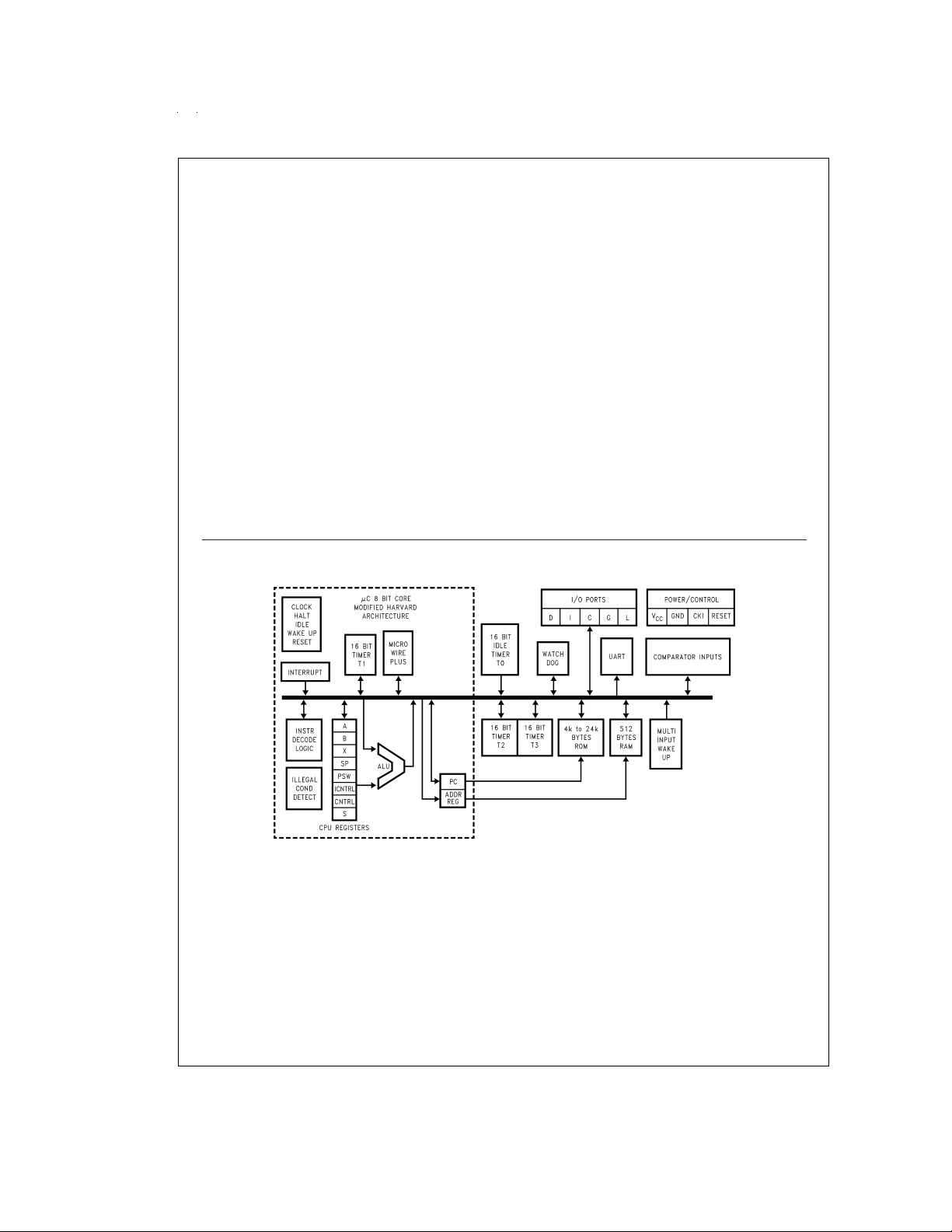
FIGURE 1. COP888xG Block Diagram
www.national.com 2
DS012829-1
Page 3
Connection Diagrams
Top View
Order Number COP884CS-XXX/WM,
COP984CS-XXX/WM,
COP984CSH-XXX/WM, COP684CS-XXX/WM,
COP884CG-XXX/WM,
COP884EG-XXX/WM or
COP884CS-XXX/N, COP984CS-XXX/N,
COP984CSH-XXX/N, COP884CG-XXX/N,
COP884EG-XXX/N
See NS Package Number M28B or N28A
Plastic Chip Carrier
Dual-In-Line Package
DS012829-4
DS012829-3
Top View
Order Number COP888CS-XXX/N, COP988CS-XXX/N,
COP688CS-XXX/N,
COP988CSH-XXX/N, COP888CG-XXX/N,
COP688EG-XXX/N, COP888GG-XXX/N,
COP688GG-XXX/N, COP888GG-XXX/N,
COP688HG-XXX/N, COP888HG-XXX/N,
COP688KG-XXX/N, or COP888KG-XXX/N
See NS Package Number N40A
DS012829-2
Top View
Order Number COP688CS-XXX/V, COP888CS-XXX/V,
COP988CS/CSH-XXX/V, COP688EG-XXX/V,
COP888EG-XXX/V, COP988EG-XXX/V,
COP888CG-XXX/V,
COP688GG-XXX/V, COP888GG-XXX/V,
COP688HG-XXX/V, COP888HG-XXX/V,
COP688KG-XXX/V, or COP888KG-XXX/V
See NS Package Number V44A
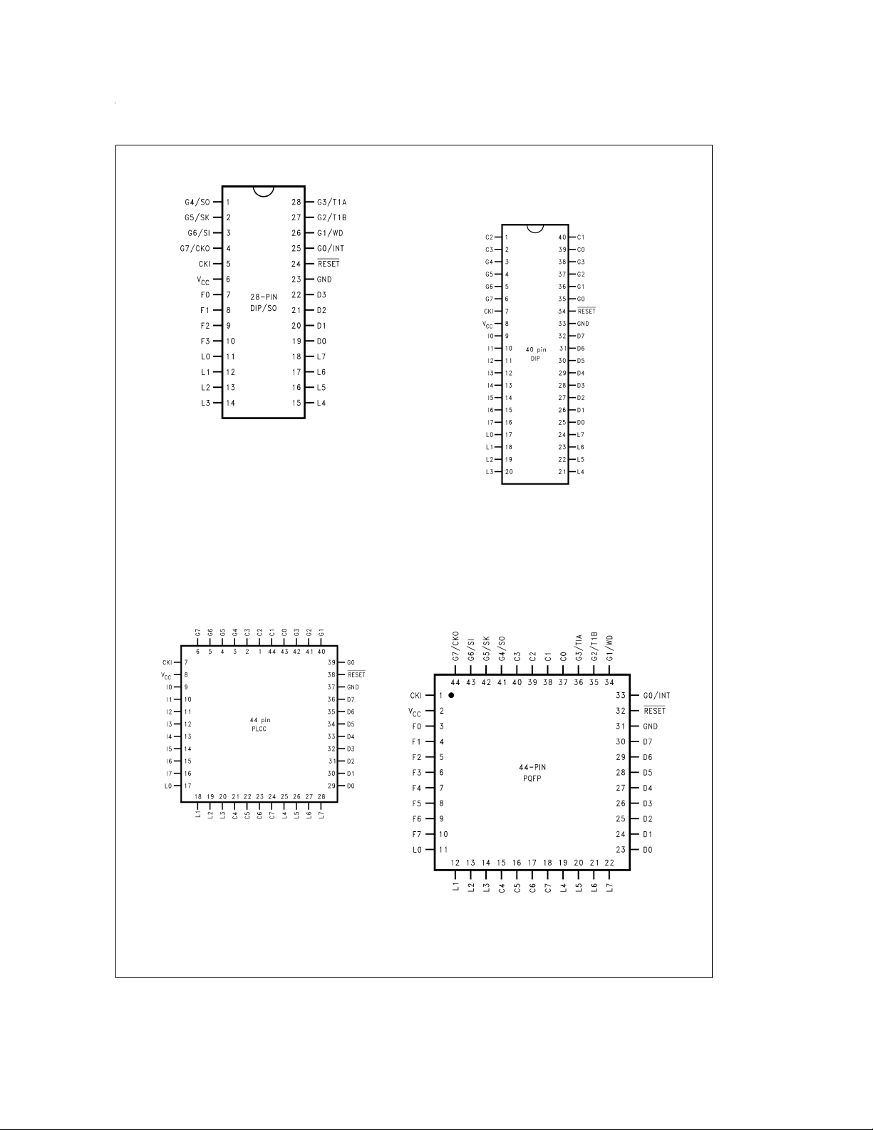
FIGURE 2. Connection Diagrams
DS012829-43
Top View
Order Number COP888EG-XXX/VEJ,
COP688GG-XXX/VEJ, COP888GG-XXX/VEJ,
See NS Package Number VEJ44A
www.national.com3
Page 4

Connection Diagrams (Continued)
Pinouts for 28-, 40- and 44-Pin Packages
Port Type Alt. Fun Alt. Fun
L0 I/O MIWU 11 17 17 11
L1 I/O MIWU CKX 12 18 18 12
L2 I/O MIWU TDX 13 19 19 13
L3 I/O MIWU RDX 14 20 20 14
L4 I/O MIWU T2A* 15 21 25 19
L5 I/O MIWU T2B* 16 22 26 20
L6 I/O MIWU T3A* 17 23 27 21
L7 I/O MIWU T3B* 18 24 28 22
G0 I/O INT 25 35 39 33
G1 WDOUT 26 36 40 34
G2 I/O T1B 27 37 41 35
G3 I/O T1A 28 38 42 36
G4 I/O SO 1 3 3 41
G5 I/O SK 2 4 4 42
G6 I SI 3 5 5 43
G7 I/CKO HALT Restart 4 6 6 44
D0O 19252923
D1O 20263024
D2O 21273125
D3O 22283226
D4 O 29 33 7
D5 O 30 34 8
D6 O 31 35 9
D7O 323610
I0 I 7 9 9 27
I1 I COMP1IN− 8 10 10 28
I2 I COMP1IN+ 9 11 11 29
I3 I COMP1OUT 10 12 12 30
I4 I COMP2IN−* 13 13 3
I5 I COMP2IN+* 14 14 4
I6 I COMP2OUT* 15 15 5
I7 I 16 16 6
C0 I/O 39 43 37
C1 I/O 40 44 38
C2 I/O 1 1 39
C3 I/O 2 2 40
C4 I/O 21 15
C5 I/O 22 16
C6 I/O 23 17
C7 I/O 24 18
V
CC
GND 23 33 37 31
CKI 5 7 7 1
RESET
Note 1:*Not available on the CS series
28-Pin 40-Pin 44-Pin 44-Pin
DIP/SO DIP PLCC PQFP
6882
24 34 38 32
www.national.com 4
Page 5

Absolute Maximum Ratings (Note 4)
If Military/Aerospace specified devices are required,
please contact the National Semiconductor Sales Office/
Distributors for availability and specifications.
Supply Voltage (V
Voltage at Any Pin −0.3V to V
)7V
CC
CC
+ 0.3V
Total Current into V
Pin (Source) 100 mA
CC
Total Current out of GND Pin (Sink) 110 mA
Storage Temperature Range −65˚C to +140˚C
Note 2:
Absolute maximum ratings indicate limits beyond which damage to
the device may occur. DC and AC electrical specifications are not ensured
when operating the device at absolute maximum ratings.
DC Electrical Characteristics 98xEG and 98xCS:
0˚C ≤ TA≤ +70˚C unless otherwise specified
Parameter Conditions Min Typ Max Units
Operating Voltage
COP98xCS, COP98xEG 2.5 4.0 V
COP98xCSH, COP98xEGH 4.0 6.0 V
Power Supply Ripple (Note 6) Peak-to-Peak 0.1 V
Supply Current (Note 7)
CKI=10 MHz V
CKI=4 MHz V
CKI=4 MHz V
CKI=1 MHz V
HALT Current (Note 8) V
=
CC
=
CC
=
CC
=
CC
=
CC
=
V
CC
=
6.0V, t
6.0V, t
4V, t
4V, t
6.0V, CKI=0 MHz
4V, CKI=0 MHz
1 µs 12.5 mA
c
=
2.5 µs 5.5 mA
c
=
2.5 µs 2.5 mA
c
=
10 µs 1.4 mA
c
<
0.7 8 µA
<
0.3 4 µA
IDLE Current
CKI=10 MHz V
CKI=4 MHz V
CKI=1 MHz V
Input Levels (V
IH,VIL
)
=
CC
=
CC
=
CC
=
6.0V, t
6.0V, t
4V, t
1 µs 3.5 mA
c
=
2.5 µs 2.5 mA
c
=
10 µs 0.7 mA
c
RESET
Logic High 0.8 V
CC
Logic Low 0.2 V
CKI (External adn Crystal Osc.
Modes)
Logic High 0.7 V
CC
Logic Low 0.2 V
All Other Inputs
Logic High 0.7 V
CC
Logic Low 0.2 V
Hi-Z Input Leakage V
Input Pullup Current V
=
6.0V, V
CC
=
6.0V, V
CC
=
0V −1 +1 µA
IN
=
0V −40 −250 µA
IN
G and L Port Input Hysteresis (Note 10) 0.35 V
Output Current Levels
D Outputs
Source V
Sink V
=
CC
=
V
CC
=
CC
=
V
CC
4V, V
2.5V, V
4V, V
2.5V, V
=
3.3V −0.4 mA
OH
=
1.8V −0.2 mA
OH
=
1V 10 mA
OL
=
0.4V 2.0 mA
OL
All Others
Source (Weak Pull-Up Mode) V
Source (Push-Pull Mode) V
Sink (Push-Pull Mode) V
=
CC
=
V
CC
=
CC
=
V
CC
=
CC
=
V
CC
4V, V
2.5V, V
4V, V
2.5V, V
4V, V
2.5V, V
=
2.7V −10 −100 µA
OH
=
1.8V −2.5 −33 µA
OH
=
3.3V −0.4 mA
OH
=
1.8V −0.2 mA
OH
=
0.4V 1.6 mA
OL
=
0.4V 0.7 mA
OL
CC
CC
CC
CC
CC
V
V
V
V
V
V
V
V
www.national.com5
Page 6
DC Electrical Characteristics 98xEG and 98xCS: (Continued)
0˚C ≤ TA≤ +70˚C unless otherwise specified
Parameter Conditions Min Typ Max Units
TRI-STATE Leakage V
=
6.0V −1 +1 µA
CC
Allowable Sink/Source
Current per Pin
D Outputs (Sink) 15 mA
All others 3mA
Maximum Input Current
without Latchup (Notes 9, 10) T
RAM Retention Voltage, V
r
= 25˚
A
500 ns Rise and Fall Time (min) 2 V
±
100 mA
Input Capacitance 7pF
Load Capacitance on D2 1000 pF
AC Electrical Characteristics 98xEG and 98xCS:
0˚C ≤ TA≤ +70˚C unless otherwise specified
Parameter Conditions Min Typ Max Units
Instruction Cycle Time (t
Crystal, Resonator 4V ≤ V
R/C Oscillator 4V ≤ V
Inputs
t
SETUP
t
HOLD
Output Propagation Delay R
t
PD1,tPD0
SO, SK 4V ≤ VCC≤ 6.0V 0.7 µs
All Others 4V ≤ V
MICROWIRE Setup Time (t
MICROWIRE Hold Time (t
MICROWIRE Output Propagation Delay (t
Input Pulse Width (Note 11)
Interrupt Input High Time 1 t
Interrupt Input Low Time 1 t
Timer 1, 2, 3 Input High Time 1 t
Timer 1, 2, 3 Input Low Time 1 t
Reset Pulse Width 1 µs
)
c
2.5V ≤ V
2.5V ≤ V
≤ 6.0V 2.5 DC µs
CC
<
4V 1.0 DC µs
CC
≤ 6.0V 7.5 DC µs
CC
<
4V 3.0 DC µs
CC
4V ≤ VCC≤ 6.0V 200 ns
2.5V ≤ V
<
4V 500 ns
CC
4V ≤ VCC≤ 6.0V 60 ns
2.5V ≤ V
L
2.5V ≤ V
2.5V ≤ V
) (Note 10) 20 ns
UWS
) (Note 10) 56 ns
UWH
) 220 ns
UPD
<
4V 150 ns
CC
=
=
2.2k, C
CC
100 pF
L
<
4V 1.75 µs
CC
≤ 6.0V 1 µs
<
4V 2.5 µs
CC
c
c
c
c
www.national.com 6
Page 7

Absolute Maximum Ratings (Note 4)
If Military/Aerospace specified devices are required,
please contact the National Semiconductor Sales Office/
Distributors for availability and specifications.
Supply Voltage (V
Voltage at Any Pin −0.3V to V
)7V
CC
CC
+ 0.3V
Total Current into V
Pin (Source) 100 mA
CC
Total Current out of GND Pin (Sink) 110 mA
Storage Temperature Range −65˚C to +140˚C
Note 3:
Absolute maximum ratings indicate limits beyond which damage to
the device may occur. DC and AC electrical specifications are not ensured
when operating the device at absolute maximum ratings.
DC Electrical Characteristics 88xCG, 88xCS, and 88xEG:
−40˚C ≤ TA≤ +85˚C unless otherwise specified
Parameter Conditions Min Typ Max Units
Operating Voltage
Power Supply Ripple (Note 6) Peak-to-Peak 0.1 V
Supply Current (Note 7)
CKI=10 MHz V
CKI=4 MHz V
CKI=4 MHz
(88xCG & 88xEG only)
CKI=1 MHz
(88xCG & 88xEG only)
HALT Current (Note 8) V
(88xCG & 88xEG only) V
=
CC
=
CC
=
V
CC
=
V
CC
=
CC
=
CC
IDLE Current
CKI=10 MHz V
CKI=4 MHz V
CKI=1 MHz
(88xCG & 88xEG only)
Input Levels (V
IH,VIL
)
=
CC
=
CC
=
V
CC
RESET
Logic High 0.8 V
Logic Low 0.2 V
CKI (External adn Crystal Osc.
Modes)
Logic High 0.7 V
Logic Low 0.2 V
All Other Inputs
Logic High 0.7 V
Logic Low 0.2 V
Hi-Z Input Leakage V
Input Pullup Current V
=
CC
=
CC
G and L Port Input Hysteresis (Note 10) 0.35 V
Output Current Levels
D Outputs
Source V
Sink V
=
CC
=
V
CC
=
CC
=
V
CC
All Others
Source (Weak Pull-Up Mode) V
Source (Push-Pull Mode) V
Sink (Push-Pull Mode) V
=
CC
=
V
CC
=
CC
=
V
CC
=
CC
=
6.0V, t
6.0V, t
4V, t
4V, t
6.0V, CKI=0 MHz
4V, CKI=0 MHz
6.0V, t
6.0V, t
4V, t
1 µs 12.5 mA
c
=
2.5 µs 5.5 mA
c
=
2.5 µs 2.5 mA
c
=
10 µs 1.4 mA
c
<
1.0 8 µA
<
0.5 4 µA
=
1 µs 3.5 mA
c
=
2.5 µs 2.5 mA
c
=
10 µs 0.7 mA
c
CC
CC
CC
6.0V −2 +2 µA
6.0V, V
4V, V
2.5V, V
4V, V
2.5V, V
4V, V
2.5V, V
4V, V
2.5V, V
4V, V
=
0V −40 −250 µA
IN
=
3.3V −0.4 mA
OH
=
1.8V −0.2 mA
OH
=
1V 10 mA
OL
=
0.4V 2.0 mA
OL
=
2.7V −10 −100 µA
OH
=
1.8V −2.5 −33 µA
OH
=
3.3V −0.4 mA
OH
=
1.8V −0.2 mA
OH
=
0.4V 1.6 mA
OL
CC
V
V
CC
V
V
CC
V
V
CC
CC
V
V
www.national.com7
Page 8
DC Electrical Characteristics 88xCG, 88xCS, and 88xEG: (Continued)
−40˚C ≤ TA≤ +85˚C unless otherwise specified
Parameter Conditions Min Typ Max Units
TRI-STATE Leakage V
=
V
2.5V, V
CC
=
6.0V −1 +1 µA
CC
=
0.4V 0.7 mA
OL
Allowable Sink/Source
Current per Pin
D Outputs (Sink) 15 mA
All others 3mA
Maximum Input Current
without Latchup (Notes 9, 10) T
RAM Retention Voltage, V
r
= 25˚
A
500 ns Rise and Fall Time (min) 2 V
±
100 mA
Input Capacitance 7pF
Load Capacitance on D2 1000 pF
AC Electrical Characteristics 888EG, 88xCS, and 88xCG:
−40˚C ≤ TA≤ +85˚C unless otherwise specified
Parameter Conditions Min Typ Max Units
Instruction Cycle Time (t
Crystal, Resonator 4V ≤ V
R/C Oscillator 4V ≤ V
Inputs
t
SETUP
t
HOLD
Output Propagation Delay R
t
PD1,tPD0
SO, SK 4V ≤ VCC≤ 6.0V 0.7 µs
All Others 4V ≤ V
MICROWIRE Setup Time (t
MICROWIRE Hold Time (t
MICROWIRE Output Propagation Delay (t
Input Pulse Width (Note 11)
Interrupt Input High Time 1 t
Interrupt Input Low Time 1 t
Timer 1, 2, 3 Input High Time 1 t
Timer 1, 2, 3 Input Low Time 1 t
Reset Pulse Width 1 µs
)
c
2.5V ≤ V
2.5V ≤ V
≤ 6.0V 1.0 DC µs
CC
<
4V 2.5 DC µs
CC
≤ 6.0V 3.0 DC µs
CC
<
4V 7.5 DC µs
CC
4V ≤ VCC≤ 6.0V 200 ns
2.5V ≤ V
<
4V 500 ns
CC
4V ≤ VCC≤ 6.0V 60 ns
2.5V ≤ V
L
2.5V ≤ V
2.5V ≤ V
) (Note 10) 20 ns
UWS
) (Note 10) 56 ns
UWH
) 220 ns
UPD
<
4V 150 ns
CC
=
=
2.2k, C
CC
100 pF
L
<
4V 1.75 µs
CC
≤ 6.0V 1 µs
<
4V 2.5 µs
CC
c
c
c
c
www.national.com 8
Page 9

Absolute Maximum Ratings (Note 4)
If Military/Aerospace specified devices are required,
please contact the National Semiconductor Sales Office/
Distributors for availability and specifications.
Supply Voltage (V
Voltage at Any Pin −0.3V to V
)7V
CC
CC
+ 0.3V
Total Current into V
Pin (Source) 100 mA
CC
Total Current out of GND Pin (Sink) 110 mA
Storage Temperature Range −65˚C to +140˚C
Note 4:
Absolute maximum ratings indicate limits beyond which damage to
the device may occur. DC and AC electrical specifications are not ensured
when operating the device at absolute maximum ratings.
DC Electrical Characteristics 888GG, 888HG, and 888KG:
−40˚C ≤ TA≤ +85˚C unless otherwise specified
Parameter Conditions Min Typ Max Units
Operating Voltage 2.5 5.5 V
Power Supply Ripple (Note 6) Peak-to-Peak 0.1 V
CC
Supply Current (Note 7)
CKI=10 MHz V
CKI=4 MHz V
CKI=4 MHz V
CKI=1 MHz V
HALT Current (Note 8) V
=
CC
=
CC
=
CC
=
CC
=
CC
=
V
CC
=
5.5V, t
5.5V, t
4V, t
4V, t
5.5V, CKI=0 MHz
4V, CKI=0 MHz
1 µs 12.5 mA
c
=
2.5 µs 5.5 mA
c
=
2.5 µs 2.5 mA
c
=
10 µs 1.4 mA
c
<
110 µA
<
0.5 6 µA
IDLE Current
CKI=10 MHz V
CKI=4 MHz V
CKI=1 MHz V
Input Levels (V
IH,VIL
)
=
CC
=
CC
=
CC
=
5.5V, t
5.5V, t
4V, t
1 µs 3.5 mA
c
=
2.5 µs 2.5 mA
c
=
10 µs 0.7 mA
c
RESET
Logic High 0.8 V
Logic Low 0.2 V
CC
CC
CKI, All Other Inputs
Logic High 0.7 V
Logic Low 0.2 V
Hi-Z Input Leakage V
Input Pullup Current V
=
5.5V, V
CC
=
5.5V, V
CC
=
0V −2 +2 µA
IN
=
0V −40 −250 µA
IN
G and L Port Input Hysteresis (Note 10) 0.35 V
CC
CC
CC
Output Current Levels
D Outputs
Source V
Sink V
=
CC
=
V
CC
=
CC
=
V
CC
4V, V
2.5V, V
4V, V
2.5V, V
=
3.3V −0.4 mA
OH
=
1.8V −0.2 mA
OH
=
1V 10 mA
OL
=
0.4V 2.0 mA
OL
All Others
Source (Weak Pull-Up Mode) V
Source (Push-Pull Mode) V
Sink (Push-Pull Mode) V
TRI-STATE Leakage V
=
CC
=
V
CC
=
CC
=
V
CC
=
CC
=
V
CC
=
CC
=
4V, V
2.5V, V
4V, V
2.5V, V
4V, V
2.5V, V
2.7V −10 −100 µA
OH
=
1.8V −2.5 −33 µA
OH
=
3.3V −0.4 mA
OH
=
1.8V −0.2 mA
OH
=
0.4V 1.6 mA
OL
=
0.4V 0.7 mA
OL
5.5V −2 +2 µA
Allowable Sink/Source
Current per Pin
D Outputs (Sink) 15 mA
All others 3mA
Maximum Input Current
V
V
V
V
V
V
www.national.com9
Page 10
DC Electrical Characteristics 888GG, 888HG, and 888KG: (Continued)
−40˚C ≤ TA≤ +85˚C unless otherwise specified
Parameter Conditions Min Typ Max Units
±
without Latchup (Notes 9, 10) Room Temperature
RAM Retention Voltage, V
r
500 ns Rise and Fall Time (min) 2 V
100 mA
Input Capacitance 7pF
Load Capacitance on D2 (Note 10) 1000 pF
AC Electrical Characteristics 888GG, 888HG, and 888KG:
−40˚C ≤ TA≤ +85˚C unless otherwise specified
Parameter
(88xCG & 88xEG only)
Instruction Cycle Time (t
)
c
Crystal, Resonator 2.5V ≤ V
R/C Oscillator 2.5V ≤ V
Inputs
t
SETUP
t
HOLD
Output Propagation Delay R
t
PD1,tPD0
SO, SK 4V ≤ VCC≤ 5.5V 0.7 µs
All Others 4V ≤ V
MICROWIRE Setup Time (t
MICROWIRE Hold Time (t
MICROWIRE Output Propagation Delay (t
) (Note 10) VCC≥ 4V 20 ns
UWS
) (Note 10) VCC≥ 4V 56 ns
UWH
)VCC≥ 4V 220 ns
UPD
Input Pulse Width (Note 11)
Interrupt Input High Time 1 t
Interrupt Input Low Time 1 t
Timer 1, 2, 3 Input High Time 1 t
Timer 1, 2, 3 Input Low Time 1 t
Reset Pulse Width 1 µs
Conditions Min Typ Max Units
<
4V 1.0 DC µs
CC
4V ≤ V
4V ≤ V
≤ 5.5V 2.5 DC µs
CC
<
4V 3.0 DC µs
CC
≤ 5.5V 7.5 DC µs
CC
4V ≤ VCC≤ 5.5V 200 ns
2.5V ≤ V
<
4V 500 ns
CC
4V ≤ VCC≤ 5.5V 60 ns
2.5V ≤ V
L
2.5V ≤ V
2.5V ≤ V
<
4V 150 ns
CC
=
=
2.2k, C
CC
100 pF
L
<
4V 1.75 µs
CC
≤ 5.5V 1 µs
<
4V 2.5 µs
CC
c
c
c
c
www.national.com 10
Page 11
Absolute Maximum Ratings (Note 5)
If Military/Aerospace specified devices are required,
please contact the National Semiconductor Sales Office/
Distributors for availability and specifications.
Supply Voltage (V
Voltage at Any Pin −0.3V to V
)7V
CC
CC
+ 0.3V
Total Current into V
Pin (Source) 100 mA
CC
Total Current out of GND Pin (Sink) 110 mA
Storage Temperature Range −65˚C to +140˚C
Note 5:
Absolute maximum ratings indicate limits beyond which damage to
the device may occur. DC and AC electrical specifications are not ensured
when operating the device at absolute maximum ratings.
DC Electrical Characteristics 68xCS and 68xxG:
−55˚C ≤ TA≤ +125˚C unless otherwise specified
Parameter Conditions Min Typ Max Units
Operating Voltage 4.5 5.5 V
Power Supply Ripple (Note 6) Peak-to-Peak 0.1 V
Supply Current (Note 7)
CKI=10 MHz V
CKI=4 MHz V
HALT Current (Note 8) V
=
CC
=
CC
=
CC
=
5.5V, t
5.5V, t
1 µs 12.5 mA
c
=
2.5 µs 5.5 mA
c
5.5V, CKI=0 MHz
<
10 30 µA
IDLE Current
CKI=10 MHz V
CKI=4 MHz V
Input Levels (V
IH,VIL
)
=
CC
=
CC
5.5V, t
5.5V, t
=
1 µs 3.5 mA
c
=
2.5 µs 2.5 mA
c
RESET
Logic High 0.8 V
CC
Logic Low 0.2 V
CKI (68xCS & 68xEG only)
Logic High 0.7 V
CC
Logic Low 0.2 V
All Other Inputs
Logic High 0.7 V
CC
Logic Low 0.2 V
Hi-Z Input Leakage V
Input Pullup Current V
=
5.5V, V
CC
=
5.5V, V
CC
=
0V −5 +5 µA
IN
=
0V −35 −400 µA
IN
G and L Port Input Hysteresis (Note 10) 0.35 V
Output Current Levels
D Outputs
Source V
Sink V
=
4.5V, V
CC
=
4.5V, V
CC
=
3.3V −0.4 mA
OH
=
1V 9 mA
OL
All Others
Source (Weak Pull-Up Mode) V
Source (Push-Pull Mode) V
Sink (Push-Pull Mode) V
TRI-STATE Leakage V
=
4.5V, V
CC
=
4.5V, V
CC
=
4.5V, V
CC
=
5.5V −5 +5 µA
CC
=
2.7V −9 −140 µA
OH
=
3.3V −0.4 mA
OH
=
0.4V 1.4 mA
OL
Allowable Sink/Source
Current per Pin
D Outputs (Sink) 12 mA
All others 2.5 mA
Maximum Input Current
without Latchup (Notes 9, 10) Room Temp
RAM Retention Voltage, V
r
500 ns Rise and Fall Time (min) 2 V
Input Capacitance (Note 10) 7 pF
Load Capacitance on D2 (Note 10) 1000 pF
CC
CC
CC
CC
CC
±
100 mA
V
V
V
V
V
V
V
V
www.national.com11
Page 12
AC Electrical Characteristics 68xCS and 68xxG:
−55˚C ≤ TA≤ +125˚C unless otherwise specified
Parameter Conditions Min Typ Max Units
Instruction Cycle Time (t
Crystal, Resonator V
R/C Oscillator
68xCS & 68xEG only)
Inputs
t
SETUP
t
HOLD
Output Propagation Delay R
t
PD1,tPD0
SO, SK VCC≥ 4.5V 0.7 µs
All Others V
MICROWIRE
™
MICROWIRE Hold Time (t
MICROWIRE Output Propagation Delay (t
Input Pulse Width (Note 11)
Interrupt Input High Time 1 t
Interrupt Input Low Time 1 t
Timer 1, 2, 3 Input High Time 1 t
Timer 1, 2, 3 Input Low Time 1 t
Reset Pulse Width 1 µs
Note 6: Maximum rate of voltage change must be less than 0.5 V/ms.
Note 7: Supply current is measured after running 2000 cycles with a square wave CKI input, CKO open, inputs at rails and outputs open.
Note 8: The HALT mode will stop CKI from oscillating in the RC and the Crystal configurations. Measurement of IDD HALTis done with device neither sourcing or
sinking current; with L, C, and G0–G5 programmed as low outputs and not driving a load; all outputs programmed low and not driving a load; all inputs tied to V
clock monitor and comparatorsdisabled. Parameter refers toHALTmode entered via setting bit 7 of theG Port data register.Partwill pull up CKIduring HALTin crystal clock mode.
Note 9: Pins G6 and RESET are designed with a high voltage input network. These pins allow input voltages greater than V
to VCCwhen biased atvoltages greater thanVCC(the pins donot have sourcecurrent when biasedat a voltagebelow VCC). The effective resistance to VCCis 750Ω
(typical). These two pins will not latch up. The voltage at the pins must be limited to less than 14V. WARNING: Voltagesin excess of 14V will cause damage to the
pins. This warning excludes ESD transients.
Note 10: Parameter characterized but not tested.
Note 11: t
=
Instruction Cycle Time
c
)
c
Setup Time (t
UWH
≥ 4.5V 1.0 DC µs
CC
V
≥ 4.5V 3.0 DC µs
CC
VCC≥ 4.5V 200 ns
VCC≥ 4.5V 60 ns
=
L
≥ 4.5V 1 µs
) (Note 10) 20 ns
UWS
CC
2.2k, C
L
=
100 pF
) (Note 10) 56 ns
) 220 ns
UPD
and the pins will have sink current
CC
c
c
c
c
;
CC
Comparators AC and DC Characteristics
=
V
5V, −40˚C ≤ T
CC
Input Offset Voltage 0.4V ≤ V
Input Common Mode Voltage Range 0.4 V
Voltage Gain 300k V/V
Low Level Output Current V
High Level Output Current V
DC Supply Current per Comparator (When Enabled) 250 µA
Response Time 100 mV Overdrive, 1 µs
www.national.com 12
≤ +85˚C.
A
Parameter Conditions Min Typ Max Units
≤ VCC− 1.5V
IN
=
0.4V 1.6 mA
OL
=
4.6V 1.6 mA
OH
±
10
±
25 mV
− 1.5 V
CC
100 pF Load
Page 13
Comparators AC and DC Characteristics (Continued)
DS012829-4
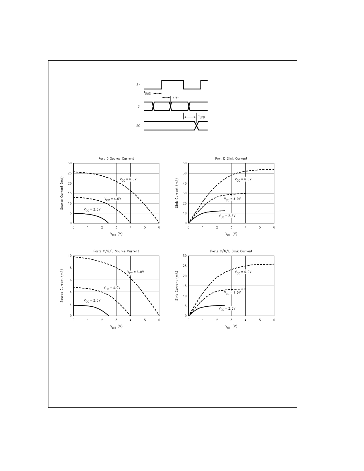
FIGURE 3. MICROWIRE/PLUS Timing
Typical Performance Characteristics (−55˚C ≤ T
DS012829-30 DS012829-31
A
=
+125˚C)
DS012829-32 DS012829-33
www.national.com13
Page 14
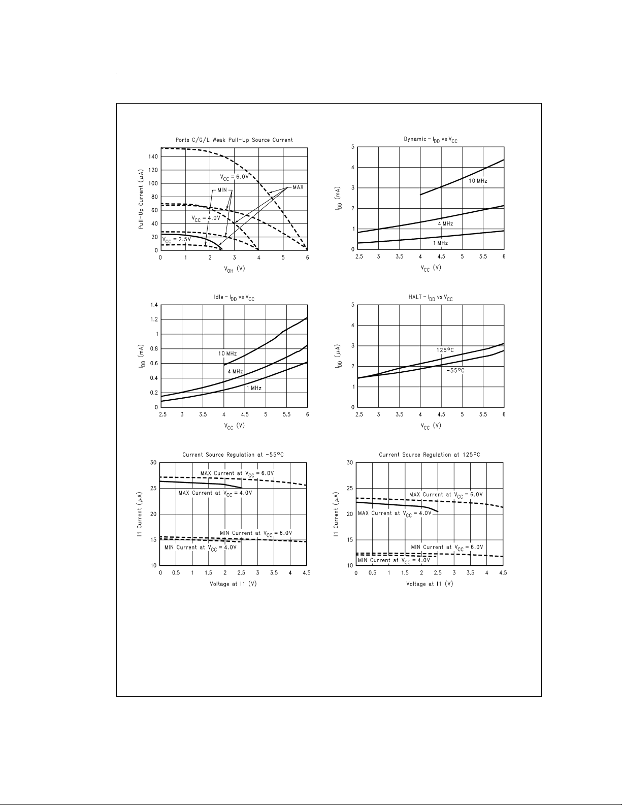
Typical Performance Characteristics (−55˚C ≤ T
=
+125˚C) (Continued)
A
DS012829-34
DS012829-36 DS012829-37
DS012829-35
DS012829-38 DS012829-39
www.national.com 14
Page 15
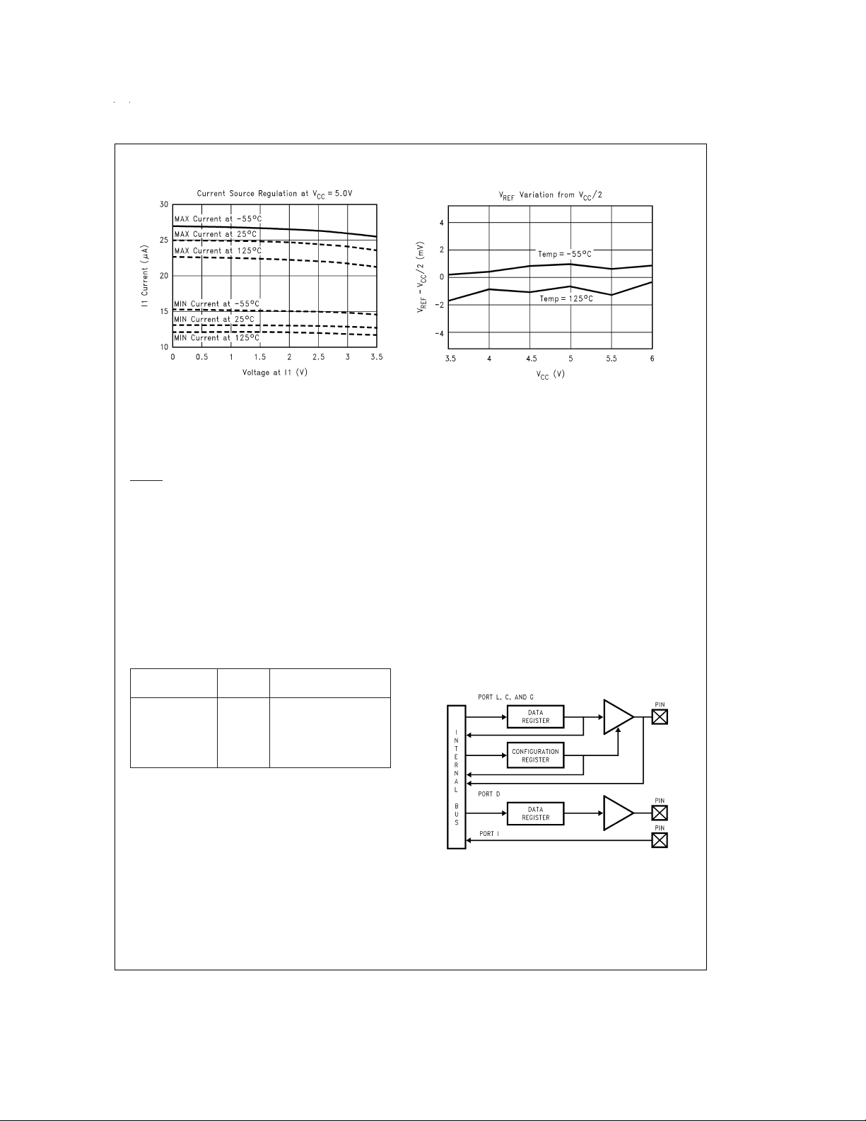
Typical Performance Characteristics (−55˚C ≤ T
=
+125˚C) (Continued)
A
DS012829-40
Pin Descriptions
VCCand GND are the power supply pins. All VCCand GND
pins must be connected.
CKI isthe clock input. This can come from an R/C generated
oscillator, or a crystal oscillator (in conjunction with CKO).
See Oscillator Description section.
RESET is the master reset input.See ResetDescription section.
The device contains three bidirectional 8-bit I/O ports (C, G
and L), where each individual bit may be independently configured asan input (SchmittTrigger inputs on ports L and G),
output or TRI-STATE under program control. Three data
memory address locations are allocated for each of these
I/O ports. Each I/O port has two associated 8-bit memory
mapped registers, the CONFIGURATION register and the
output DATAregister. A memory mapped address is also reserved for the input pins of each I/O port. (See the memory
map for the various addresses associatedwith theI/O ports.)
Figure 4
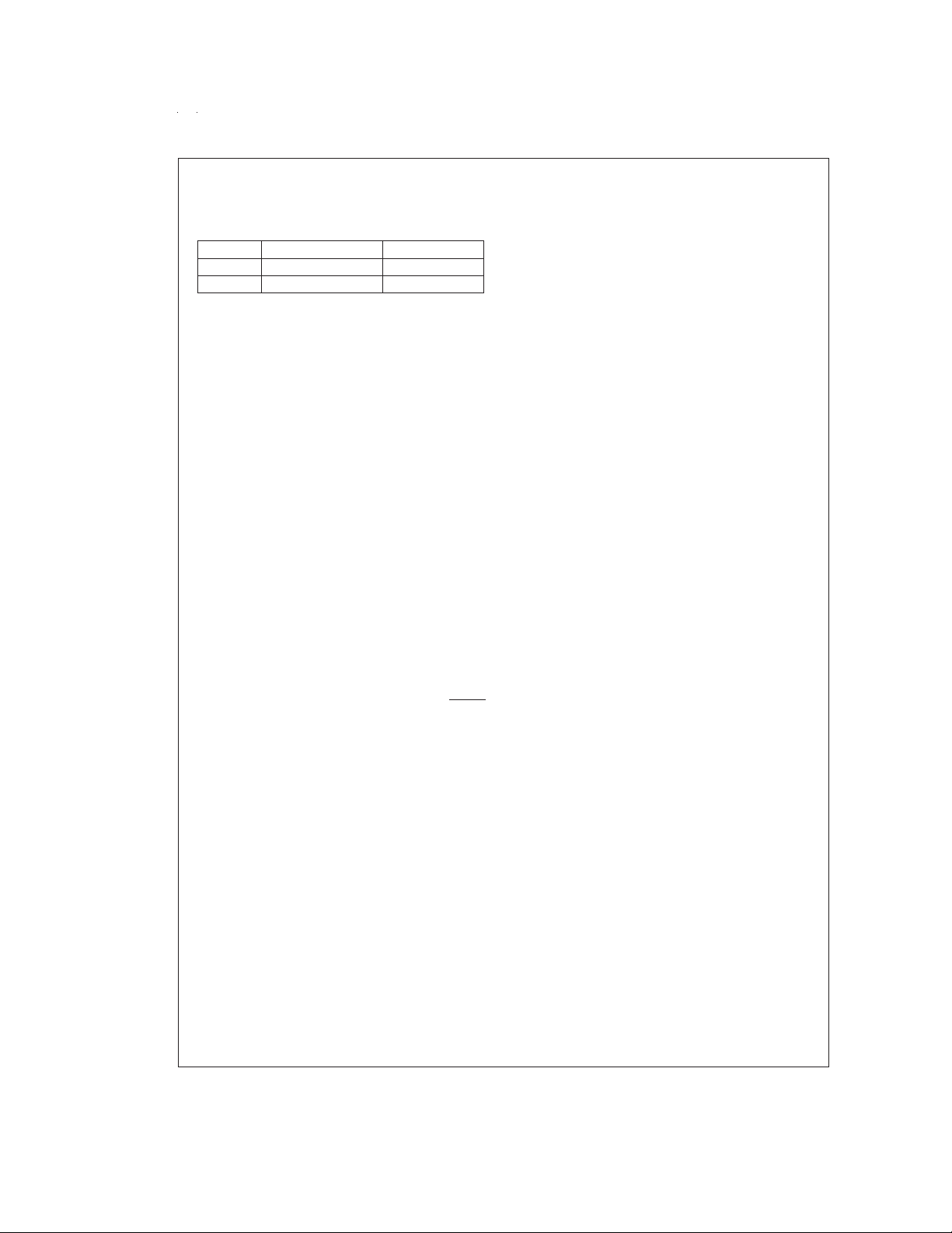
shows the I/O port configurations. The DATA and
CONFIGURATION registers allow for each port bit to be individually configured under software control as shown below:
CONFIGURATION DATA Port Set-Up
Register Register
0 0 Hi-Z Input
0 1 Input with Weak Pull-Up
1 0 Push-Pull Zero Output
1 1 Push-Pull One Output
PORT L is an 8-bit I/O port. All L-pins have Schmitt triggers
on the inputs.
The Port L supports Multi-Input WakeUp on all eight pins. L1
is used for the USART external clock. L2 andL3 are used for
the USARTtransmit and receive. L4 and L5 are used for the
timer input functions T2A and T2B. L6 and L7 are used for
the timer input functions T3Aand T3B (execpt on the CS series).
The Port L has the following alternate features:
L7 MIWU or T3B
L6 MIWU or T3A
L5 MIWU or T2B
L4 MIWU or T2A
L3 MIWU or RDX
(TRI-STATE Output)
DS012829-41
L2 MIWU or TDX
L1 MIWU or CKX
L0 MIWU
Port G is an 8-bit port with 5 I/O pins (G0, G2–G5), an input
pin (G6), and a dedicated output pin (G1). Pins G0 and
G2–G6 all have Schmitt Triggers on their inputs. Pin G1
serves as the dedicated WDOUT WATCHDOG output, while
pin G7 is either input or output depending on the oscillator
mask option selected. With the crystal oscillator option selected, G7 serves as the dedicated output pin for the CKO
clock output. With the single-pin R/C oscillator mask option
selected, G7 serves as a general purpose input pin but is
also used to bring the device out of HALT mode with a low to
high transition on G7. There are two registers associated
with the G Port, a data register and a configuration register.
Therefore, each of the 5 I/O bits (G0, G2–G5) can be individually configured under software control.
Since G6 is an input only pin and G7 is the dedicated CKO
clock output pin (crystal clock option) or general purpose input (R/C clock option), the associated bits in the data and
configuration registers for G6 and G7 are used for special
purpose functions as outlined on the next page. Reading the
G6 and G7 data bits will return zeros.
DS012829-5
FIGURE 4. I/O Port Configurations
Note thatthe chip will be placed in the HALT mode by writing
a “1” to bit 7 of the Port G Data Register. Similarly the chip
will beplaced in theIDLE mode by writing a “1” to bit 6 of the
Port G Data Register.
Writing a “1” to bit 6 of the Port G Configuration Register enables the MICROWIRE/PLUS to operate with the alternate
www.national.com15
Page 16
Pin Descriptions (Continued)
phase of the SK clock. The G7 configuration bit, if set high,
enables the clock start up delay after HALT when the R/C
clock configuration is used.
Config Reg. Data Reg.
G7 CLKDLY HALT
G6 Alternate SK IDLE
Port G has the following alternate features:
G6 SI (MICROWIRE Serial Data Input)
G5 SK (MICROWIRE Serial Clock)
G4 SO (MICROWIRE Serial Data Output)
G3 T1A (Timer T1 I/O)
G2 T1B (Timer T1 Capture Input)
G0 INTR (External Interrupt Input)
Port G has the following dedicated functions:
G7 CKO Oscillator dedicated output or general purpose
input
G1 WDOUT WATCHDOG and/or Clock Monitor dedi-
cated output
Port C is an 8-bit I/O port. The 40-pin device does not have
a full complement of Port C pins. The unavailable pins are
not terminated.A read operation for these unterminated pins
will return unpredicatable values.
Port I is an eight-bit Hi-Z input port.
Port I1–I3 are used forComparator 1.Port I4–I6 are used for
Comparator 2.
The Port I has the following alternate features:
I6 COMP2OUT (Comparator 2 Output)
I5 COMP2+IN (Comparator 2 Positive Input)
I4 COMP2−IN (Comparator 2 Negative Input)
I3 COMP1OUT (Comparator 1 Output)
I2 COMP1+IN (Comparator 1 Positive Input)
I1 COMP1−IN (Comparator 1 Negative Input)
Port D is an 8-bit output port that ispreset high when RESET
goes low. The user can tie two or more D port outputs (except D2) together in order to get a higher drive.
Functional Description
The architecture of the device is modified Harvard architecture. With the Harvard architecture, the control store program memory (ROM) is separated from the data store
memory (RAM). Both ROM and RAM have their own separate addressing space with separate address buses.The architecture, though based on Harvard architecture, permits
transfer of data from ROM to RAM.
CPU REGISTERS
The CPU can doan 8-bit addition, subtraction, logicalor shift
operation in one instruction (t
There are six CPU registers:
A is the 8-bit Accumulator Register
PC is the 15-bit Program Counter Register
PU is the upper 7 bits of the program counter (PC)
PL is the lower 8 bits of the program counter (PC)
B is an 8-bit RAM address pointer, which can be optionally
post auto incremented or decremented.
X is an 8-bit alternate RAM address pointer, which can be
optionally post auto incremented or decremented.
www.national.com 16
) cycle time.
c
SP is the 8-bit stack pointer, which points to the subroutine/
interrupt stack (in RAM). The SP is initialized to RAM address 06F with reset.
S is the 8-bitData SegmentAddress Register used to extend
the lower half of the address range (00 to 7F) into 256 data
segments of 128 bytes each.
All the CPU registers are memory mapped with the exception of the Accumulator (A) and the Program Counter (PC).
PROGRAM MEMORY
The program memory consists of up to 24 kbytes of ROM.
These bytes may hold program instructions or constant data
(data tablesfor the LAIDinstruction, jump vectors for the JID
instruction, and interrupt vectors for the VIS instruction). The
program memory is addressed by the 15-bit program
counter (PC). All interrupts in the devices vector to program
memory location 0FF Hex.
DATA MEMORY
The data memory address space includes the on-chip RAM
and data registers, theI/O registers (Configuration, Data and
Pin), the control registers, the MICROWIRE/PLUS SIO shift
register, and the various registers, and counters associated
with the timers (with the exception of the IDLE timer). Data
memory is addressed directly by the instruction or indirectly
by the B, X, SP pointers and S register.
The data memory consists of up to 512 bytes of RAM. Sixteen bytes of RAM are mapped as “registers” at addresses
0F0 to0FF Hex. These registers can be loaded immediately,
and also decremented and tested withthe DRSZ(decrement
register and skip if zero) instruction. The memory pointer
registers X,SP,B and S are memorymapped into thisspace
at address locations 0FC to 0FF Hex respectively, with the
other registers being available for general usage.
The instructionset permits anybit in memoryto be set,reset
or tested. All I/O and registers (except A and PC) are
memory mapped; therefore, I/O bits and register bits can be
directly andindividually set, reset and tested. The accumulator (A) bits can also be directly and individually tested.
Note: RAM contents are undefined upon power-up.
Data Memory Segment RAM
Extension
Data memory address 0FF is used as a memory mapped location for the Data Segment Address Register (S).
The data store memory is either addressed directly by a
single byte address within the instruction, or indirectly relative to the reference of the B, X, or SP pointers (each contains a single-byte address). This single-byte address allows
an addressingrange of 256 locations from 00 to FF hex. The
upper bit of this single-byte address divides the data store
memory into two separate sections as outlined previously.
With the exception of the RAM register memory from address locations 00F0 to 00FF, all RAM memory is memory
mapped with the upper bit of the single-byte address being
equal to zero. This allows the upper bit of the single-byte address to determine whether or not the base address range
(from 0000 to 00FF) is extended. If this upper bit equals one
(representing address range 0080 to 00FF), then address
extension does not take place. Alternatively, if this upper bit
equals zero, then the data segment extension register S is
used to extend the base address range (from 0000 to 007F)
from XX00 to XX7F,where XX represents the 8 bits from the
S register. Thus the 128-byte data segment extensions are
located from addresses 0100 to 017F for data segment 1,
Page 17
Data Memory Segment RAM
Extension
0200 to 027F for data segment 2, etc., up to FF00 to FF7F
for data segment 255. The base address range from 0000 to
007F represents data segment 0.
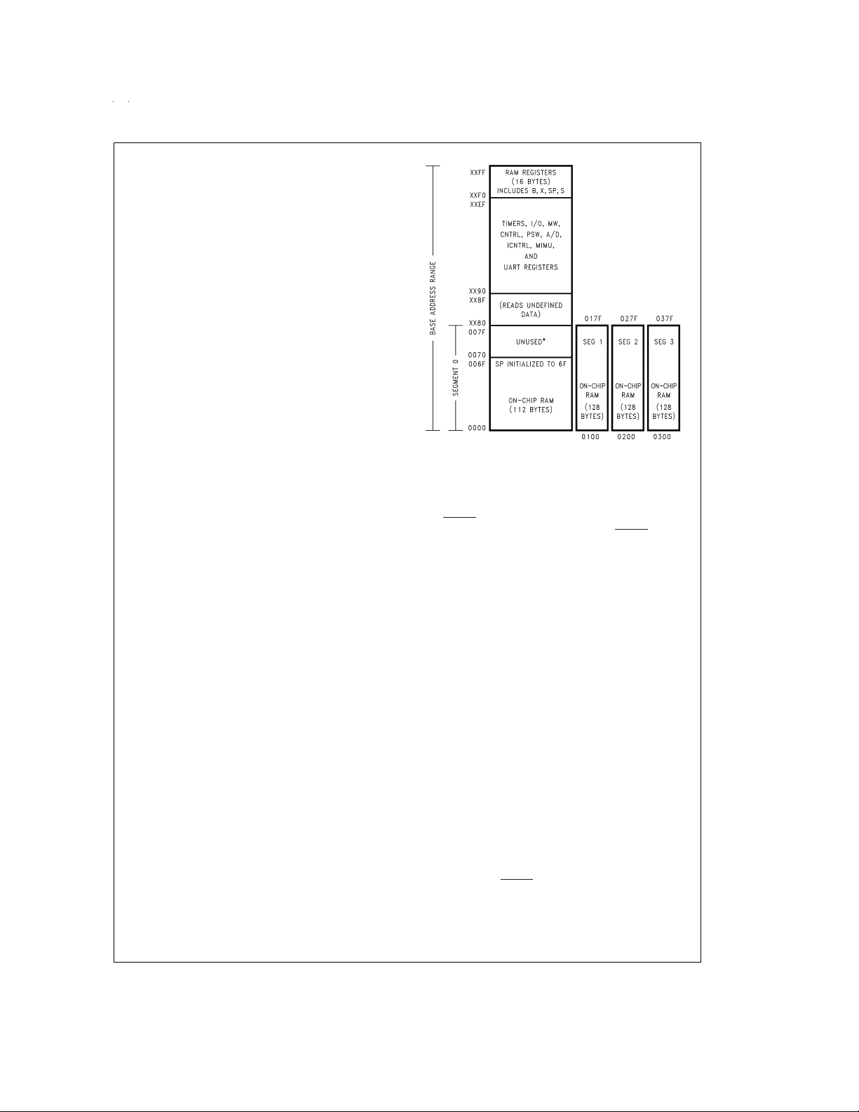
Figure 5
sion is used in extending the lower half of the base address
range (00 to 7F hex) into 256 data segments of 128 bytes
each, with a total addressing range of 32 kbytes from XX00
to XX7F. This organization allows a total of 256 data segments of 128 bytes each with an additional upper base segment of 128 bytes. Furthermore, all addressing modes are
available for all data segments. The S register must be
changed under program control to move from one data segment (128 bytes) to another. However, the upper base segment (containing the 16 memory registers, I/O registers,
control registers, etc.) is always available regardless of the
contents of the S register, since the upper base segment
(address range 0080 to 00FF) is independent of data segment extension.
The instructions that utilize the stack pointer(SP) always reference the stack as part of the base segment (Segment 0),
regardless of the contents of the S register. The S register is
not changed by these instructions. Consequently, the stack
(used with subroutine linkage and interrupts) is always located in the base segment. The stack pointer will be intitialized to point at data memory location 006F as a result of reset.
The 128 bytes of RAM contained in the base segment are
split between the lower and upper base segments. The first
112bytes of RAM are resident from address 0000 to006F in
the lower base segment, while the remaining 16 bytes of
RAM represent the 16 data memory registers located at addresses 00F0 to 00FF of the upper base segment. No RAM
is located at the upper sixteen addresses (0070 to 007F) of
the lower base segment.
Additional RAM beyond these initial 128 bytes, however, will
always be memory mapped in groups of 128 bytes (or less)
at the data segment address extensions (XX00 to XX7F) of
the lower base segment. The additional bytes of RAM are
memory mapped from segment 1 upthrough segment3 (see
Figure 5
).
(Continued)
illustrates how the S register data memory exten-
*
Reads as all ones.
FIGURE 5. RAM Organization
DS012829-6
Reset
The RESET input when pulled low initializes the microcontroller. Initialization will occur whenever the RESET input is
pulled low. Upon initialization, the data and configuration
registers for ports L, G and C are cleared, resulting in these
Ports being initialized to the TRI-STATEmode. Pin G1 of the
G Portis an exception (as noted below) since pin G1 is dedicated as the WATCHDOG and/or Clock Monitor error output
pin. Port D is set high. The PC, PSW, ICNTRL, CNTRL,
T2CNTRL and T3CNTRL control registers are cleared. The
USART registers PSR, ENU (except that TBMT bit is set),
ENUR andENUI are cleared. The Comparator Select Register is cleared. The S register is initialized to zero. The
Multi-Input Wakeup registers WKEN and WKEDG are
cleared. Wakeup register WKPND is unknown. The stack
pointer, SP, is initialized to 6F hex.
The device comes out of reset with both the WATCHDOG
logic and the Clock Monitor detector armed, with the
WATCHDOG service window bits set and the Clock Monitor
bit set. The WATCHDOG and Clock Monitor circuits are inhibited during reset. The WATCHDOG service window bits
being initialized high default to the maximum WATCHDOG
service window of 64k t
being initialized high will cause a Clock Monitor error following reset if the clock has not reached the minimum specified
frequency at the termination of reset. A Clock Monitor error
will cause an active low error output on pin G1. This error
output will continue until 16 t
the clock frequency reaching the minimum specified value,
at which time the G1 output will enter the TRI-STATE mode.
The external RC network shown in
to ensure that the RESET pin is held lowuntil the power supply to the chip stabilizes.
clock cycles. The Clock Monitor bit
C
–32 tCclock cycles following
C
Figure 6
should be used
www.national.com17
Page 18
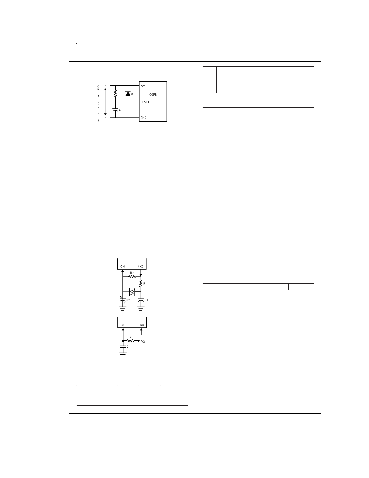
Reset (Continued)
RC>5 x Power Supply Rise Time
FIGURE 6. Recommended Reset Circuit
DS012829-7
Oscillator Circuits
The chip can be driven by a clock input on the CKI input pin
which can be between DC and 10 MHz. The CKO output
clock is on pin G7 (crystal configuration). The CKI input frequency is divided down by 10 to produce the instruction
cycle clock (1/t
Figure 7
CRYSTAL OSCILLATOR
CKI and CKO can be connected to make a closed loop crystal (or resonator) controlled oscillator.
Table 1
standard crystal values.
R/C OSCILLATOR
By selecting CKI as a single pin oscillator input, a single pin
R/C oscillatorcircuit can be connected to it. CKO is available
as a general purpose input, and/or HALT restart input.
Table 2
functions of the component (R and C) values.
FIGURE 7. Crystal and R/C Oscillator Diagrams
TABLE 1. Crystal Oscillator Configuration, T
R1 R2 C1 C2 CKI Freq Conditions
(kΩ)(MΩ) (pF) (pF) (MHz)
0 1 30 30–36 10 V
).
c
shows the Crystal and R/C oscillator diagrams.
shows the component values required for various
shows the variation in the oscillator frequencies as
DS012829-8
DS012829-9
=
25˚C
A
=
5V
CC
R1 R2 C1 C2 CKI Freq Conditions
(kΩ)(MΩ) (pF) (pF) (MHz)
0 1 30 30–36 4 V
0 1 200 100–150 0.455 V
TABLE 2. RC Oscillator Configuration, T
=
5V
CC
=
2.5V
CC
=
25˚C
A
R C CKI Freq Instr. Cycle Conditions
(kΩ) (pF) (MHz) (µs)
3.3 82 2.2 to 2.7 3.7 to 4.6 V
5.6 100 1.1 to 1.3 7.4 to 9.0 V
6.8 100 0.9 to 1.1 8.8 to 10.8 V
Note: 3k ≤ R ≤ 200k
50 pF ≤ C ≤ 200 pF
=
5V
CC
=
5V
CC
=
5V
CC
CONTROL REGISTERS
CNTRL Register (Address X'00EE)
T1C3 T1C2 T1C1 T1C0 MSEL IEDG SL1 SL0
Bit 7 Bit 0
The Timer1 (T1) and MICROWIRE/PLUS control register
contains the following bits:
T1C3 Timer T1 mode control bit
T1C2 Timer T1 mode control bit
T1C1 Timer T1 mode control bit
T1C0 Timer T1 Start/Stop control in timer
modes 1 and 2, T1 Underflow Interrupt
Pending Flag in timer mode 3
MSEL Selects G5 and G4 as MICROWIRE/PLUS
IEDG External interrupt edge polarity select
SL1 & SL0 Select the MICROWIRE/PLUS clock divide
PSW Register (Address X'00EF)
HC C T1PNDA T1ENA EXPND BUSY EXEN GIE
Bit 7 Bit 0
The PSW register contains the following select bits:
HC Half Carry Flag
C Carry Flag
T1PNDA Timer T1 Interrupt Pending Flag (Autoreload
T1ENA Timer T1 Interrupt Enable for Timer Underflow
EXPND External interrupt pending
BUSY MICROWIRE/PLUS busy shifting flag
EXEN Enable external interrupt
GIE Global interrupt enable (enables interrupts)
The Half-Carry flag isalso affectedby all the instructions that
affect the Carry flag. The SC (Set Carry) and R/C (Reset
Carry) instructions will respectively set orclear boththe carry
flags. In addition to the SC and R/C instructions, ADC,
SUBC, RRC and RLC instructions affect the Carry and Half
Carry flags.
signals SK and SO respectively
(0 = Rising edge, 1 = Falling edge)
by (00 = 2, 01 = 4, 1x = 8)
RA in mode 1, T1 Underflow in Mode 2, T1A
capture edge in mode 3)
or T1A Input capture edge
www.national.com 18
Page 19
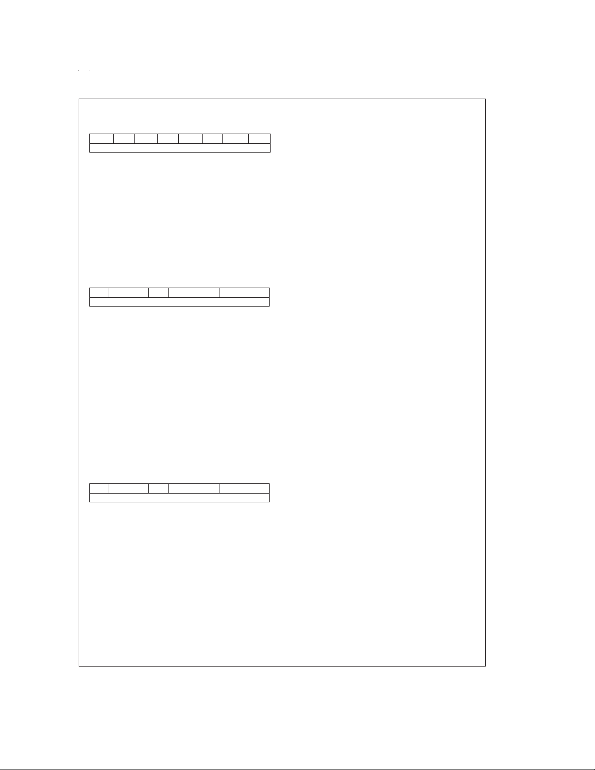
CONTROL REGISTERS (Continued)
ICNTRL Register (Address X'00E8)
Reserved LPEN T0PND T0EN µWPND µWEN T1PNDB T1ENB
Bit 7 Bit 0
The ICNTRL register contains the following bits:
Reserved This bit is reserved and should be zero
LPEN L Port Interrupt Enable (Multi-Input Wakeup/
Interrupt)
T0PND Timer T0 Interrupt pending
T0EN Timer T0 Interrupt Enable (Bit 12 toggle)
µWPND MICROWIRE/PLUS interrupt pending
µWEN Enable MICROWIRE/PLUS interrupt
T1PNDB Timer T1 Interrupt Pending Flag for T1B cap-
ture edge
T1ENB Timer T1 Interrupt Enable for T1B Input cap-
ture edge
T2CNTRL Register (Address X'00C6)
T2C3 T2C2 T2C1 T2C0 T2PNDA T2ENA T2PNDB T2ENB
Bit 7 Bit 0
The T2CNTRL control register contains the following bits:
T2C3 Timer T2 mode control bit
T2C2 Timer T2 mode control bit
T2C1 Timer T2 mode control bit
T2C0 Timer T2 Start/Stop control in timer
modes 1 and 2, T2 Underflow Interrupt Pend-
ing Flag in timer mode 3
T2PNDA Timer T2 Interrupt Pending Flag (Autoreload
RA in mode 1, T2 Underflow in mode 2, T2A
capture edge in mode 3)
T2ENA Timer T2 Interrupt Enable for Timer Underflow
or T2A Input capture edge
T2PNDB Timer T2 Interrupt Pending Flag for T2B cap-
ture edge
T2ENB Timer T2 Interrupt Enable for Timer Underflow
or T2B Input capture edge
Note: The T2CNTRL register is not available on the CS series.
T3CNTRL Register (Address X'00B6)
T3C3 T3C2 T3C1 T3C0 T3PNDA T3ENA T3PNDB T3ENB
Bit 7 Bit 0
The T3CNTRL control register contains the following bits:
T3C3 Timer T3 mode control bit
T3C2 Timer T3 mode control bit
T3C1 Timer T3 mode control bit
T3C0 Timer T3 Start/Stop control in timer
modes 1 and 2, T3 Underflow Interrupt Pend-
ing Flag in timer mode 3
T3PNDA Timer T3 Interrupt Pending Flag (Autoreload
RA in mode 1, T3 Underflow in mode 2, T3A
capture edge in mode 3)
T3ENA Timer T3 Interrupt Enable for Timer Underflow
or T3A Input capture edge
T3PNDB Timer T3 Interrupt Pending Flag for T3B cap-
ture edge
T3ENB Timer T3 Interrupt Enable for Timer Underflow
or T3B Input capture edge
Note: The T3CNTRL regoster os mpt avao;ab;e pm tje CS series.
Timers
These devices contain a very versatile set of timers (T0, T1,
T2, T3 for all except the CS series, which only use T0 and
T1). All timers and associated autoreload/capture registers
power up containing random data.
TIMER T0 (IDLE TIMER)
The device supports applications that require maintaining
real time and low power with the IDLE mode. This IDLE
mode support is furnished by the IDLE timer T0, which is a
16-bit timer.The TimerT0 runs continuously at the fixed rate
of the instruction cycle clock, t
write to the IDLE Timer T0, which is a count down timer.
The Timer T0 supports the following functions:
j
Exit out of the Idle Mode (See Idle Mode description)
j
WATCHDOG logic (See WATCHDOG description)
j
Start up delay out of the HALT mode
The IDLE Timer T0 can generate an interrupt when the thirteenth bit toggles. This toggle is latched into the T0PND
pending flag, and will occur every 4 ms at the maximum
clock frequency (t
terrupt from the thirteenth bit of Timer T0 to be enabled or
=
1 µs). Acontrol flagT0EN allows the in-
c
disabled. Setting T0EN will enable the interrupt, while resetting it will disable the interrupt.
TIMER T1, TIMER T2 AND TIMER T3
These devices can have a set of up to three powerful timer/
counter blocks, T1, T2 and T3. The associated features and
functioning of a timer block are described by referring to the
timer block Tx. Since the three timer blocks, T1, T2 and T3
are identical, all comments are equally applicable to any of
the three timer blocks.
Each timer block consists of a 16-bit timer, Tx, and two supporting 16-bit autoreload/capture registers, RxA and RxB.
Each timer block has two pins associated with it, TxA and
TxB. The pin TxA supports I/O required by the timer block,
while the pin TxB is an input to the timer block. The powerful
and flexible timer block allows the device toeasily performall
timer functions with minimal software overhead. The timer
block has three operating modes: Processor Independent
PWM mode, External Event Counter mode, and Input Capture mode.
The controlbits TxC3,TxC2, and TxC1 allow selectionof the
different modes of operation.
Mode 1. Processor Independent PWM Mode
As the name suggests, this mode allows the device to generate a PWM signal with very minimal user intervention. The
user only has to define the parameters of the PWM signal
(ON time and OFF time). Once begun, the timer block will
continuously generate the PWM signal completely independent of the microcontroller. The user software services the
timer block only when the PWM parameters require updating.
In this mode the timer Tx counts down at a fixed rate of t
Upon every underflow the timer is alternately reloaded with
the contents of supporting registers, RxA and RxB. The very
first underflow of the timer causes the timer to reload from
the register RxA. Subsequent underflows cause the timer to
be reloaded from the registers alternately beginning with the
register RxB.
The Tx Timer control bits, TxC3, TxC2 and TxC1 set up the
timer for PWM mode operation.
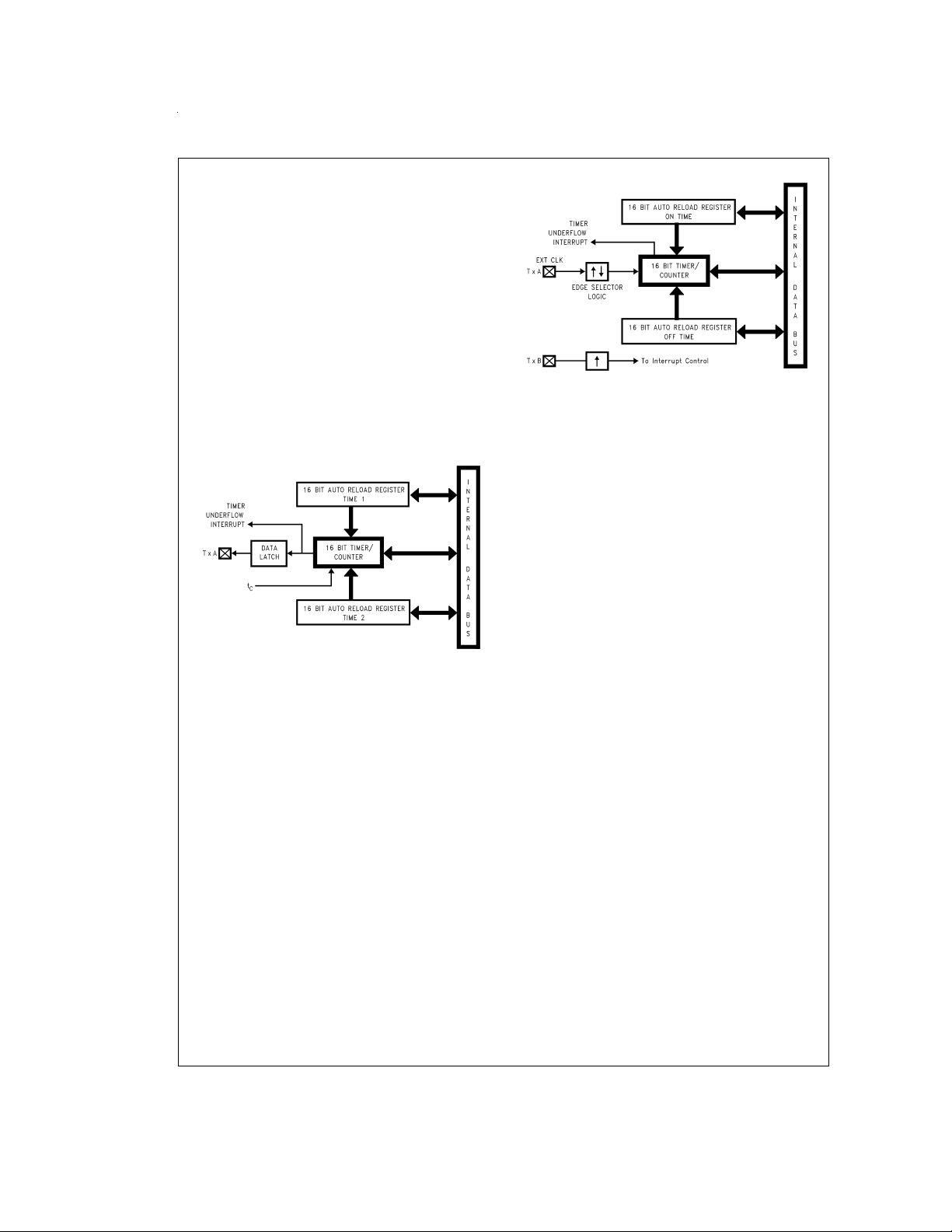
Figure 8
shows a block diagram of the timer in PWM mode.
. The user cannot read or
c
www.national.com19
.
c
Page 20
Timers (Continued)
The underflows can beprogrammed to toggle the TxA output
pin. The underflows can also be programmed to generate interrupts.
Underflows from the timer are alternately latched into two
pending flags, TxPNDA and TxPNDB. The user must reset
these pending flags under software control. Two control enable flags, TxENA and TxENB, allow the interrupts from the
timer underflow to be enabled or disabled. Setting the timer
enable flag TxENA will cause an interrupt when a timer underflow causes the RxA registerto bereloaded intothe timer.
Setting the timer enable flag TxENB will cause an interrupt
when a timer underflow causes the RxB register to be reloaded into the timer. Resetting the timer enable flags will
disable the associated interrupts.
Either or both of the timer underflow interrupts may be enabled. This gives the user the flexibility of interrupting once
per PWM period on either the rising or falling edge of the
PWM output. Alternatively, the user may choose to interrupt
on both edges of the PWM output.
DS012829-10
FIGURE 8. Timer in PWM Mode
Mode 2. External Event Counter Mode
This mode is quite similar to the processor independent
PWM modedescribed above. The main differenceis that the
timer,Tx, is clocked by the input signal from the TxA pin.The
Tx timer control bits, TxC3, TxC2 and TxC1 allow the timer to
be clocked either on a positive or negative edge from the
TxA pin. Underflows from the timer are latched into theTxPNDA pending flag. Setting the TxENAcontrol flag will cause
an interrupt when the timer underflows.
In this mode the input pin TxB can be used as an independent positiveedge sensitive interruptinput if the TxENB control flag is set. The occurrence of a positive edge on the TxB
input pin is latched into the TxPNDB flag.
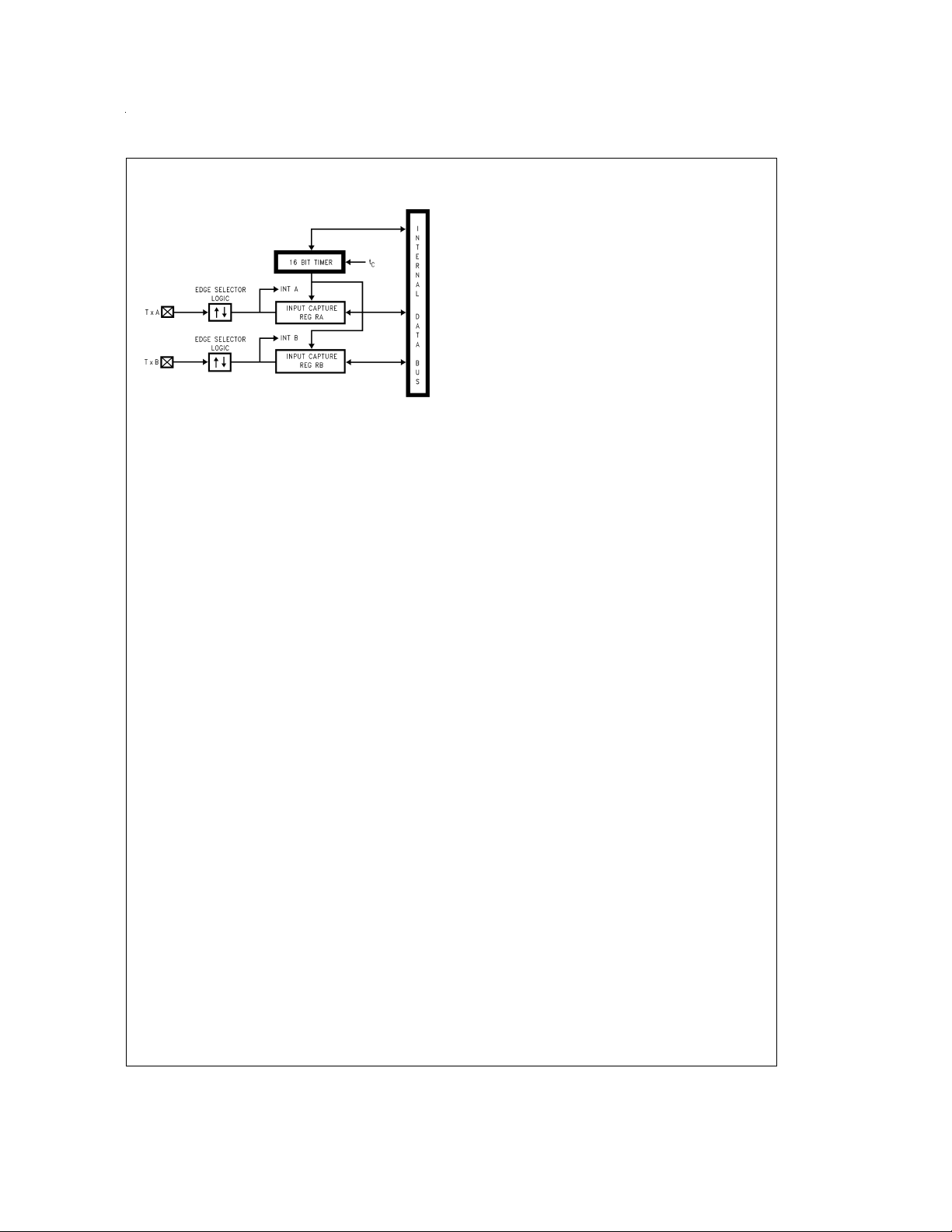
Figure 9
Event Counter mode.
Note: The PWM output isnotavailable in this mode sincetheTxApin is being
shows a block diagram of the timer in External
used as the counter input clock.
DS012829-11
FIGURE 9. Timer in External Event Counter Mode
Mode 3. Input Capture Mode
The device can precisely measure external frequencies or
time external events by placing the timer block, Tx, in the input capture mode.
In this mode, the timerTx is constantly running at the fixed t
rate. The two registers, RxA and RxB, act as capture registers. Each register acts in conjunctionwith apin. The register
RxAacts inconjunction withthe TxA pinand theregister RxB
acts in conjunction with the TxB pin.
The timer value gets copied over into the register when a
trigger event occurs on its corresponding pin. Control bits,
TxC3, TxC2 and TxC1, allow the trigger events to be specified either as a positive or a negative edge. The trigger condition for each input pin can be specified independently.
The trigger conditions can also be programmed to generate
interrupts. The occurrence of the specified trigger condition
on the TxA and TxB pins will be respectively latched into the
pending flags, TxPNDA and TxPNDB. The control flag TxENA allows the interrupt on TxA to be either enabled or disabled. Setting the TxENA flagenables interruptsto begenerated when the selected trigger condition occurs on the TxA
pin. Similarly, the flag TxENB controls the interrupts from the
TxB pin.
Underflows from the timer can also be programmed to generate interrupts. Underflows are latched into the timer TxC0
pending flag (the TxC0 control bit serves as the timer underflow interrupt pending flag in the Input Capture mode). Consequently, the TxC0 control bit should be reset when entering the Input Capture mode. The timer underflow interrupt is
enabled with the TxENA control flag. When a TxA interrupt
occurs in the Input Capture mode, the user must check both
the TxPNDA and TxC0 pending flags in order to determine
whether a TxA input capture or a timer underflow (or both)
caused the interrupt.
Figure 10
shows a block diagram of the timer in Input Cap-
ture mode.
c
www.national.com 20
Page 21
Timers (Continued)
DS012829-12
FIGURE 10. Timer in Input Capture Mode
TIMER CONTROL FLAGS
The control bits and their functions are summarized below.
TxC3 Timer mode control
TxC2 Timer mode control
TxC1 Timer mode control
TxC0 Timer Start/Stop control in Modes 1 and 2 (Pro-
TxPNDA Timer Interrupt Pending Flag
TxENA Timer Interrupt Enable Flag
TxPNDB Timer Interrupt Pending Flag
TxENB Timer Interrupt Enable Flag
cessor Independent PWM and External Event
Counter), where 1 = Start, 0 = Stop
Timer Underflow Interrupt Pending Flag in
Mode 3 (Input Capture)
1 = Timer Interrupt Enabled
0 = Timer Interrupt Disabled
1 = Timer Interrupt Enabled
0 = Timer Interrupt Disabled
www.national.com21
Page 22
Timers (Continued)
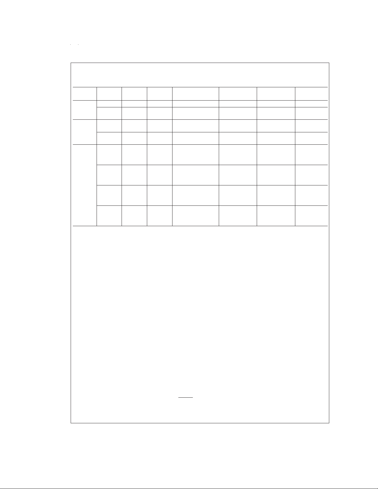
The timer mode control bits (TxC3, TxC2 and TxC1) are detailed below:
Mode TxC3 TxC2 TxC1 Description
1 0 1 PWM: TxA Toggle Autoreload RA Autoreload RB t
1
1 0 0 PWM: No TxA
Toggle
0 0 0 External Event
2
0 0 1 External Event
Counter
Counter
0 1 0 Captures: Pos. TxA Edge Pos. TxB Edge t
TxA Pos. Edge or Timer
TxB Pos. Edge Underflow
1 1 0 Captures: Pos. TxA Neg. TxB t
TxA Pos. Edge Edge or Timer Edge
3
0 1 1 Captures: Neg. TxA Neg. TxB t
TxB Neg. Edge Underflow
TxA Neg. Edge Edge or Timer Edge
TxB Neg. Edge Underflow
1 1 1 Captures: Neg. TxA Neg. TxB t
TxA Neg. Edge Edge or Timer Edge
TxB Neg. Edge Underflow
Power Save Modes
The device offers the user two power save modes of operation: HALT and IDLE. In the HALT mode, all microcontroller
activities are stopped. In the IDLE mode, the on-board oscillator circuitry and timer T0 are active but all other microcontroller activities are stopped. In either mode, all on-board
RAM, registers, I/O states, and timers (with the exception of
T0) are unaltered.
HALT MODE
The device can be placed in the HALTmode by writing a “1”
to the HALT flag (G7 data bit). All microcontroller activities,
including the clock and timers, are stopped. The WATCHDOG logic on the device is disabled during the HALT mode.
However, the clock monitor circuitry if enabled remains active and will cause the WATCHDOG output pin (WDOUT) to
go low. Ifthe HALTmode is used and the user doesnot want
to activate the WDOUT pin, the Clock Monitor should be disabled after the devicecomes outof reset (resetting the Clock
Monitor control bit withthe firstwrite to the WDSVR register).
In the HALT mode, the power requirements of the device are
minimal and the applied voltage (V
=
V
2.0V) without altering the state of the machine.
r(Vr
The device supports three different ways of exiting the HALT
mode. The first method of exiting the HALTmode is with the
Multi-Input Wakeup feature on the L port. The second
method is with a low to high transition on the CKO (G7) pin.
This method precludes theuse of the crystal clock configuration (since CKO becomes a dedicated output), and so may
only be used with an RC clock configuration. The third
method of exiting the HALT mode is by pulling the RESET
pin low.
Since a crystal or ceramic resonator may be selected as the
oscillator, the Wakeup signal is not allowed to start the chip
www.national.com 22
) may be decreased to
CC
Interrupt A
Source
Autoreload RA Autoreload RB
Timer
Underflow
Timer
Underflow
Interrupt B
Source
Timer
Counts On
C
t
C
Pos. TxB Edge Pos. TxA
Edge
Pos. TxB Edge Pos. TxA
Edge
C
C
C
C
running immediately since crystal oscillators and ceramic
resonators have a delayed start up time to reach full amplitude and frequency stability. The IDLE timer is used to generate a fixed delay to ensure that the oscillator has indeed
stabilized before allowing instruction execution. In this case,
upon detecting a valid Wakeup signal, only the oscillator circuitry is enabled. The IDLE timer is loaded with a value of
256 and is clocked with the t
clock is derived by dividing the oscillator clock down by a fac-
instruction cycle clock. The t
c
tor of 10. The Schmitt trigger following the CKI inverter on
the chip ensures that the IDLE timer is clocked only when the
oscillator has a sufficiently large amplitude to meet the
Schmitt trigger specifications.This Schmitt trigger is not part
of the oscillator closed loop. The startup timeout from the
IDLE timer enables the clock signals to be routed to the rest
of the chip.
If an RC clock option is being used, the fixed delay is introduced optionally.A control bit, CLKDLY, mapped as configuration bit G7, controls whether the delay is to be introduced
or not. The delay is included if CLKDLYis set, and excluded
if CLKDLY is reset. The CLKDLY bit is cleared on reset.
The device has two mask options associated with the HALT
mode. The first mask option enables the HALT mode feature,
while thesecond mask option disables the HALT mode. With
the HALT mode enable mask option, the device will enter
and exit the HALT mode as described above. With the HALT
disable mask option, the device cannot be placed in the
HALTmode (writing a “1”to the HALT flag will have no effect,
the HALT flag will remain “0”).
IDLE MODE
The device is placed in the IDLE mode by writing a “1” to the
IDLE flag(G6 data bit).In this mode,all activities, exceptthe
associated on-board oscillator circuitry and the IDLE Timer
T0, are stopped. The power supply requirements of the
c
Page 23
Power Save Modes (Continued)
micro-controller in this mode of operation are typically
around 30%of normal power requirement of the microcontroller.
As with the HALT mode, the device can be returned to normal operation with areset, or with a Multi-InputWakeup from
the L Port. Alternately, the microcontroller resumes normal
operation fromthe IDLE mode when the thirteenth bit (representing 4.096 ms at internal clock frequency of 10 MHz, t
1 µs) of the IDLE Timer toggles.
This toggle condition of the thirteenth bit of the IDLE Timer
T0 is latched into the T0PND pending flag.
The user has the option of being interrupted with a transition
on the thirteenth bit of the IDLE Timer T0. The interrupt can
be enabled or disabled via the T0EN control bit. Setting the
T0EN flag enables the interrupt and vice versa.
The user can enter the IDLE mode with the Timer T0 interrupt enabled. In this case, when the T0PND bit gets set, the
c
device will first execute the TimerT0 interrupt service routine
and then return to the instruction following the “Enter Idle
Mode” instruction.
Alternatively, the user can enter the IDLE mode with the
IDLE Timer T0 interrupt disabled. In this case, the device will
resume normal operation with the instruction immediately
following the “Enter IDLE Mode” instruction.
Note: It is necessary to program two NOP instructions following both the set
HALT mode and set IDLE mode instructions. These NOP instructions
=
are necessary to allow clock resynchronization following the HALT or
IDLE modes.
Multi-Input Wakeup
The Multi-Input Wakeupfeature isued toreturn (wakeup) the
device from either the HALT or IDLE modes. Alternately
Multi-Input Wakeup/Interrupt feature may also be used to
generate up to 8 edge selectable external interrupts.
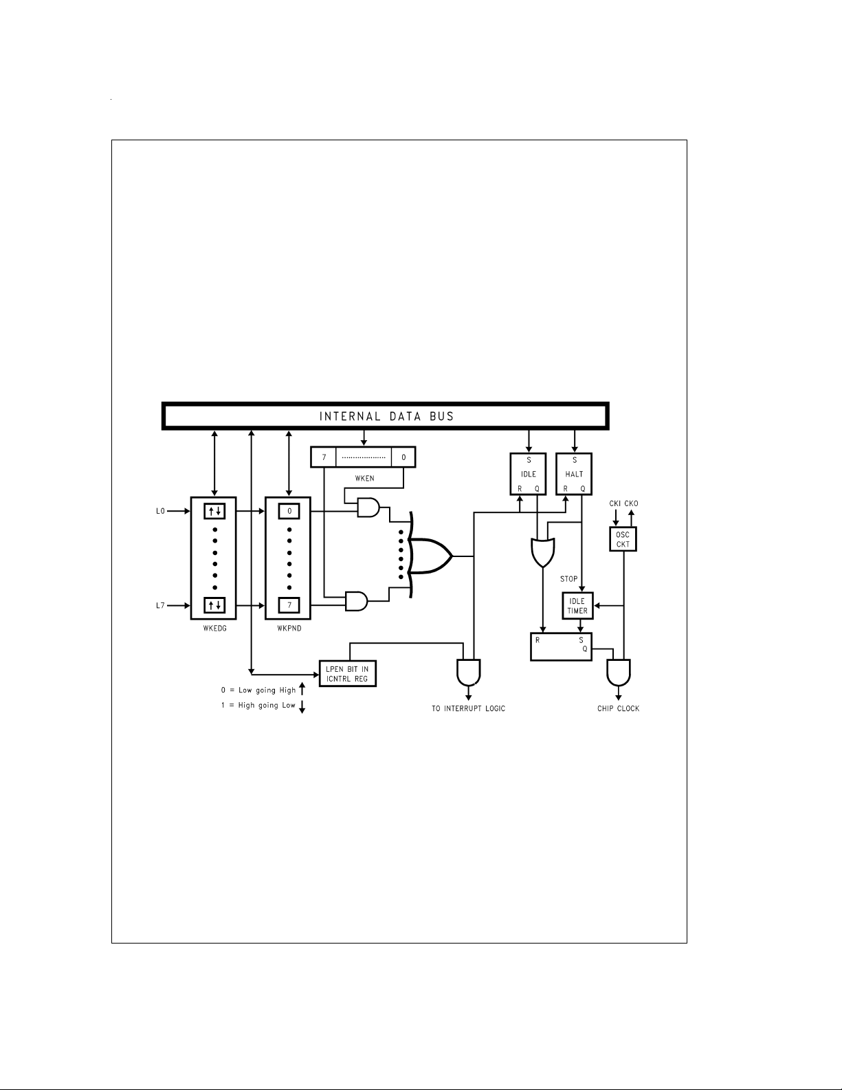
Figure 11
shows the Multi-Input Wakeup logic.
FIGURE 11. Multi-Input Wake Up Logic
The Multi-Input Wakeup feature utilizes the L Port. The user
selects which particular L port bit (or combination of L Port
bits) will cause the device to exit the HALT or IDLE modes.
The selectionis done throughthe Register WKEN. The Register WKEN is an 8-bit read/write register, which contains a
control bit for every L port bit. Setting a particular WKEN bit
enables a Wakeup from the associated L port pin.
The user can select whether the trigger condition on the selected L Port pin is going to be either a positive edge (low to
high transition) or a negative edge (high to low transition).
This selection is made via the Register WKEDG, which is an
8-bit control register with a bit assigned to each L Port pin.
Setting the control bit will select the trigger condition to be a
negative edge on that particular L Port pin. Resetting the bit
selects the trigger condition to be a positive edge. Changing
DS012829-13
an edge select entails several steps in order to avoid a
Wakeup condition as a result of the edge change. First, the
associated WKEN bit should be reset, followed by the edge
select change in WKEDG. Next, the associated WKPND bit
should be cleared, followed by the associated WKEN bit being re-enabled.
An example may serve to clarify thisprocedure. Suppose we
wish to change the edge select from positive (low goinghigh)
to negative (high going low) for L Port bit 5, where bit 5 has
previously been enabled for an input interrupt. The program
would be as follows:
RBIT 5, WKEN ; Disable MIWU
SBIT 5, WKEDG ; Change edge polarity
RBIT 5, WKPND ; Reset pending flag
SBIT 5, WKEN ; Enable MIWU
www.national.com23
Page 24

Multi-Input Wakeup (Continued)
If the L port bits have been used as outputs and then
changed to inputs with Multi-Input Wakeup/Interrupt,a safety
procedure should also be followed to avoid wakeup conditions. After the selected L port bits have been changed from
output to input but before the associated WKEN bits are enabled, the associated edge select bits in WKEDG should be
set or reset for the desired edge selects, followed by the associated WKPND bits being cleared.
This same procedure should be used following reset, since
the L port inputs are left floating as a result of reset.
The occurrence of the selected trigger condition for
Multi-Input Wakeup is latched into a pending register called
WKPND. The respective bits of the WKPND register will be
set on the occurrence of the selected trigger edge on the corresponding Port L pin. The user has the responsibility of
clearing these pending flags. Since WKPND is a pending
register for the occurrence of selected wakeup conditions,
the device will not enter the HALTmode if any Wakeup bit is
both enabled and pending. Consequently, the user must
clear the pending flags before attempting to enter the HALT
mode.
WKEN, WKPND and WKEDG are all read/write registers,
and are cleared at reset.
PORT L INTERRUPTS
Port L provides the user with an additional eight fully selectable, edgesensitive interrupts which are all vectored into the
same service subroutine.
The interrupt from Port L shares logic with the wake up circuitry.The register WKEN allows interrupts from Port L to be
individually enabledor disabled. The register WKEDGspecifies the trigger condition to be either a positive or a negative
edge. Finally, the register WKPND latches in the pending
trigger conditions.
The GIE (Global Interrupt Enable) bit enables the interrupt
function.
A control flag, LPEN, functions as a global interrupt enable
for Port L interrupts. Setting the LPEN flag will enable interrupts and vice versa. A separate global pending flag is not
needed since the register WKPND is adequate.
Since Port L is also used for waking the device out of the
HALTor IDLE modes, the user can elect to exit the HALT or
IDLE modes either withor without the interrupt enabled.If he
elects to disable the interrupt, then the device will restart execution from the instruction immediately following the instruction that placed the microcontroller in the HALT or IDLE
modes. In the other case, the device will first execute the interrupt service routine and then revert to normal operation.
(See HALT MODE for clock option wakeup information.)
The Wakeup signal will not start the chip running immediately since crystal oscillators or ceramicresonators havea finite start up time. The IDLE Timer (T0) generates a fixed delay to ensure that the oscillator has indeed stabilized before
allowing the device to execute instructions. In this case,
upon detecting a valid Wakeup signal, only the oscillator circuitry andthe IDLE Timer T0 are enabled. TheIDLE Timeris
loaded with a value of 256 and is clocked from the t
tion cycle clock. The t
oscillator clock by a factor of 10. A Schmitt trigger following
the CKI on-inverter ensures that the IDLE timer is clocked
only when the oscillator has a sufficiently large amplitude to
meet the Schmitt trigger specifications. This Schmitt trigger
is not part of the oscillator closed loop. The start-up time-out
from theIDLE timer enablesthe clock signalsto be routedto
the rest of the chip.
If the RC clock option is used, the fixed delay is under software control.A control flag, CLKDLY, in the G7 configuration
bit allows the clock start up delay to be optionally inserted.
Setting CLKDLY flag high will cause clock start up delay to
be inserted and resetting it will exclude the clock start up delay. The CLKDLY flag high will cause clock start up delay.
The CLKDLY flag is cleared during reset, so the clock start
up delay is not present following reset with the RC clock options.
clock is derived by dividing down the
c
instruc-
c
USART
The device contains a full-duplex software programmable
USART. The USART (
register, a receive shift register and seven addressable registers, as follows: a transmit buffer register (TBUF), a receiver buffer register (RBUF), a USART control and status
register (ENU), a USART receive control and status register
(ENUR), a USART interrupt and clock source register
(ENUI), a prescaler select register (PSR) and baud (BAUD)
register.The ENU register contains flags for transmit and receive functions; this register also determines the length of
the data frame (7, 8 or 9 bits), the value of the ninth bit in
transmission, and parity selection bits. The ENUR register
flags framing, data overrun and parity errors while the USART is receiving.
Other functions of the ENUR register include saving the
ninth bit received in the data frame, enabling or disabling the
USART’s attention mode of operation and providing additional receiver/transmitter status information via RCVG and
XMTG bits. The determination of an internal orexternal clock
source is done by the ENUI register,as well as selecting the
number of stop bits and enabling or disabling transmit and
receive interrupts. A control flag in this register can also select the USART mode of operation: asynchronous or
synchronous.
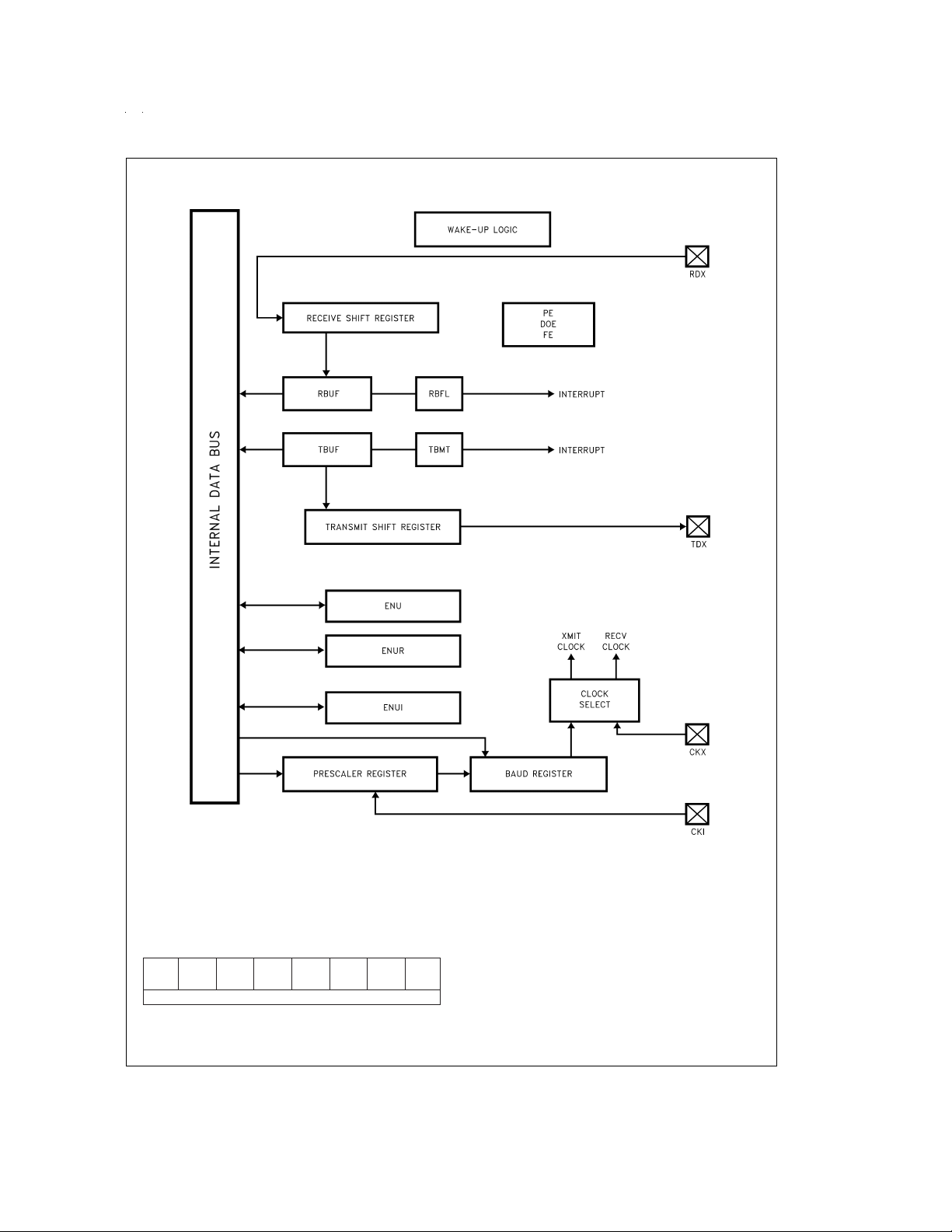
Figure 12
) consists of a transmit shift
www.national.com 24
Page 25
USART (Continued)
FIGURE 12. USART Block Diagram
USART CONTROL AND STATUS REGISTERS
The operation of the USART is programmed through three
registers: ENU, ENUR and ENUI.
DESCRIPTION OF USART REGISTER BITS
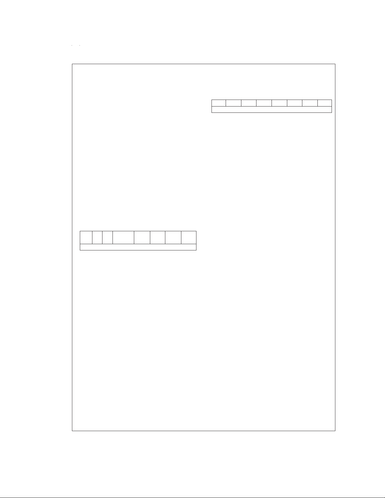
ENU-USART Control and Status Register (Address at 0BA)
PEN PSEL1 XBIT9/ CHL1 CHL0 ERR RBFL TBMT
PSEL0
Bit 7 Bit 0
PEN: This bit enables/disables Parity (7- and 8-bit modes
only). Read/Write, cleared on reset.
PEN = 0 Parity disabled.
DS012829-14
PEN = 1 Parity enabled.
PSEL1, PSEL0: Parity select bits. Read/Write, cleared on
reset.
PSEL1 = 0, PSEL0 = 0 Odd Parity (if Parity enabled)
PSEL1 = 0, PSEL0 = 1 Even Parity (if Parity enabled)
PSEL1 = 1, PSEL0 = 0 Mark(1) (if Parity enabled)
PSEL1 = 1, PSEL0 = 1 Space(0) (if Parity enabled)
XBIT9/PSEL0: Programs the ninth bit for transmission when
the USART is operating with nine data bits per frame. For
seven oreight data bitsper frame, thisbit in conjunctionwith
PSEL1 selects parity. Read/Write, cleared on reset.
www.national.com25
Page 26
USART (Continued)
CHL1, CHL0: These bits select the character frame format.
Parity is not included and is generated/verified by hardware.
Read/Write, cleared on reset.
CHL1 = 0, CHL0 = 0 The frame contains eight data bits.
CHL1 = 0, CHL0 = 1 The frame contains seven data
bits.
CHL1 = 1, CHL0 = 0 The frame contains nine data bits.
CHL1 = 1, CHL0 = 1 Loopback Mode selected. Trans-
mitter output internally looped back
to receiver input. Nine bit framing
format is used.
ERR: This bit is a global USART error flag which gets set if
any or a combination of the errors (DOE, FE, PE) occur.
Read only;it cannot be written by software, cleared on reset.
RBFL: This bit is set when the USART has received a complete character and has copied it into the RBUF register. It is
automatically reset when software reads the character from
RBUF. Read only; it cannot be written by software, cleared
on reset.
TBMT: This bit is set when the USART transfers a byte of
data from the TBUF register into the TSFT register for transmission. It is automatically reset when software writes into
the TBUF register. Read only, bit is set to “one” on reset; it
cannot be written by software.
ENUR-USART Receive Control and Status Register
(Address at 0BB)
DOE FE PE Reserved RBIT9 ATTN XMTG RCVG
(Note 12)
Bit 7 Bit 0
Note 12: Bit is reserved for future use. User must set to zero.
DOE: Flags a Data Overrun Error. Read only, cleared on
read, cleared on reset.
DOE = 0 Indicates no Data Overrun Error has been de-
tected since the last time the ENUR register
was read.
DOE = 1 Indicates the occurrence of a Data Overrun Er-
ror.
FE: Flags a Framing Error. Read only, cleared on read,
cleared on reset.
FE = 0 Indicates no Framing Error has been detected
since the last time the ENUR register was read.
FE = 1 Indicates the occurrence of a Framing Error.
PE: Flagsa Parity Error. Read only, cleared on read, cleared
on reset.
PE = 0 Indicates no Parity Error has been detected since
the last time the ENUR register was read.
PE = 1 Indicates the occurrence of a Parity Error.
SPARE:Reserved for futureuse. Read/Write, cleared on re-
set.
RBIT9: Contains the ninth data bit received when the US-
ART is operating with nine data bits per frame. Read only,
cleared on reset.
ATTN: ATTENTION Mode is enabled while this bit is set.
This bit is clearedautomatically on receiving a character with
data bit nine set. Read/Write, cleared on reset.
XMTG: This bit is set to indicate that the USART is transmitting. It gets reset at theend ofthe last frame (end of last Stop
bit). Read only, cleared on reset.
RCVG: This bit is set high whenever a framing error occurs
and goes low when RDX goes high. Read only, cleared on
reset.
ENUI-USART Interrupt and Clock Source Register
(Address at 0BC)
STP2 STP78 ETDX SSEL XRCLK XTCLK ERI ETI
Bit 7 Bit 0
STP2: Thisbit programs thenumber of Stopbits to be transmitted. Read/Write, cleared on reset.
STP2 = 0 One Stop bit transmitted.
STP2 = 1 Two Stop bits transmitted.
STP78: This bit is set to program the last Stop bit to be 7/8th
of a bit in length. Read/Write, cleared on reset.
ETDX: TDX (USART Transmit Pin) is the alternate function
assigned to Port L pin L2; it is selected by setting ETDX bit.
To simulate line break generation, software should reset
ETDX bit and output logic zero to TDX pin through Port L
data and configuration registers. Read/Write, cleared on reset.
SSEL: USART mode select. Read/Write, cleared on reset.
SSEL = 0 Asynchronous Mode.
SSEL = 1 Synchronous Mode.
XRCLK: This bit selects the clock source for the receiver
section. Read/Write, cleared on reset.
XRCLK = 0 The clock source is selected through the
PSR and BAUD registers.
XRCLK = 1 Signal on CKX (L1) pin is used as the clock.
XTCLK: This bit selects the clock source for the transmitter
section. Read/Write, cleared on reset.
XTCLK = 0 The clock source is selected through the
PSR and BAUD registers.
XTCLK = 1 Signal on CKX (L1) pin is used as the clock.
ERI: This bit enables/disables interrupt from the receiver
section. Read/Write, cleared on reset.
ERI = 0 Interrupt from the receiver is disabled.
ERI = 1 Interrupt from the receiver is enabled.
ETI: This bit enables/disables interrupt from the transmitter
section. Read/Write, cleared on reset.
ETI = 0 Interrupt from the transmitter is disabled.
ETI = 1 Interrupt from the transmitter is enabled.
Associated I/O Pins
Data is transmitted on the TDX pin and received on the RDX
pin. TDX is the alternate function assigned to Port L pin L2;
it is selected by setting ETDX (in the ENUI register) to one.
RDX is an inherent function of Port L pin L3, requiring no
setup.
The baud rate clock for the USART can be generated
on-chip, or can be taken from an external source. Port L pin
L1 (CKX) is the external clock I/O pin. The CKX pin can be
either an input or an output, as determined by Port L Configuration and Data registers (Bit 1).As an input, it accepts a
clock signal which may be selected to drive the transmitter
and/or receiver. As an output, it presents the internal Baud
Rate Generator output.
www.national.com 26
Page 27

USART Operation
The USART has two modes of operation: asynchronous
mode and synchronous mode.
ASYNCHRONOUS MODE
This mode is selected by resetting the SSEL (in the ENUI
register) bit to zero. The input frequency to the USART is 16
times the baud rate.
The TSFT and TBUF registers double-buffer data for transmission. While TSFT is shifting out the current character on
the TDX pin, the TBUF register may be loaded by software
with the next byte to be transmitted. When TSFT finishes
transmitting the current character the contents of TBUF are
transferred to the TSFT register and the Transmit Buffer
Empty Flag (TBMT in the ENU register) is set. The TBMT
flag is automatically reset by the USART when software
loads a new character into the TBUF register. There is also
the XMTG bit which is set to indicate that the USART is
transmitting. This bit gets reset at the end of the last frame
(end of last Stop bit). TBUF is a read/write register.
The RSFT and RBUF registers double-buffer data being received. The USART receiver continually monitors the signal
on the RDX pin for a low level to detect the beginning of a
Start bit. Upon sensing this low level, it waits for half a bit
time and samples again. If the RDX pin is still low, the receiver considers this to be avalid Startbit, and the remaining
bits in the character frame are each sampled a single time, at
the mid-bit position. Serial data input on the RDX pin is
shifted into the RSFT register. Upon receiving the complete
character, the contents of the RSFT register are copied into
the RBUF register and the Received BufferFull Flag (RBFL)
is set. RBFL is automatically reset when software reads the
character from the RBUF register. RBUF is a read only register. There is also the RCVG bit which is set high when a
framing error occurs and goes low once RDX goes high.
TBMT, XMTG, RBFL and RCVG are read only bits.
SYNCHRONOUS MODE
In this mode data is transferred synchronously with the
clock. Datais transmitted onthe rising edge and received on
the falling edge of the synchronous clock.
This mode is selected by setting SSEL bit in the ENUI register. The input frequency to the USART is the same as the
baud rate.
When an external clock input is selected at the CKX pin, data
transmit and receive are performed synchronously with this
clock through TDX/RDX pins.
If datatransmit and receiveare selected withthe CKX pinas
clock output, the device generates the synchronous clock
output at the CKX pin. The internal baud rate generator is
used to produce the synchronous clock. Data transmit and
receive are performed synchronously with this clock.
FRAMING FORMATS
The USART supports several serial framing formats (
13
). The format is selected using control bits in the ENU,
ENUR and ENUI registers.
The firstformat (1, 1a, 1b, 1c) for data transmission(CHL0
1, CHL1=0) consistsof Start bit,seven Data bits(excluding
parity) and 7/8, one or two Stop bits. In applications using
parity, the parity bit is generated and verified by hardware.
The second format (CHL0=0, CHL1=0) consists of one
Start bit, eight Data bits (excluding parity) and 7/8, one or
two Stop bits. Parity bit is generated and verified by hardware.
The thirdformat for transmission(CHL0=0, CHL1=1) consists of one Start bit, nine Data bits and 7/8, one or two Stop
bits. This format also supports the USART “ATTENTION”
feature. When operating in this format, all eight bits of TBUF
and RBUF are usedfor data.The ninthdata bit is transmitted
and received using two bits in the ENU and ENUR registers,
called XBIT9 and RBIT9. RBIT9 is a read only bit. Parity is
not generated or verified in this mode.
For any of the above framing formats, the last Stop bit can
be programmed to be 7/8th of a bit in length. If two Stop bits
are selected and the 7/8th bit is set (selected), the second
Stop bit will be 7/8th of a bit in length.
The parity is enabled/disabledby PEN bit located inthe ENU
register. Parity is selected for 7- and 8-bit modes only. If parity is enabled (PEN=1), the parity selection is then performed by PSEL0 and PSEL1 bits located in the ENU register.
Note that the XBIT9/PSEL0 bit located in the ENU register
serves two mutually exclusive functions. This bit programs
the ninth bit for transmission when the USART is operating
with nine data bits per frame. There is no parity selection in
this framing format. For other framing formats XBIT9 is not
needed and the bitis PSEL0used in conjunction with PSEL1
to select parity.
The frame formats for the receiver differ from the transmitter
in the number of Stop bits required. The receiver only requires one Stop bit in aframe, regardlessof thesetting ofthe
Stop bit selection bits in the control register. Note that an implicit assumption is made for full duplex USART operation
that the framing formats are the same for the transmitter and
receiver.
Figure
=
www.national.com27
Page 28
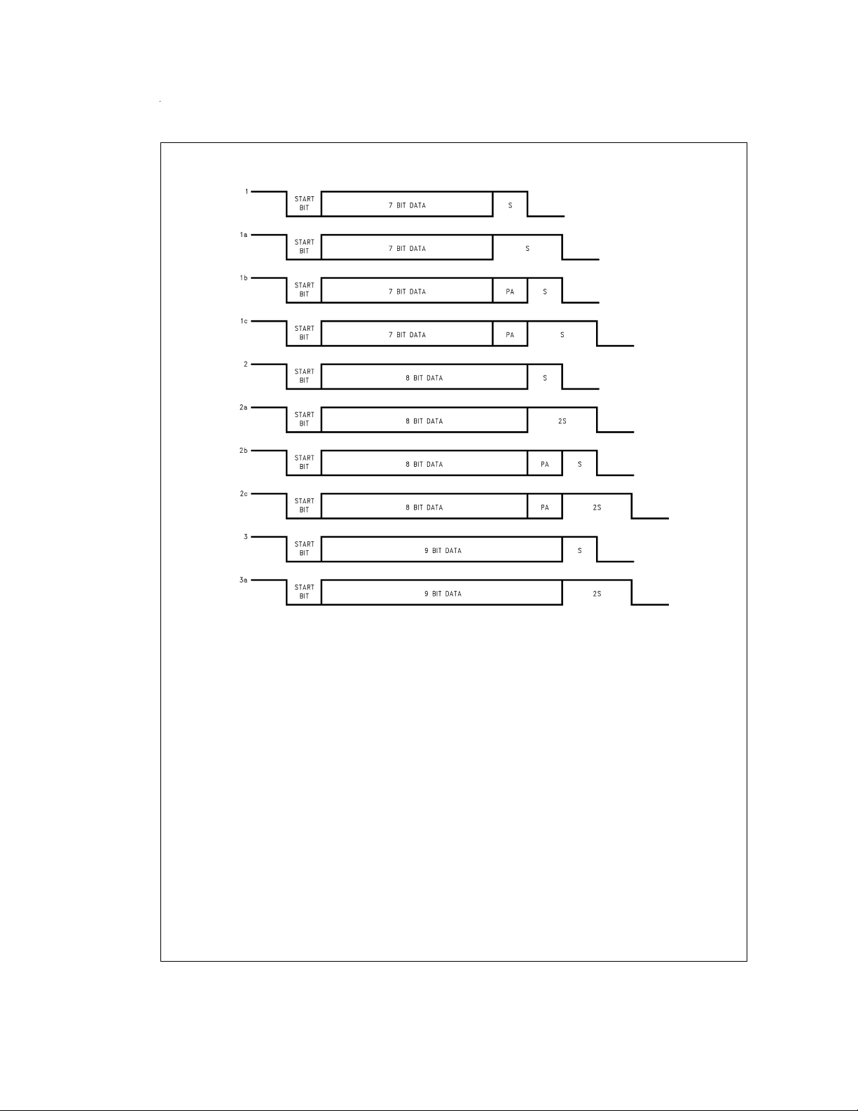
USART Operation (Continued)
FIGURE 13. Framing Formats
USART INTERRUPTS
The USART is capable of generating interrupts. Interrupts
are generated on Receive Buffer Full and Transmit Buffer
Empty. Both interrupts have individual interrupt vectors. Two
bytes of program memory space arereserved for each interrupt vector. The two vectors are located at addresses 0xEC
to 0xEF Hex in the program memory space. The interrupts
can be individually enabled or disabled using Enable Transmit Interrupt (ETI) and Enable Receive Interrupt (ERI) bits in
the ENUI register.
The interrupt from the Transmitter is set pending, and remains pending, as long as both the TBMT and ETI bits are
set. To remove this interrupt, software must either clear the
ETI bit or write to the TBUF register (thus clearing the TBMT
bit).
The interrupt from the receiver is set pending, and remains
pending, as long as both the RBFL and ERI bits are set. To
remove this interrupt, software must either clear the ERI bit
or read from the RBUF register (thus clearing the RBFL bit).
Baud Clock Generation
The clock inputs to the transmitter and receiver sections of
the USART can be individually selected to come either from
an external source at the CKX pin (port L, pin L1) or from a
source selected in the PSR and BAUD registers. Internally,
www.national.com 28
DS012829-15
the basic baud clock is created from the oscillator frequency
through a two-stage divider chain consisting of a 1–16 (increments of 0.5) prescaler and an 11-bit binary counter. (
ure 14
). The divide factors are specified through two read/
write registers shown in
Rate Divisor spills over into the Prescaler Select Register
(PSR). PSR is cleared upon reset.
As shown in
NO CLOCK.This condition is the USART power down mode
where the USART clock is turned off for power saving purpose. The user must also turn the USART clock off when a
different baud rate is chosen.
The correspondences between the 5-bit Prescaler Select
and Prescaler factors are shown in
ways to calculate the two divisor factors, but one particularly
effective method would be to achieve a 1.8432 MHz frequency coming out of the first stage. The 1.8432 MHz prescaler output is thenused to drive the software programmable
baud rate counter to create a 16x clock for the following baud
rates: 110, 134.5, 150, 300, 600, 1200, 1800, 2400, 3600,
4800, 7200, 9600, 19200 and 38400 (
rates may be created by using appropriate divisors. The 16x
clock is then divided by 16 to provide the rate for the serial
shift registers of the transmitter and receiver.
Table6
Figure 15
. Note that the 11-bit Baud
, a Prescaler Factor of 0 corresponds to
Table6
. There are many
Table 1
). Other baud
Fig-
Page 29
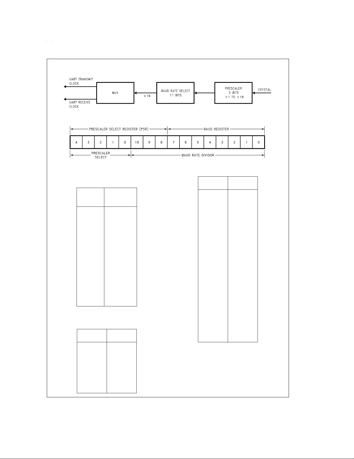
Baud Clock Generation (Continued)
FIGURE 14. USART BAUD Clock Generation
FIGURE 15. USART BAUD Clock Divisor Registers
DS012829-16
DS012829-17
TABLE 3. Baud Rate Divisors
(1.8432 MHz Prescaler Output)
Baud Baud Rate
Rate Divisor − 1
(N-1)
110
1046
(110.03)
134.5
855
(134.58)
150 767
300 383
600 191
1200 95
1800 63
2400 47
3600 31
4800 23
7200 15
9600 11
19200 5
38400 2
Note: The entries in
asynchronous mode the baud rate could be as high as 625k.
Table4
assume a prescaler outputof 1.8432 MHz. In the
TABLE 4. Prescaler Factors
Prescaler Prescaler
Select Factor
00000 NO CLOCK
00001 1
00010 1.5
00011 2
00100 2.5
00101 3
00110 3.5
00111 4
Prescaler Prescaler
Select Factor
01000 4.5
01001 5
01010 5.5
01011 6
01100 6.5
01101 7
01110 7.5
01111 8
10000 8.5
10001 9
10010 9.5
10011 10
10100 10.5
10101 11
10110 11.5
10111 12
11000 12.5
11001 13
11010 13.5
11011 14
11100 14.5
11101 15
11110 15.5
11111 16
www.national.com29
Page 30

Baud Clock Generation (Continued)
As an example, considering Asynchronous Mode and a CKI
clock of 4.608 MHz, the prescaler factor selected is:
4.608/1.8432 = 2.5
The 2.5 entry is available in
caler output is then used with proper Baud Rate Divisor
(
Table 3
) to obtain different baud rates. For a baud rate of
19200 e.g., the entry in
N−1=5(N−1isthevalue from
N=6(NistheBaud Rate Divisor)
Baud Rate = 1.8432 MHz/(16 x 6) = 19200
The divide by 16 is performed because in the asynchronous
mode, the input frequency to the USART is 16 times the
baud rate. The equation to calculate baud rates is given below.
The actual Baud Rate may be found from:
Where:
BR is the Baud Rate
Fc is the CKI frequency
N is the Baud Rate Divisor (
P is the Prescaler Divide Factor selected by the value in the
Prescaler Select Register (
Note: In the Synchronous Mode, the divisor 16 is replaced by two.
Example:
Asynchronous Mode:
Crystal Frequency=5MHz
Desired baud rate = 9600
Using the above equationNxPcanbecalculated first.
NxP=(5x10
Now 32.552 is divided by each Prescaler Factor (
obtain a value closest to an integer. This factor happens to
be 6.5 (P = 6.5).
N = 32.552/6.5 = 5.008 (N = 5)
The programmed value (from
Using the above values calculated for N and P:
BR=(5x10
%
error = (9615.385 − 9600)/9600 x 100 = 0.16
Table 4
. The 1.8432 MHz pres-
Table 3
is 5.
Table 3
BR = Fc/(16xNxP)
Table 3
).
Table 4
)
6
)/(16 x 9600) = 32.552
Table 3
) should be 4 (N − 1).
6
)/(16x5x6.5) = 9615.384
)
Table4
%
)to
Effect of HALT/IDLE
The USART logic is reinitialized when either the HALT or
IDLE modes are entered. This reinitialization sets the TBMT
flag and resets all read only bits in the USART control and
status registers. Read/Write bits remain unchanged. The
Transmit Buffer (TBUF) is not affected,but theTransmit Shift
register (TSFT) bits are set to one. The receiver registers
RBUF and RSFT are not affected.
The device will exit from the HALT/IDLE modes when the
Start bit of a character is detected at the RDX (L3) pin. This
feature is obtained by using the Multi-Input Wakeup scheme
provided on the device.
Before entering the HALT or IDLE modes the user program
must select the Wakeup source to be on the RDX pin. This
selection is done by setting bit 3 of WKEN (Wakeup Enable)
register.The Wakeup trigger condition is then selected to be
high to low transition. This is done via the WKEDG register
(Bit 3 is one.)
If the device is halted and crystal oscillator is used, the
Wakeup signal will notstart the chip running immediately be-
cause ofthe finite start up time requirement of the crystal oscillator.The idle timer (T0) generates a fixed (256 t
ensure that the oscillator has indeed stabilized before allowing the device to execute code. The user has to consider this
delay when data transfer is expected immediately after exiting the HALT mode.
) delayto
c
Diagnostic
Bits CHARL0 and CHARL1 in the ENU register provide a
loopback feature for diagnostic testing of the USART. When
these bits are setto one,the following occur: The receiver input pin (RDX) is internally connected to the transmitter output pin (TDX); the output of the Transmitter Shift Register is
“looped back” into the Receive Shift Register input. In this
mode, data that is transmitted is immediately received. This
feature allows the processor to verify the transmit and receive data paths of the USART.
Note that the framing format for this mode is the nine bit format; one Start bit, nine data bits, and 7/8, one or two Stop
bits. Parity is not generated or verified in this mode.
Attention Mode
The USARTReceiver section supports an alternate mode of
operation, referred to as ATTENTION Mode. This mode of
operation is selected by the ATTN bit in the ENUR register.
The data format for transmission must also be selected as
having nine Data bits and either 7/8, one or two Stop bits.
The ATTENTION mode of operation is intended for use in
networking the device with other processors. Typically in
such environments the messages consists of device addresses, indicating which of several destinations should receive them, and the actual data. This Mode supports a
scheme in which addresses are flagged by having the ninth
bit of the data field set to a 1. If the ninth bit is reset to a zero
the byte is a Data byte.
While in ATTENTION mode, the USART monitors the communication flow, but ignores all characters until an address
character is received. Upon receiving an address character,
the USART signals that the character is ready by setting the
RBFL flag, which in turn interrupts the processor if USART
Receiver interrupts are enabled. TheATTNbit isalso cleared
automatically at this point, so that data characters as well as
address characters are recognized. Software examines the
contents ofthe RBUF andresponds by deciding either to accept the subsequent datastream (byleaving theATTNbit reset) or to wait until the next address character is seen (by
setting the ATTN bit again).
Operation of the USARTTransmitter is not affectedby selection of this Mode. The value of the ninth bit to be transmitted
is programmed by setting XBIT9 appropriately. The value of
the ninth bit received is obtained by reading RBIT9. Since
this bit is located in ENUR register where the error flags reside, a bit operation on it will reset the error flags.
Comparators
The device contains two differential comparators, each with
a pair of inputs (positive and negative) and an output. Ports
I1–I3 and I4–I6 are used for the comparators. The following
is the Port I assignment:
I6 Comparator2 output
I5 Comparator2 positive input
I4 Comparator2 negative input
I3 Comparator1 output
www.national.com 30
Page 31
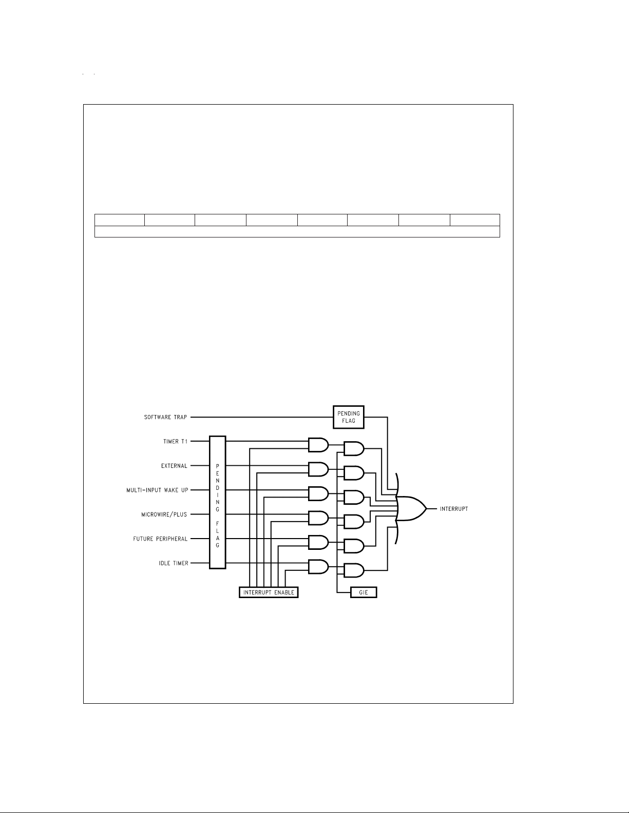
Comparators (Continued)
I2 Comparator1 positive input
I1 Comparator1 negative input
Only Comparator 1 is available on the CS series.
A Comparator Select Register (CMPSL) is used to enable
the comparators, read the outputs of the comparators internally, and enable the outputs of the comparators to the pins.
bit are associated with each comparator. Thecomparator result bits (CMP1RD and CMP2RD) are read only bits which
will readas zero if the associated comparator is not enabled.
The ComparatorSelect Register is cleared with reset, resulting in the comparators being disabled. The comparators
should also be disabled before entering either the HALT or
IDLE modes in order to save power. The configuration of the
CMPSL register is as follows:
Two control bits (enable and output enable) and one result
CMPSL REGISTER (ADDRESS X’00B7)
Reserved CMP20E CMP2RD CMP2EN CMP10E CMP1RD CMP1EN Reserved
Bit 7 Bit 0
The CMPSL register contains the following bits:
Reserved These bits are reserved and must be zero
CMP20E Selects pin I6 as comparator 2 output provided
that CMP2EN is set to enable the comparator
CMP2RD Comparator 2 result (this is a read only bit, which
will read as 0 if the comparator is not enabled)
CMP2EN Enable comparator 2
CMP10E Selects pin I3 as comparator 1 output provided
that CMPIEN is set to enable the comparator
CMP1RD Comparator 1 result (this is a read only bit, which
will read as 0 if the comparator is not enabled)
CMP1EN Enable comparator 1
Note: For compatibility with existing code and with existing Mask ROMMed
devices the bits of the CMPSL register will take precedence over the
associated Port F configuration and data output bits.
Interrupts
INTRODUCTION
Each device supports thirteen vectored interrupts. Interrupt
sources include Timer 0, Timer 1, Timer 2, Timer 3, Port L
Wakeup, Software Trap, MICROWIRE/PLUS, and External
Input.
All interruptsforce a branchto location 00FFHex in program
memory. The VIS instruction may be used to vector to the
appropriate service routine from location 00FF Hex.
The Software trap has the highest priority while the default
VIS has the lowest priority.
Each of the 13 maskable inputs has a fixed arbitration ranking and vector.
Figure 16
shows the Interrupt Block Diagram.
FIGURE 16. Interrupt Block Diagram
DS012829-28
www.national.com31
Page 32

Interrupts (Continued)
MASKABLE INTERRUPTS
All interrupts other than the Software Trap are maskable.
Each maskable interrupt has an associated enable bit and
pending flag bit. The pending bit is setto 1when theinterrupt
condition occurs. The state of the interrupt enable bit, combined with the GIE bit determineswhether an active pending
flag actually triggers an interrupt. All of the maskable interrupt pending and enable bits are contained in mapped control registers, and thus can be controlled by the software.
Amaskable interrupt condition triggers an interrupt underthe
following conditions:
1. The enable bit associated with that interrupt is set.
2. The GIE bit is set.
3. The device is not processing a non-maskable interrupt.
(If a non-maskable interrupt is being serviced, a
maskable interrupt must wait until that service routine is
completed.)
An interruptis triggered onlywhen all ofthese conditions are
met at the beginning of an instruction. If different maskable
interrupts meet these conditions simultaneously, the highest
priority interrupt will be serviced first, and the other pending
interrupts must wait.
Upon Reset, all pending bits, individual enable bits, and the
GIE bit are reset to zero. Thus, a maskable interrupt condition cannot trigger an interrupt until the program enables itby
setting both the GIE bit and the individual enable bit. When
enabling an interrupt, the user should consider whether or
not a previously activated (set) pending bit should be acknowledged. If, at the time an interrupt is enabled, any previous occurrences of the interrupt should be ignored, the associated pending bit must be reset to zero prior to enabling
the interrupt. Otherwise, the interrupt may be simply enabled; ifthe pending bit is already set, it will immediately trigger an interrupt. A maskable interrupt is active if its associated enable and pending bits are set.
An interrupt is an asychronous event which may occur before, during, or after an instruction cycle.Any interrupt which
occurs during the execution of an instruction is not acknowledged until the start of thenext normallyexecuted instruction
is tobe skipped, theskip is performedbefore the pendinginterrupt is acknowledged.
At the start of interrupt acknowledgment, the following actions occur:
1. The GIEbit isautomatically resetto zero,preventing any
subsequent maskableinterrupt from interrupting the current service routine. Thisfeature prevents one maskable
interrupt from interrupting another one being serviced.
2. The address of the instruction about to be executed is
pushed onto the stack.
3. The program counter (PC) is loaded with 00FF Hex,
causing a jump to that program memory location.
The device requires seven instruction cycles to perform the
actions listed above.
If the user wishes to allow nested interrupts, the interrupts
service routine may setthe GIEbit to 1 by writing to thePSW
register,and thus allow other maskable interrupts tointerrupt
the current service routine. If nested interrupts are allowed,
caution must be exercised. The user must write the program
in such a way as to prevent stack overflow, loss of saved
context information, and other unwanted conditions.
The interrupt service routine stored at location 00FF Hex
should use the VIS instruction to determine the cause of the
interrupt, and jump to the interrupt handling routine corresponding to the highest priority enabled and active interrupt.
Alternately, the user may choose to poll all interrupt pending
and enable bits to determine the source(s) of the interrupt. If
more than one interrupt is active, the user’s program must
decide which interrupt to service.
Within a specific interrupt service routine, the associated
pending bit should be cleared. This is typically done as early
as possible in the service routine in order to avoid missing
the next occurrence of the same type of interrupt event.
Thus, if the same event occurs a second time, even while the
first occurrence is still being serviced, the second occurrence will be serviced immediately upon return from the current interrupt routine.
An interrupt service routine typically ends with an RETI instruction. This instruction setsthe GIE bit back to 1, pops the
address stored on thestack, andrestores that address to the
program counter.Program execution then proceeds with the
next instruction that would have been executed had there
been no interrupt. If there are any valid interrupts pending,
the highest-priority interrupt is serviced immediately uponreturn from the previous interrupt.
VIS INSTRUCTION
The general interrupt serviceroutine, which starts at address
00FF Hex, must be capable of handling all types of interrupts. The VIS instruction, together with an interrupt vector
table, directs the device to thespecific interrupthandling routine based on the cause of the interrupt.
VIS is a single-byte instruction, typically used at the very beginning of the general interrupt service routine at address
00FF Hex, or shortly after that point, just after the code used
for context switching. The VIS instruction determines which
enabled and pending interrupt has the highest priority, and
causes anindirect jump to the address corresponding to that
interrupt source. The jump addresses (vectors) for all possible interrupts sources are stored in a vector table.
The vector table may be aslong as32 bytes(maximum of16
vectors) andresides at the top of the 256-byte block containing the VIS instruction. However, if the VIS instruction is at
the very top of a 256-byte block (such as at 00FF Hex), the
vector table resides at the top of the next 256-byte block.
Thus, if the VIS instruction is located somewhere between
00FF and 01DF Hex (the usual case), the vector table is located between addresses 01E0 and 01FF Hex. If the VIS instruction is located between 01FF and 02DF Hex, then the
vector table is located between addresses 02E0 and 02FF
Hex, and so on.
Each vector is 15 bits long and points to the beginning of a
specific interrupt service routine somewhere in the 32 kbyte
memory space. Each vectoroccupies twobytes of the vector
table, with the higher-order byte at the lower address. The
vectors are arranged in order of interrupt priority. The vector
of the maskable interrupt with the lowest rank is located to
0yE0 (higher-order byte) and 0yE1 (lower-order byte). The
next priority interrupt is located at 0yE2 and 0yE3, and so
forth in increasing rank. The Software Trap has the highest
rank and its vector is always located at 0yFE and 0yFF. The
number of interrupts which can become active defines the
size of the table.
Table5
shows the types of interrupts, the interrupt arbitration
ranking, and the locations of the corresponding vectors in
the vector table.
The vector table shouldbe filled by the user with thememory
locations of the specific interrupt service routines. For ex-
www.national.com 32
Page 33
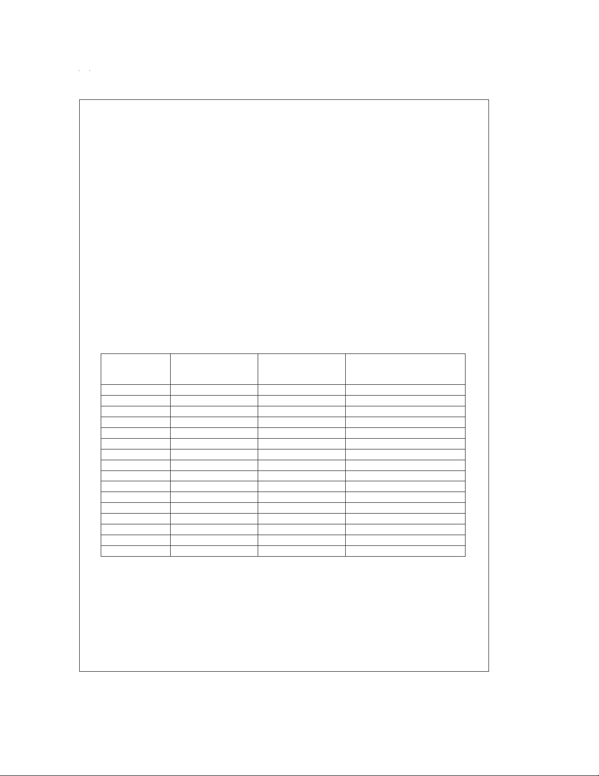
Interrupts (Continued)
ample, if the Software Trap routine is located at 0310 Hex,
then the vector location 0yFE and -0yFF should contain the
data 03 and 10 Hex, respectively. When a Software Trap interrupt occurs and the VIS instruction is executed, the program jumps to the address specified in the vector table.
The interrupt sources in the vector table are listed in order of
rank, from highest to lowest priority. If two or more enabled
and pending interrupts are detected at the same time, the
one with the highest priority is serviced first. Upon return
from the interrupt service routine, the next highest-level
pending interrupt is serviced.
If the VIS instruction is executed, but no interrupts are enabled and pending, the lowest-priority interrupt vector is
used, and a jump is made to the corresponding address in
the vector table. This is an unusual occurrence, and may be
the result of an error. It can legitimately result from a change
in the enable bits or pending flags prior to the execution of
the VIS instruction, such as executing a single cycle instruction which clears an enable flag at the same time that the
pending flag is set.It can also result, however, frominadvertent execution of the VIS command outside of the context of
an interrupt.
The default VIS interrupt vector can be useful for applications in which time critical interrupts can occur during the
gram context (A, B, X, etc.) and executing the RETI instruction, an interrupt service routine can beterminated by returning to the VIS instruction. In this case, interrupts will be
serviced in turn until no further interrupts are pending and
the default VIS routine is started. After testing the GIE bit to
ensure that execution is not erroneous, the routine should
restore the program context and execute the RETI to return
to the interrupted program.
This technique can save up to fifty instruction cycles (t
more, (50µs at 10 MHz oscillator) of latency for pending in-
), or
c
terrupts with a penalty of fewer than ten instruction cycles if
no further interrupts are pending.
To ensure reliable operation, the user should always use the
VIS instruction to determine the source of an interrupt. Although it is possible to poll the pending bits to detect the
source of an interrupt, this practiceis notrecommended. The
use of polling allowsthe standardarbitration ranking to be altered, but the reliability of the interrupt system is compromised. The polling routine must individually test the enable
and pending bits of each maskable interrupt. If a Software
Trap interrupt should occur, it will be serviced last, even
though it should have the highest priority. Under certain conditions, a Software Trapcould be triggered but not serviced,
resulting in an inadvertent “locking out” of all maskable interrupts by the Software Trap pending flag. Problems such as
this can be avoided by using VIS instruction.
servicing of another interrupt. Rather than restoring the pro-
TABLE 5. Interrupt Vector Table
Arbitration
Ranking
Source Description
Vector Address (Note *NO
TARGET FOR FNXref NS7955*)
(Hi-Low Byte)
(1) Highest Software INTR Instruction 0yFE–0yFF
(2) Reserved 0yFC–0yFD
(3) External G0 0yFA–0yFB
(4) Timer T0 Underflow 0yF8–0yF9
(5) Timer T1 T1A/Underflow 0yF6–0yF7
(6) Timer T1 T1B 0yF4–0yF5
(7) MICROWIRE/PLUS BUSY Low 0yF2–0yF3
(8) Reserved 0yF0–0yF1
(9) UART Receive 0yEE–0yEF
(10) UART Transmit 0yEC–0yED
(11) Timer T2 * T2A/Underflow 0yEA–0yEB
(12) Timer T2 * T2B 0yE8–0yE9
(13) Timer T3 * T2A/Underflow 0yE6–0yE7
(14) Timer T3 * T3B 0yE4–0yE5
(15) Port L/Wakeup Port L Edge 0yE2–0yE3
(16) Lowest Default VIS Reserved 0yE0–0yE1
Note 13: y is a variablewhich represents the VIS block. VIS and the vector table must be locatedin the same 256-byte block except if VIS is located at the lastaddress of a block. In this case, the table must be in the next block.
*
Reserved on the CS series.
www.national.com33
Page 34
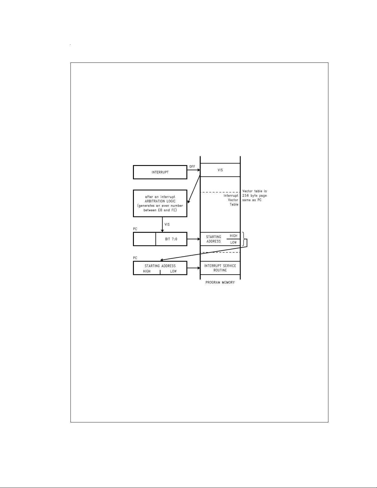
Interrupts (Continued)
VIS Execution
When the VIS instruction is executed it activates the arbitration logic. The arbitration logic generates an even number
between E0 and FE (E0, E2, E4, E6 etc...) depending on
which active interrupt has the highest arbitration ranking at
the time of the 1st cycle of VIS is executed. For example, if
the software trap interrupt is active, FE is generated. If the
external interrupt is active and the software trap interrupt is
not, then FAis generated and soforth. Ifthe only active interrupt is software trap, than E0 is generated. This number replaces the lower byteof thePC. Theupper byte of the PC remains unchanged. The new PC is therefore pointing to the
vector of the active interrupt with thehighest arbitration rank-
ing. This vector is read from program memory and placed
into the PC which is now pointed to the 1st instruction of the
service routineof the active interrupt with the highest arbitration ranking.
Figure 17
instruction.
tion.
The non-maskable interrupt pending flag is cleared by the
RPND (Reset Non-Maskable Pending Bit) instruction (under
certain conditions) and upon RESET.
illustrates the different steps performed by the VIS
Figure 18
shows a flowchart for the VIS instruc-
FIGURE 17. VIS Operation
www.national.com 34
DS012829-29
Page 35
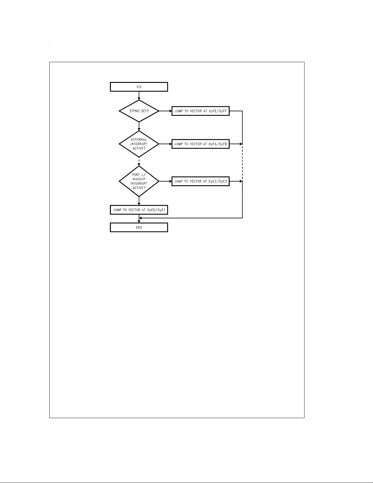
Interrupts (Continued)
DS012829-30
FIGURE 18. VIS Flowchart
www.national.com35
Page 36

Interrupts (Continued)
Programming Example: External Interrupt
PSW =00EF
CNTRL =00EE
RBIT 0,PORTGC
RBIT 0,PORTGD ; G0 pin configured Hi-Z
SBIT IEDG, CNTRL ; Ext interrupt polarity; falling edge
SBIT EXEN, PSW ; Enable the external interrupt
WAIT: JP WAIT ; Wait for external interrupt
INT_EXIT:
SERVICE: RBIT EXPND, PSW ; Interrupt Service Routine
SBIT GIE, PSW ; Set the GIE bit
.
.
.
.=0FF ; The interrupt causes a
VIS ; branch to address 0FF
; The VIS causes a branch to
;interrupt vector table
.
.
.
.=01FA ; Vector table (within 256 byte
.ADDRW SERVICE ; of VIS inst.) containing the ext
; interrupt service routine
.
.
RETI
.
.
; Reset ext interrupt pend. bit
.
.
.
JP INT_EXIT ; Return, set the GIE bit
www.national.com 36
Page 37

Interrupts (Continued)
NON-MASKABLE INTERRUPT
Pending Flag
There is a pending flag bit associatedwith the non-maskable
interrupt, called STPND. This pending flag is not memorymapped and cannot be accessed directly by the software.
The pending flag is reset to zero when a device Reset occurs. When the non-maskable interrupt occurs, the associated pending bit is set to 1. The interrupt service routine
should containan RPND instruction to reset the pending flag
to zero. The RPND instruction always resets the STPND
flag.
Software Trap
The Software Trap is a special kind of non-maskable interrupt which occurs when the INTR instruction (used to acknowledge interrupts) is fetched from program memory and
placed in the instruction register. This can happen in a variety of ways, usually because of an error condition. Some examples of causes are listed below.
If the program counter incorrectly points to a memory location beyond the available program memory space, the nonexistent or unused memory location returns zeroes which is
interpreted as the INTR instruction.
If the stack is popped beyond the allowed limit (address 06F
Hex), a 7FFF will be loaded intothe PC, if this lastlocation in
program memory is unprogrammed or unavailable, a Software Trap will be triggered.
A Software Trap can be triggered by a temporary hardware
condition such as a brownout or power supply glitch.
The Software Trap has the highest priority of all interrupts.
When a Software Trap occurs, the STPND bit is set. The GIE
bit is not affected and the pending bit (not accessible by the
user) is used to inhibit other interrupts and to direct the program tothe ST service routine withthe VIS instruction. Nothing can interrupt a Software Trap service routine except for
another SoftwareTrap. TheSTPND can be reset only by the
RPND instruction or a chip Reset.
The Software Trap indicates an unusual or unknown error
condition. Generally, returning to normal execution at the
point where the Software Trap occurred cannot be done reliably. Therefore, the Software Trap service routine should
reinitialize the stack pointer and perform a recovery procedure that restarts the software at some known point, similar
to a device Reset, but not necessarily performing all the
same functionsas a deviceReset. The routine must also execute the RPND instruction to reset the STPND flag. Otherwise, all other interruptswill be locked out. To the extent possible, the interrupt routine should record or indicate the
context of the device so that the cause of the Software Trap
can be determined.
If the user wishes to return to normal execution from the
point at which the Software Trap was triggered, the user
must first execute RPND, followed by RETSK rather than
RETI or RET. This is because the return address stored on
the stack is theaddress of the INTR instructionthat triggered
the interrupt. The program must skip that instruction in order
to proceed with the next one. Otherwise, an infinite loop of
Software Traps and returns will occur.
Programming a return to normal execution requires careful
consideration. If the Software Trap routine is interrupted by
another Software Trap, the RPND instruction in the service
routine for the second Software Trap will reset the STPND
flag; upon return to the first Software Trap routine, the
STPND flag will have the wrong state. This will allow
maskable interrupts to beacknowledged duringthe servicing
of the first Software Trap.Toavoid problems such as this, the
user program should contain the Software Trap routine to
perform a recovery procedure rather than a return to normal
execution.
Under normal conditions, the STPND flag is reset by a
RPND instruction in the Software Trap service routine. If a
programming error or hardware condition (brownout, power
supply glitch, etc.) sets the STPND flag without providing a
way for it to be cleared, all other interrupts will be locked out.
To alleviate this condition, the user can use extra RPND instructions in the main program and in the WATCHDOG service routine (if present). There is no harm in executing extra
RPND instructions in these parts of the program.
PORT L INTERRUPTS
Port L provides the user with an additional eight fully selectable, edgesensitive interrupts which are all vectored into the
same service subroutine.
The interrupt from Port L shares logic with the wake up circuitry.The register WKEN allows interrupts from Port L to be
individually enabledor disabled. The register WKEDGspecifies the trigger condition to be either a positive or a negative
edge. Finally, the register WKPND latches in the pending
trigger conditions.
The GIE (Global Interrupt Enable) bit enables the interrupt
function.
A control flag, LPEN, functions as a global interrupt enable
for Port L interrupts. Setting the LPEN flag will enable interrupts and vice versa. A separate global pending flag is not
needed since the register WKPND is adequate.
Since Port L is also used for waking the device out of the
HALTor IDLE modes, the user can elect to exit the HALT or
IDLE modes either withor without the interrupt enabled.If he
elects to disable the interrupt, then the device will restart execution from the instruction immediately following the instruction that placed the microcontroller in the HALT or IDLE
modes. In the other case, the device will first execute the interrupt service routine and then revert to normal operation.
(See HALT MODE for clock option wakeup information.)
INTERRUPT SUMMARY
The device uses the following types of interrupts, listed below in order of priority:
1. The Software Trap non-maskable interrupt, triggered by
the INTR (00 opcode) instruction. The Software Trap is
acknowledged immediately. This interrupt service routine can be interrupted only by another Software Trap.
The Software Trap should end with two RPND instructions followed by a restart procedure.
2. Maskable interrupts, triggered by an on-chip peripheral
block or an external device connected to the device. Under ordinary conditions, a maskable interrupt will not interrupt any other interrupt routine in progress. A
maskable interrupt routine in progress can be interrupted by the non-maskable interrupt request. A
maskable interrupt routine should end with an RETI instruction or, prior to restoring context, should return to
execute the VIS instruction. This is particularly useful
when exiting long interrupt service routiness if the time
between interrupts is short. In thiscase theRETI instruction would only be executed when the default VIS routine is reached.
www.national.com37
Page 38
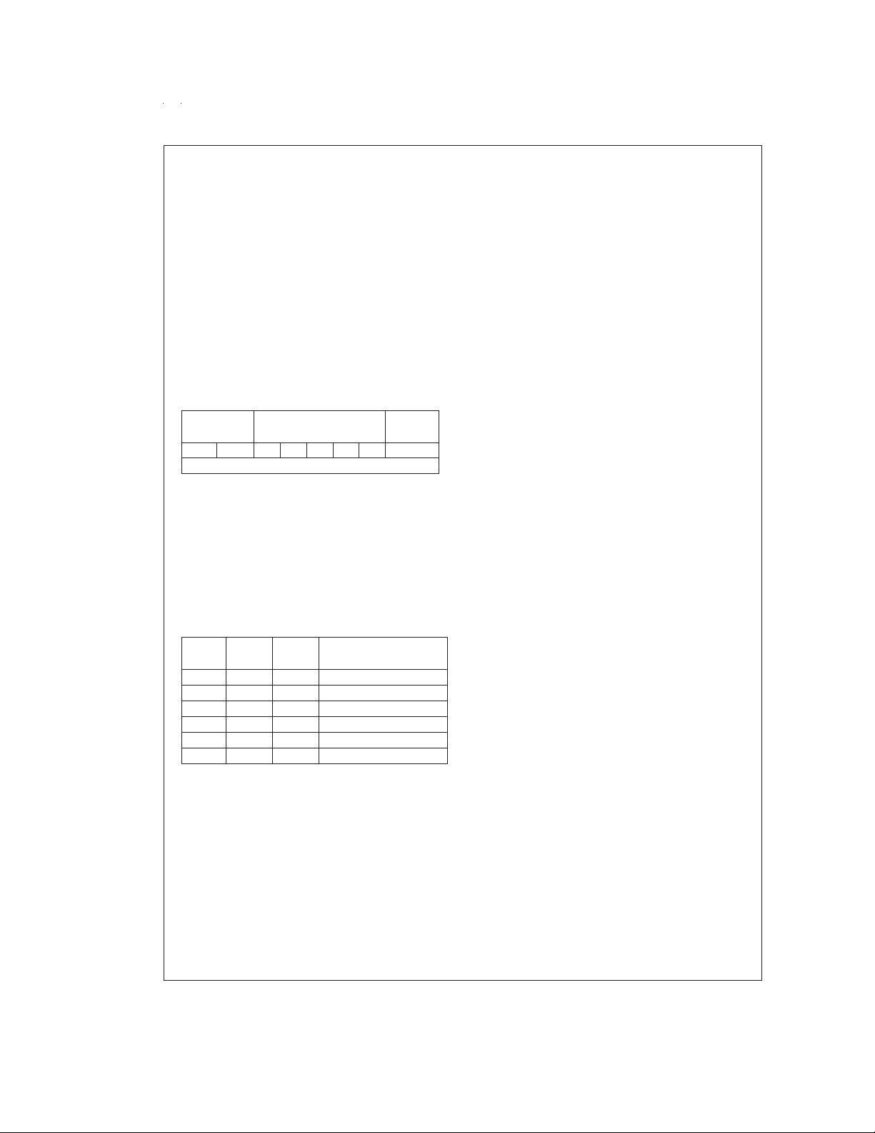
WATCHDOG
The device contains a WATCHDOG and clock monitor. The
WATCHDOG is designed to detect the user program getting
stuck in infinite loops resulting in loss of program control or
“runaway” programs. The ClockMonitor is used to detect the
absence of a clock or a very slow clock below a specified
rate on the CKI pin.
The WATCHDOG consists of two independent logic blocks:
WD UPPER and WD LOWER. WD UPPER establishes the
upper limit on the service window and WD LOWER defines
the lower limit of the service window.
Servicing the WATCHDOG consists of writing a specific
value to a WATCHDOG Service Register named WDSVR
which is memory mapped in the RAM. This value is composed of three fields, consisting of a 2-bit Window Select, a
5-bit Key Data field, and the 1-bit Clock Monitor Select field.
Table 6
shows the WDSVR register.
TABLE 6. WATCHDOG Service Register (WDSVR)
Window Key Data Clock
Select Monitor
X X 01100 Y
7 6 54321 0
The lowerlimit of the service window is fixed at 2048 instruction cycles. Bits 7 and 6 of the WDSVR register allow the
user to pick an upper limit of the service window.
Table 7
shows the four possible combinations of lower and
upper limits for the WATCHDOG service window. This flexibility in choosing the WATCHDOG service window prevents
any undue burden on the user software.
Bits 5, 4, 3, 2 and 1 of the WDSVR register represent the
5-bit Key Data field. The key data is fixed at 01100. Bit 0 of
the WDSVR Register is the Clock Monitor Select bit.
TABLE 7. WATCHDOG Service Window Select
WDSVR WDSVR Clock Service Window
Bit 7 Bit 6 Monitor (Lower-Upper Limits)
0 0 x 2048–8k t
0 1 x 2048–16k t
1 0 x 2048–32k t
1 1 x 2048–64k t
C
C
C
C
Cycles
Cycles
Cycles
Cycles
x x 0 Clock Monitor Disabled
x x 1 Clock Monitor Enabled
Clock Monitor
The Clock Monitor aboard the device can be selected or deselected under program control. The Clock Monitor is guaranteed not to reject the clock if the instruction cycle clock (1/
t
) is greater orequal to10 kHz.This equates to a clock input
c
rate on CKI of greater or equal to 100 kHz.
WATCHDOG Operation
The WATCHDOG and Clock Monitor are disabled during reset. The device comes out of reset with the WATCHDOG
armed, the WATCHDOG Window Select bits (bits 6, 7 of the
WDSVR Register) set, and the Clock Monitor bit (bit 0 of the
WDSVR Register) enabled. Thus, a Clock Monitor error will
occur after coming out of reset, if the instruction cycle clock
frequency has not reached a minimum specified value, including the case where the oscillator fails to start.
The WDSVR register can be written to only once after reset
and the key data (bits 5 through 1 of the WDSVR Register)
must matchto be a valid write.This write to the WDSVR register involves two irrevocable choices: (i) the selection of the
WATCHDOG service window (ii) enabling or disabling of the
Clock Monitor. Hence, the first write to WDSVR Register involves selecting or deselecting the Clock Monitor, select the
WATCHDOG service window and match the WATCHDOG
key data. Subsequent writes to the WDSVR register will
compare the value being written by the user to the WATCHDOG service window value and the key data (bits 7 through
1) in the WDSVR Register.
Table 8
shows the sequence of
events that can occur.
The user must service the WATCHDOG at least once before
the upper limit of the service window expires. The WATCHDOG may not be serviced more than once in every lower
limit of the service window. The user may service the
WATCHDOG as many timesas wishedin the time period between the lower and upper limits of the service window. The
first write to the WDSVR Register is also counted as a
WATCHDOG service.
The WATCHDOG has an output pin associated with it. This
is the WDOUT pin, on pin 1 of the port G. WDOUT is active
low.The WDOUTpin isin the high impedance statein the inactive state. Upon triggering the WATCHDOG, the logic will
pull the WDOUT (G1) pin low for an additional 16 t
cycles after the signal level on WDOUT pin goes below the
–32t
c
lower Schmitt trigger threshold. After this delay, the device
will stop forcing the WDOUT output low.
The WATCHDOG service window will restart when the WDOUT pin goes high. It is recommended that the user tie the
WDOUT pin back to V
WDOUT high.
through a resistor in order to pull
CC
AWATCHDOGservice whilethe WDOUTsignal is active will
be ignored. The state of the WDOUT pin is not guaranteed
on reset, but if it powers up low then the WATCHDOG will
time out and WDOUT will enter high impedance state.
The Clock Monitor forces the G1 pin low upon detecting a
clock frequency error. The Clock Monitor error will continue
until theclock frequency hasreached the minimumspecified
value, after which the G1 output will enter the high impedance TRI-STATE mode following 16 t
The ClockMonitor generates a continual Clock Monitor error
–32 tcclock cycles.
c
if the oscillator fails to start, or fails to reach the minimum
specified frequency. The specification for the Clock Monitor
is as follows:
>
1/t
10 kHz— No clock rejection.
c
<
10 Hz— Guaranteed clock rejection.
1/t
c
WATCHDOG AND CLOCK MONITOR SUMMARY
The following salient points regarding the WATCHDOG and
CLOCK MONITOR should be noted:
Both the WATCHDOG and CLOCK MONITOR detector
•
circuits are inhibited during RESET.
Following RESET, the WATCHDOG and CLOCK MONI-
•
TOR are both enabled, with the WATCHDOG having he
maximum service window selected.
The WATCHDOG service window and CLOCK MONI-
•
TOR enable/disable option can only be changed once,
during the initial WATCHDOG service following RESET.
c
www.national.com 38
Page 39
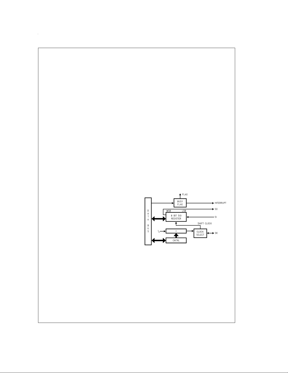
WATCHDOG Operation (Continued)
The initial WATCHDOG service must match the key data
•
value in the WATCHDOG Service register WDSVR in order to avoid a WATCHDOG error.
Subsequent WATCHDOG services must match all three
•
data fields in WDSVR in order to avoid WATCHDOG errors.
The correct key data value cannot be read from the
•
WATCHDOG Service register WDSVR. Any attempt to
read this key data value of 01100 from WDSVR will read
as key data value of all 0’s.
The WATCHDOG detector circuit is inhibited during both
•
the HALT and IDLE modes.
The CLOCK MONITOR detector circuit is active during
•
both the HALT and IDLE modes. Consequently, the device inadvertently entering the HALT mode will be detected as a CLOCK MONITOR error (provided that the
CLOCK MONITOR enable option has been selected by
the program).
With the single-pin R/C oscillator mask option selected
•
and the CLKDLY bit reset, the WATCHDOG service window will resume following HALT mode from where it left
off before entering the HALT mode.
With the crystal oscillator mask option selected, or with
•
the single-pin R/C oscillator mask option selected andthe
CLKDLYbit set, the WATCHDOG service window will be
set to its selected value from WDSVR following HALT.
Consequently, the WATCHDOG should not be serviced
for at least 2048 instruction cycles following HALT, but
must be serviced within the selected window to avoid a
WATCHDOG error.
The IDLE timer T0 is not initialized with RESET.
•
The user can sync in to the IDLE counter cycle with an
•
IDLE counter (T0) interrupt or by monitoring the T0PND
flag. The T0PND flag is set whenever the thirteenth bit of
the IDLE counter toggles (every 4096 instruction cycles).
The user is responsible for resetting the T0PND flag.
A hardware WATCHDOG service occurs just as the de-
•
vice exits the IDLE mode. Consequently, the WATCHDOG should not be serviced for at least 2048 instruction
cycles following IDLE, but must be serviced within theselected window to avoid a WATCHDOG error.
Following RESET, the initial WATCHDOGservice (where
•
the service window and the CLOCK MONITOR enable/
disable must be selected) may be programmed anywhere within the maximum service window (65,536 instruction cycles) initialized byRESET.Note thatthis initial
WATCHDOG service may be programmed within the initial 2048 instruction cycles without causing a WATCHDOG error.
Detection of Illegal Conditions
The device can detect various illegal conditions resulting
from coding errors, transient noise, power supply voltage
drops, runaway programs, etc.
Reading of undefined ROM gets zeros. The opcode for software interrupt is zero. If the program fetches instructions
from undefined ROM, this will force asoftware interrupt, thus
signaling that an illegal condition has occurred.
The subroutine stack grows down for each call (jump to subroutine), interrupt, or PUSH, and grows up for each return or
POP.The stack pointer is initialized to RAM location 06FHex
during reset. Consequently, if there are more returns than
calls, the stack pointer will point to addresses 070 and 071
Hex (which are undefined RAM). Undefined RAM from addresses 070 to 07F (Segment 0), and all other segments
(i.e., Segments 4 … etc.) is read as all 1’s, which in turn will
cause theprogram to return to address 7FFF Hex. This is an
undefined ROM location and the instruction fetched (all 0’s)
from this location will generate a software interrupt signaling
an illegal condition.
Thus, the chip can detect the following illegal conditions:
1. Executing from undefined ROM
2. Over “POP”ing the stack by having more returns than
calls.
When the software interrupt occurs, the user can re-initialize
the stack pointer and do arecovery procedurebefore restarting (this recovery program is probably similar to that following reset, but might not contain the same program initialization procedures). The recovery program should reset the
software interrupt pending bit using the RPND instruction.
MICROWIRE/PLUS
MICROWIRE/PLUS is a serial synchronous communications
interface. The MICROWIRE/PLUS capability enables the device to interface with any of National Semiconductor’s MICROWIRE peripherals (i.e. A/D converters, display drivers,
2
E
PROMs etc.) and with other microcontrollers which support the MICROWIRE interface. It consists of an 8-bit serial
shift register (SIO) with serial data input (SI), serial data output (SO) and serial shift clock (SK).
diagram of the MICROWIRE/PLUS logic.
FIGURE 19. MICROWIRE/PLUS Block Diagram
The shift clock canbe selectedfrom either an internal source
or an external source. Operating the MICROWIRE/PLUS arrangement withthe internal clock source is called the Master
mode of operation. Similarly, operating the MICROWIRE/
PLUS arrangement with an external shift clock is called the
Slave mode of operation.
The CNTRL register is used to configure and control the
MICROWIRE/PLUS mode. To use the MICROWIRE/PLUS,
the MSELbit in the CNTRL register is set to one. In the master mode, the SK clock rate is selected by the two bits, SL0
and SL1, in the CNTRL register.
clock rates that may be selected.
Figure 19
Table9
details the different
shows a block
DS012829-19
www.national.com39
Page 40
MICROWIRE/PLUS (Continued)
TABLE 8. WATCHDOG Service Actions
Key Window Clock Action
Data Data Monitor
Match Match Match Valid Service: Restart Service Window
Don’t Care Mismatch Don’t Care Error: Generate WATCHDOG Output
Mismatch Don’t Care Don’t Care Error: Generate WATCHDOG Output
Don’t Care Don’t Care Mismatch Error: Generate WATCHDOG Output
TABLE 9. MICROWIRE/PLUS
Master Mode Clock Select
SL1 SL0 SK
0 0 2xt
0 1 4xt
1 x 8xt
Where tcis the instruction cycle clock
MICROWIRE/PLUS OPERATION
Setting the BUSY bit in the PSW register causes the
MICROWIRE/PLUS to start shifting the data. It gets reset
when eight data bits have been shifted. The user may reset
the BUSY bit by software to allow less than 8 bits to shift. If
enabled, an interrupt is generated when eight data bits have
been shifted. The device may enter the MICROWIRE/PLUS
mode eitheras a Master or as a Slave.
Figure 20
two microcontroller devices and several peripherals may be
interconnected using the MICROWIRE/PLUSarrangements.
Warning:
The SIOregister should only be loaded when the SK clock is
low. Loading the SIO register while the SK clock is high will
result in undefined data in the SIO register. SK clock is normally low when not shifting.
Setting the BUSY flag when the input SK clock is high in the
MICROWIRE/PLUS slave mode may cause the current SK
clock for the SIO shift register to be narrow. For safety, the
BUSY flag should only be set whenthe input SK clock is low.
MICROWIRE/PLUS Master Mode Operation
In the MICROWIRE/PLUS Master mode of operation the
shift clock (SK) is generated internally by the device.The MICROWIRE Master always initiates all data exchanges. The
MSEL bit in the CNTRL register must be set to enable the
SO and SK functions onto the G Port. The SO and SK pins
must also be selected as outputs by setting appropriate bits
in the Port G configuration register.
Table10
bit settings required for Master mode of operation.
MICROWIRE/PLUS Slave Mode Operation
In the MICROWIRE/PLUS Slave mode of operation the SK
clock is generated by an external source. Setting the MSEL
bit in the CNTRL register enables the SO and SK functions
c
c
c
shows how
summarizes the
onto the G Port. The SK pin must be selected as an input
and the SO pinis selectedas an output pin by setting and resetting the appropriate bits in the Port G configuration register.
Table 10
summarizes the settings required to enter the
Slave mode of operation.
The user must set the BUSY flag immediately upon entering
the Slavemode. This will ensure that all data bits sent by the
Master will be shifted properly. After eight clock pulses the
BUSY flag will be cleared and the sequence may be repeated.
Alternate SK Phase Operation
The device allows either the normal SK clock or an alternate
phase SK clock to shift data in and out of the SIO register. In
both the modes the SK is normally low. In the normal mode
data is shifted in on the rising edge of the SK clock and the
data is shifted out on the falling edge of the SK clock. The
SIO register is shifted on each falling edge of the SK clock.
In the alternate SK phase operation, data is shifted in on the
falling edge of the SK clock and shifted out on the rising edge
of the SK clock.
A control flag, SKSEL, allows either the normal SK clock or
the alternate SK clock to be selected. Resetting SKSEL
causes the MICROWIRE/PLUS logic to be clocked from the
normal SK signal. Setting the SKSEL flag selects the alternate SK clock. The SKSEL is mapped into the G6 configuration bit. The SKSEL flag will power up in the reset condition,
selecting the normal SK signal.
TABLE 10. MICROWIRE/PLUS Mode Settings
This table assumes that the control flag MSEL is set.
G4 (SO) G5 (SK) G4 G5 Operation
Config. Bit Config. Bit Fun. Fun.
1 1 SO Int. MICROWIRE/PLUS
0 1 TRI- Int. MICROWIRE/PLUS
1 0 SO Ext. MICROWIRE/PLUS
0 0 TRI- Ext. MICROWIRE/PLUS
SK Master
STATE SK Master
SK Slave
STATE SK Slave
www.national.com 40
Page 41
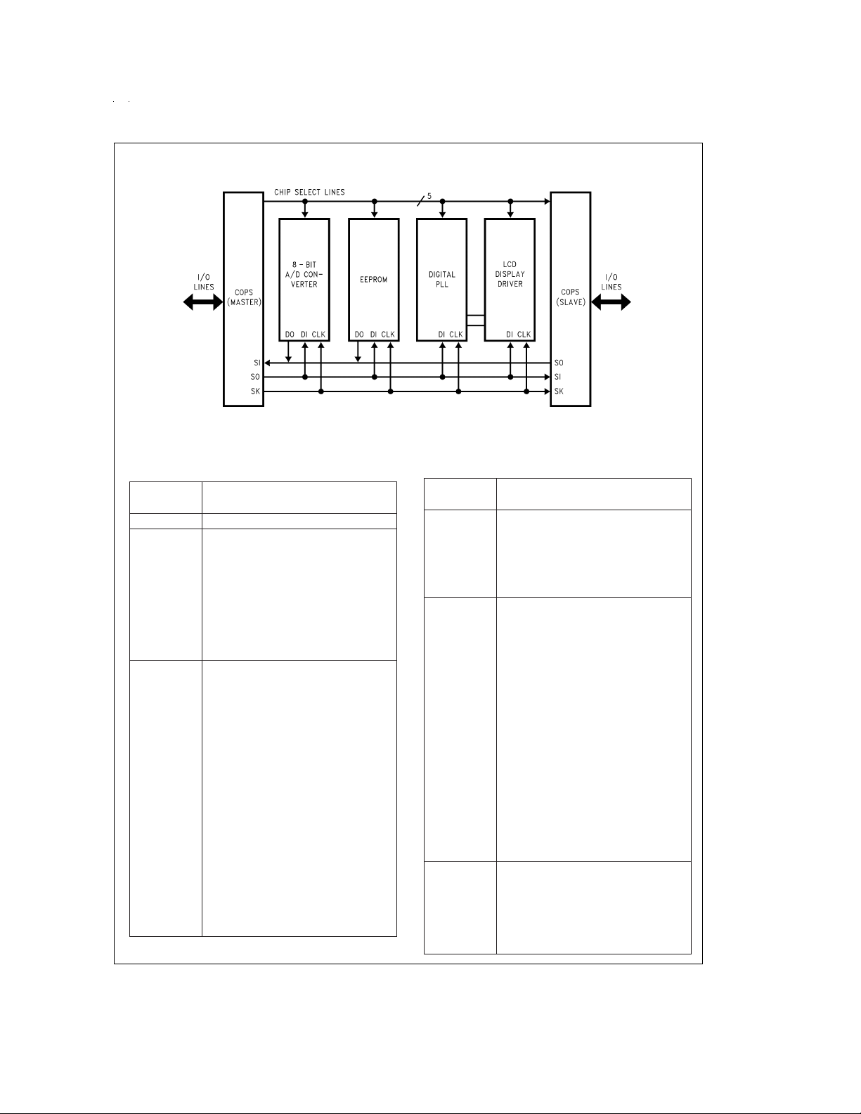
MICROWIRE/PLUS (Continued)
FIGURE 20. MICROWIRE/PLUS Application
Memory Map
All RAM, ports and registers (except A and PC) are mapped into data memory address space.
Address Contents
S/ADD REG
0000 to 006F On-Chip RAM bytes (112 bytes)
0070 to 007F Unused RAM Address Space (Reads As
All Ones)
xx80 to xx93 Unused RAM Address Space (Reads
Undefined Data)
xx94 Port F data register, PORTFD
xx95 Port F configuration register, PORTFC
xx96 Port F input pins (read only), PORTFP
xx97 to xxAF Unused address space (Reads
Undefined Data)
xxB0 Timer T3 Lower Byte
xxB1 Timer T3 Upper Byte
xxB2 Timer T3 Autoload Register T3RA Lower
Byte
xxB3 Timer T3 Autoload Register T3RA Upper
Byte
xxB4 Timer T3 Autoload Register T3RB Lower
Byte
xxB5 Timer T3 Autoload Register T3RB Upper
Byte
xxB6 Timer T3 Control Register
xxB7 Comparator Select Register
(Reg:CMPSL)
xxB8 UART Transmit Buffer (Reg:TBUF)
xxB9 UART Receive Buffer (Reg:RBUF)
xxBA UART Control and Status Register
(Reg:ENU)
xxBB UART Receive Control and Status
Register (Reg:ENUR)
Address Contents
S/ADD REG
xxBC UART Interrupt and Clock Source
Register (Reg:ENUI)
xxBD UART Baud Register (Reg:BAUD)
xxBE UART Prescale Select Register
(Reg:PSR)
xxBF Reserved for UART
xxC0 Timer T2 Lower Byte
xxC1 Timer T2 Upper Byte
xxC2 Timer T2 Autoload Register T2RA Lower
Byte
xxC3 Timer T2 Autoload Register T2RA Upper
Byte
xxC4 Timer T2 Autoload Register T2RB Lower
Byte
xxC5 Timer T2 Autoload Register T2RB Upper
Byte
xxC6 Timer T2 Control Register
xxC7 WATCHDOG Service Register
(Reg:WDSVR)
xxC8 MIWU Edge Select Register
(Reg:WKEDG)
xxC9 MIWU Enable Register (Reg:WKEN)
xxCA MIWU Pending Register (Reg:WKPND)
xxCB to xxCF Reserved
xxD0 Port L Data Register
xxD1 Port L Configuration Register
xxD2 Port L Input Pins (Read Only)
xxD3 Reserved for Port L
xxD4 Port G Data Register
xxD5 Port G Configuration Register
DS012829-20
www.national.com41
Page 42
Memory Map (Continued)
Address Contents
S/ADD REG
xxD6 Port G Input Pins (Read Only)
xxD7 Port I Input Pins (Read Only) (Actually
reads Port F input pins)
xxD8 Port C Data Register
xxD9 Port C Configuration Register
xxDA Port C Input Pins (Read Only)
xxDB Reserved for Port C
xxDC Port D
xxDD to xxDF Reserved for Port D
xxE0 to xxE5 Reserved for EE Control Registers
xxE6 Timer T1 Autoload Register T1RB Lower
Byte
xxE7 Timer T1 Autoload Register T1RB Upper
Byte
xxE8 ICNTRL Register
xxE9 MICROWIRE/PLUS Shift Register
xxEA Timer T1 Lower Byte
xxEB Timer T1 Upper Byte
Addressing Modes
There areten addressing modes, six for operand addressing
and four for transfer of control.
OPERAND ADDRESSING MODES
Register Indirect
This is the “normal” addressing mode. The operand is the
data memory addressed by the B pointer or X pointer.
Register Indirect (with auto post increment or
decrement of pointer)
This addressing mode is used with the LD and X instructions. The operand is the data memory addressed by the B
pointer or X pointer. This is a register indirect mode that automatically post increments or decrements the B or X register after executing the instruction.
Direct
The instruction contains an 8-bit address field that directly
points to the data memory for the operand.
Immediate
The instructioncontains an 8-bit immediate field as the operand.
Short Immediate
This addressingmode is usedwith the Load B Immediate instruction. The instruction contains a 4-bit immediate field as
the operand.
Indirect
This addressing mode is used with the LAID instruction. The
contents of the accumulator are used as a partial address
(lower 8 bits of PC) for accessing a data operand from the
program memory.
Address Contents
S/ADD REG
xxEC Timer T1 Autoload Register T1RA Lower
Byte
xxED Timer T1 Autoload Register T1RA Upper
Byte
xxEE CNTRL Control Register
xxEF PSW Register
xxF0 to FB On-Chip RAM Mapped as Registers
xxFC X Register
xxFD SP Register
xxFE B Register
xxFF S Register
0100–017F On-Chip 128 RAM Bytes
0200–027F On-Chip 128 RAM Bytes (Reads as
undefined data on COP8SGE)
0300–037F On-Chip 128 RAM Bytes (Reads as
undefined data on COP8SGE)
Note: Reading memory locations 0070H–007FH (Segment 0) will return all
ones. Reading unused memory locations 0080H–00AFH (Segment 0)
will return undefined data. Reading memory locations from other Segments (i.e., Segment 2, Segment 3, … etc.) will return undefined data.
TRANSFER OF CONTROL ADDRESSING MODES
Relative
This mode is used for the JP instruction, with the instruction
field being added to the program counter to get the new program location. JP has a range from −31 to +32 to allow a
1-byte relative jump (JP + 1 is implemented by a NOP instruction). There are no “pages” when using JP, since all 15
bits of PC are used.
Absolute
This mode is used with the JMP and JSR instructions, with
the instruction field of 12 bits replacing the lower 12 bits of
the program counter (PC). This allows jumping to any location in the current 4k program memory segment.
Absolute Long
This mode is usedwith the JMPL andJSRL instructions, with
the instruction field of 15 bits replacing the entire 15 bits of
the program counter (PC). This allows jumping to any location up to 32k in the program memory space.
Indirect
This mode is used with the JID instruction. The contents of
the accumulator are used as a partial address (lower 8 bits of
PC) for accessing a location in the program memory. The
contents of this program memory location serve as a partial
address (lower 8 bits of PC) for the jump to the next instruction.
Note: The VIS is a special caseof the Indirect Transferof Control addressing
mode, where the double byte vector associated with the interrupt is
transferred from adjacent addresses in the program memory into the
program counter (PC) in order to jump to the associated interrupt service routine.
www.national.com 42
Page 43

Instruction Set
Register and Symbol Definition
Registers
A 8-Bit Accumulator Register
B 8-Bit Address Register
X 8-Bit Address Register
S 8-Bit Segment Register
SP 8-Bit Stack Pointer Register
PC 15-Bit Program Counter Register
PU Upper 7 Bits of PC
PL Lower 8 Bits of PC
C 1 Bit of PSW Register for Carry
HC 1 Bit of PSW Register for Half Carry
GIE 1 Bit of PSW Register for Global Interrupt
VU Interrupt Vector Upper Byte
VL Interrupt Vector Lower Byte
[B] Memory Indirectly Addressed by B Register
[X] Memory Indirectly Addressed by X Register
MD Direct Addressed Memory
Mem Direct Addressed Memory or [B]
Meml Direct Addressed Memory or [B] or
Imm 8-Bit Immediate Data
Reg Register Memory: Addresses F0 to FF
Bit Bit Number (0 to 7)
←
↔
Enable
Symbols
Immediate Data
(Includes B, X and SP)
Loaded with
Exchanged with
www.national.com43
Page 44

Instruction Set (Continued)
INSTRUCTION SET
ADD A,Meml ADD A←A + Meml
ADC A,Meml ADD with Carry A←A+Meml+C,C←Carry
HC←Half Carry
SUBC A,Meml Subtract with Carry A←A−MemI+C,C←Carry
HC←Half Carry
AND A,Meml Logical AND A←A and Meml
ANDSZ A,Imm Logical AND Immed., Skip if Zero Skip next if (A and Imm)=0
OR A,Meml Logical OR A←A or Meml
XOR A,Meml Logical EXclusive OR A←A xor Meml
IFEQ MD,Imm IF EQual Compare MD and Imm, Do next if MD=Imm
IFEQ A,Meml IF EQual Compare A and Meml, Do next if A=Meml
IFNE A,Meml IF Not Equal Compare A and Meml, Do next if A
IFGT A,Meml IF Greater Than Compare A and Meml, Do next if A
IFBNE
DRSZ Reg Decrement Reg., Skip if Zero Reg←Reg − 1, Skip if Reg=0
SBIT
RBIT
IFBIT
RPND Reset PeNDing Flag Reset Software Interrupt Pending Flag
X A,Mem EXchange A with Memory A
X A,[X] EXchange A with Memory [X] A
LD A,Meml LoaD A with Memory A←Meml
LD A,[X] LoaD A with Memory [X] A←[X]
LD B,Imm LoaD B with Immed. B←Imm
LD Mem,Imm LoaD Memory Immed Mem←Imm
LD Reg,Imm LoaD Register Memory Immed. Reg←Imm
XA,[B
XA,[X
LD A, [B
LD A, [X
LD [B
CLR A CLeaR A A←0
INC A INCrement A A←A+1
DEC A DECrement A A←A−1
LAID Load A InDirect from ROM A←ROM (PU,A)
DCOR A Decimal CORrect A A←BCD correction of A (follows ADC, SUBC)
RRC A Rotate A Right thru C C→A7→…→A0→C
RLC A Rotate A Left thru C C←A7←…←A0←C
SWAP A SWAP nibbles of A A7…A4
SC Set C C←1, HC←1
RC Reset C C←0, HC←0
IFC IF C IF C is true, do next instruction
IFNC IF Not C If C is not true, do next instruction
POP A POP the stack into A SP←SP+1,A←[SP]
PUSH A PUSH A onto the stack [SP]←A, SP←SP−1
VIS Vector to Interrupt Service Routine PU←[VU], PL←[VL]
JMPL Addr. Jump absolute Long PC←ii (ii=15 bits, 0 to 32k)
JMP Addr. Jump absolute PC9…0←i(i=12 bits)
JP Disp. Jump relative short PC←PC+r(ris−31to+32, except 1)
#
#
,Mem Set BIT 1 to bit, Mem (bit=0 to 7 immediate)
#
,Mem Reset BIT 0 to bit, Mem
#
,Mem IF BIT If bit in A or Mem is true do next instruction
±
±
±
],Imm LoaD Memory [B] Immed. [B]←Imm, (B←B±1)
If B Not Equal Do next if lower 4 bits of B≠Imm
↔
Mem
↔
[X]
±
] EXchange A with Memory [B] A↔[B], (B←B±1)
±
] EXchange A with Memory [X] A↔[X], (X←X±1)
] LoaD A with Memory [B] A←[B], (B←B±1)
] LoaD A with Memory [X] A←[X], (X←X±1)
↔
A3…A0
≠
>
Meml
Meml
www.national.com 44
Page 45

Instruction Set (Continued)
INSTRUCTION SET (Continued)
JSRL Addr. Jump SubRoutine Long [SP]←PL, [SP−1]←PU,SP−2, PC←ii
JSR Addr Jump SubRoutine [SP]←PL, [SP−1]←PU,SP−2, PC9…0←i
JID Jump InDirect PL←ROM (PU,A)
RET RETurn from subroutine SP + 2, PL←[SP], PU←[SP−1]
RETSK RETurn and SKip SP + 2, PL←[SP],PU←[SP−1],
skip next instruction
RETI RETurn from Interrupt SP + 2, PL←[SP],PU←[SP−1],GIE←1
INTR Generate an Interrupt [SP]←PL, [SP−1]←PU, SP−2, PC←0FF
NOP No OPeration PC←PC+1
www.national.com45
Page 46
Instruction Execution Time
Most instructionsare single byte(with immediate addressing
mode instructions taking two bytes).
Most single byte instructions take one cycle time to execute.
Skipped instructions require x number of cycles to be
skipped, where x equals the number of bytes in the skipped
instruction opcode.
Bytes and Cycles per Instruction
The following table shows the number of bytes and cycles for
each instruction in the format of byte/cycle.
Arithmetic and Logic Instructions
[B] Direct Immed.
ADD 1/1 3/4 2/2
ADC 1/1 3/4 2/2
SUBC 1/1 3/4 2/2
AND 1/1 3/4 2/2
OR 1/1 3/4 2/2
XOR 1/1 3/4 2/2
IFEQ 1/1 3/4 2/2
IFNE 1/1 3/4 2/2
IFGT 1/1 3/4 2/2
IFBNE 1/1
DRSZ 1/3
SBIT 1/1 3/4
RBIT 1/1 3/4
IFBIT 1/1 3/4
RPND 1/1
Instructions Using A & C
CLRA 1/1
INCA 1/1
DECA 1/1
LAID 1/3
DCOR 1/1
RRCA 1/1
RLCA 1/1
SWAPA 1/1
SC 1/1
RC 1/1
IFC 1/1
IFNC 1/1
PUSHA 1/3
POPA 1/3
ANDSZ 2/2
Transfer of Control Instructions
JMPL 3/4
JMP 2/3
JP 1/3
JSRL 3/5
JSR 2/5
JID 1/3
VIS 1/5
RET 1/5
RETSK 1/5
RETI 1/5
INTR 1/7
NOP 1/1
Memory Transfer Instructions
Register Direct Immed. Register Indirect
Indirect Auto Incr. & Decr.
[B] [X] [B+, B−] [X+, X−]
X A, (Note 14) 1/1 1/3 2/3 1/2 1/3
LD A, (Note 14) 1/1 1/3 2/3 2/2 1/2 1/3
LD B, Imm 1/1 (IF B
LD B, Imm 2/2 (IF B
LD Mem, Imm 2/2 3/3 2/2
LD Reg, Imm 2/3
IFEQ MD, Imm 3/3
=
Note 14:
www.national.com 46
>
Memory location addressed by B or X or directly.
<
16)
>
15)
Page 47

Instruction Execution Time (Continued)
JP+23 JP+7 6
JP+22 JP+6 5
JP+21 JP+5 4
JP+20 JP+4 3
JP+17 INTR 0
JP+19 JP+3 2
JP+18 JP+2 1
Lower Nibble
JP+32 JP+16 F
JP+28 JP+12 B
JP+24 JP+8 7
JP+25 JP+9 8
JP+27 JP+11 A
JP+26 JP+10 9
JP+29 JP+13 C
JP+31 JP+15 E
JP+30 JP+14 D
Upper Nibble
JMP
x000–x0FF
x000–x0FF
IFBNE 0 JSR
LD
B,#0F
A, #i
ANDSZ
0,[B]
IFBIT
ADC
A,[B]
A,#i
RRCA RC ADC
JMP
JMP
x100–x1FF
x100–x1FF
IFBNE 2 JSR
IFBNE 1 JSR
B,#0E
*LD
*LD
1,[B]
IFBIT
IFBIT
A,[B]
IFEQ
SUBC
A, #i
IFEQ
X
* SC SUBC
X
JMP
x200–x2FF
x200–x2FF
IFBNE 3 JSR
B,#0D
*LD
2,[B]
IFBIT
A,[B]
IFGT
A,#i
IFGT
X
A,[B+]
X
A,[X+]
x300–x3FF
x300–x3FF
B,#0C
3,[B]
A,[B]
A,#i
A,[B−]
A,[X−]
JMP
x400–x4FF
x400–x4FF
IFBNE 4 JSR
B,#0B
CLRA LD
4,[B]
IFBIT
ADD
A,[B]
A,#i
VIS LAID ADD
JMP
IFBNE 5 JSR
SWAPA LD
IFBIT
AND
RPND JID AND
JMP
x500–x5FF
x500–x5FF
IFBNE 6 JSR
B,#0A
DCORA LD
5,[B]
IFBIT
XOR
A,[B]
A,#i
XOR
X A,[X] X
x600–x6FF
x600–x6FF
B,#09
6,[B]
A,[B]
A,#i
A,[B]
JMP
x700–x7FF
x700–x7FF
IFBNE 7 JSR
B,#08
PUSHA LD
7,[B]
IFBIT
A,[B]
* * OR A,#i OR
JMP
IFBNE 8 JSR
LD
RBIT
NOP RLCA LD A,#i IFC SBIT
x800–x8FF
x800–x8FF
B,#07
0,[B]
0,[B]
JMP
x900–x9FF
x900–x9FF
IFBNE 9 JSR
LD
B,#06
1,[B]
RBIT
1,[B]
IFNC SBIT
A,#i
IFNE
IFEQ
Md,#i
A,[B]
IFNE
JMP
IFBNE 0A JSR
LD
RBIT
INCA SBIT
LD
LD
LD
JMP
xA00–xAFF
xA00–xAFF
IFBNE 0B JSR
LD
B,#05
2,[B]
RBIT
2,[B]
DECA SBIT
LD
[B+],#i
LD
A,[B+]
LD
A,[X+]
JMP
xB00–xBFF
xB00–xBFF
IFBNE 0C JSR
LD
B,#04
3,[B]
RBIT
3,[B]
[B−],#i
JMPL X A,Md POPA SBIT
A,[B−]
LD
A,[X−]
xC00–xCFF
xC00–xCFF
B,#03
4,[B]
4,[B]
Md,#i
JMP
IFBNE 0D JSR
LD
RBIT
RETSK SBIT
DIR JSRL LD
xD00–xDFF
xD00–xDFF
B,#02
5,[B]
5,[B]
A,Md
JMP
IFBNE 0E JSR
LD
RBIT
RET SBIT
LD
LD
LD
xE00–xEFF
xE00–xEFF
B,#01
6,[B]
6,[B]
[B],#i
A,[B]
A,[X]
JMP
IFBNE 0F JSR
LD
RBIT
* * LD B,#i RETI SBIT
xF00–xFFF
xF00–xFFF
B,#00
7,[B]
7,[B]
Opcode Table
DRSZ
F E D C BA9 876 5 4 3 2 10
JP−15 JP−31 LD 0F0,
0F0
#i
0F1
DRSZ
#i
JP−14 JP−30 LD 0F1,
0F2
DRSZ
#i
JP−13 JP−29 LD 0F2,
0F3
DRSZ
#i
JP−12 JP−28 LD 0F3,
0F4
DRSZ
#i
JP−11 JP−27 LD 0F4,
0F5
DRSZ
#i
JP−10 JP−26 LD 0F5,
0F6
DRSZ
#i
JP−9 JP−25 LD 0F6,
0F7
DRSZ
#i
JP−8 JP−24 LD 0F7,
0F8
DRSZ
#i
JP−7 JP−23 LD 0F8,
0F9
DRSZ
#i
JP−6 JP−22 LD 0F9,
0FA
DRSZ
#i
JP−5 JP−21 LD 0FA,
0FB
DRSZ
#i
JP−4 JP−20 LD 0FB,
0FC
DRSZ
#i
JP−3 JP−19 LD 0FC,
0FD
DRSZ
#i
JP−2 JP−18 LD 0FD,
0FE
DRSZ
#i
JP−1 JP−17 LD 0FE,
0FF
DRSZ
#i
JP−0 JP−16 LD 0FF,
www.national.com47
i is the immediate data
Where,
Md is a directly addressed memory location
* is an unused opcode
The opcode 60 Hex is also the opcode for IFBIT #i,A
Page 48

Mask Options
The mask programmable options are shown below. The options are programmed at the same time as the ROM pattern
submission.
OPTION 1: CLOCK CONFIGURATION
=
1 Crystal Oscillator (CKI/10)
G7 (CKO) is clock generator output to crystal/
resonator with CKI being the clock input
=
2 Single-pin RC controlled oscillator (CKI/10)
G7 is available as a HALT restart and/or
general purpose input
OPTION 2: HALT
=
1 Enable HALT mode
=
2 Disable HALT mode
OPTION 3: BONDING OPTIONS
=
1 44-Pin PLCC
=
2 40-Pin DIP
=
3 N/A
=
4 28-DIP
=
5 28-Pin SO
Some device can be driven by a clock input on the CKI input
pin which can be between DC and 10 MHz. The CKO output
clock ison pin G7(if clock option=1 hasbeen selected). The
CKI input frequency is divided down by 10 to produce the instruction cycle clock (1/tc).
Not all packages are available for all devices, please check
order information.
Development Support
OVERVIEW
National isengaged with an international community of independent 3rd party vendors who provide hardware and software development tool support. Through National’s interaction and guidance, these tools cooperate to form a choice of
tools that fits each developer’s needs.
This section provides a summary of the tool and development kits currently available. Up-to-date information, selection guides, free tools, demos, updates, and purchase information can be obtained at our web site at:
www.national.com/cop8.
SUMMARY OF TOOLS
COP8 Evaluation Tools
COP8–NSEVAL: Free Software Evaluation package for
•
Windows. A fully integrated evaluation environment for
COP8, including versions of WCOP8 IDE (Integrated Development Environment), COP8-NSASM, COP8-MLSIM,
COP8C, DriveWay
information.
COP8–MLSIM: Free Instruction Level Simulator tool for
•
Windows. For testing and debugging software instructions only (No I/O or interrupt support).
COP8–EPU: Very Low cost COP8 Evaluation & Pro-
•
gramming Unit. Windows based evaluation and
hardware-simulation tool, with COP8 device programmer
and erasable samples. Includes COP8-NSDEV, Driveway COP8 Demo, MetaLink Debugger, I/O cables and
power supply.
™
COP8, Manuals, and other COP8
COP8–EVAL-ICUxx: Very Low cost evaluation and de-
•
sign test board for COP8ACC and COP8SGx Families,
from ICU. Real-time environment with add-on A/D, D/A,
and EEPROM. Includes software routines and reference
designs.
Manuals,Applications Notes,Literature: Available free
•
from our web site at: www.national.com/cop8.
COP8 Integrated Software/Hardware Design Development Kits
COP8-EPU: Very Low cost Evaluation & Programming
•
Unit. Windows based development and hardwaresimulation tool for COPSx/xG families, with COP8 device
programmer and samples. Includes COP8-NSDEV,
Driveway COP8 Demo, MetaLink Debugger, cables and
power supply.
COP8-DM: Moderatecost Debug Modulefrom MetaLink.
•
A Windows based, real-time in-circuit emulation tool with
COP8 device programmer. Includes COP8-NSDEV,
DriveWay COP8 Demo, MetaLink Debugger, power supply, emulation cables and adapters.
COP8 Development Languages and Environments
COP8-NSASM: Free COP8 Assembler v5 for Win32.
•
Macro assembler,linker, and librarian for COP8 software
development. Supports all COP8 devices. (DOS/Win16
v4.10.2 available with limited support). (Compatible with
WCOP8 IDE, COP8C, and DriveWay COP8).
COP8-NSDEV: Very low cost Software Development
•
Package for Windows. An integrated development environment for COP8, including WCOP8 IDE, COP8NSASM, COP8-MLSIM.
COP8C: Moderately priced C Cross-Compiler and Code
•
Development System from Byte Craft (no code limit). Includes BCLIDE (Byte Craft Limited Integrated Development Environment)for Win32, editor, optimizing C CrossCompiler, macro cross assembler, BC-Linker, and
MetaLink tools support. (DOS/SUN versions available;
Compiler is installable under WCOP8 IDE; Compatible
with DriveWay COP8).
EWCOP8-KS: Very Low cost ANSI C-Compiler and Em-
•
bedded Workbench from IAR (Kickstart version:
COP8Sx/Fx only with 2k code limit; No FP). A fully integrated Win32 IDE, ANSI C-Compiler, macro assembler,
editor, linker, Liberian, C-Spy simulator/debugger, PLUS
MetaLink EPU/DM emulator support.
EWCOP8-AS: Moderately priced COP8 Assembler and
•
Embedded Workbench from IAR (no code limit).Afully integrated Win32 IDE, macro assembler, editor, linker, librarian, and C-Spy high-level simulator/debugger with
I/O and interrupts support. (Upgradeable with optional
C-Compiler and/or MetaLink Debugger/Emulator support).
EWCOP8-BL: Moderately priced ANSI C-Compiler and
•
Embedded Workbench from IAR (Baseline version: All
COP8 devices; 4k code limit; no FP). A fully integrated
Win32 IDE, ANSI C-Compiler, macro assembler, editor,
linker,librarian, andC-Spy high-levelsimulator/debugger.
(Upgradeable; CWCOP8-MMetaLink tools interface support optional).
EWCOP8: Full featured ANSI C-Compiler and Embed-
•
ded Workbench for Windows from IAR (no code limit). A
fully integrated Win32 IDE, ANSI C-Compiler, macro assembler, editor, linker, librarian, and C-Spy high-level
simulator/debugger. (CWCOP8-M MetaLink tools interface support optional).
www.national.com 48
Page 49
Development Support (Continued)
EWCOP8-M: Full featured ANSI C-Compiler andEmbed-
•
ded Workbench for Windows from IAR (no code limit). A
fully integrated Win32 IDE, ANSI C-Compiler, macro assembler, editor, linker, librarian, C-Spy high-level
simulator/debugger, PLUS MetaLink debugger/hardware
interface (CWCOP8-M).
COP8 Productivity Enhancement Tools
WCOP8 IDE: Very Low cost IDE (Integrated Develop-
•
ment Environment) from KKD. Supports COP8C, COP8NSASM, COP8-MLSIM, DriveWay COP8, and MetaLink
debugger under a common Windows Project Management environment. Code development, debug, and emulation tools can be launched from the project window
framework.
DriveWay-COP8: Low cost COP8 Peripherals Code
•
Generation tool from Aisys Corporation. Automatically
generates tested and documented C orAssembly source
code modules containing I/O drivers and interrupt handlers for each on-chip peripheral. Application specific
code can be inserted for customization using the integrated editor. (Compatible with COP8-NSASM, COP8C,
and WCOP8 IDE.)
COP8-UTILS: Free set of COP8 assembly code ex-
•
amples, device drivers, and utilities to speed up code development.
COP8-MLSIM: Free Instruction Level Simulator tool for
•
Windows. For testing and debugging software instructions only (No I/O or interrupt support).
Vendor Tools Order Number Cost Notes
National COP8-NSEVAL COP8-NSEVAL Free Web site download
COP8-NSASM COP8-NSASM Free Included in EPU and DM. Web site download
COP8-MLSIM COP8-MLSIM Free Included in EPU and DM. Web site download
COP8-NSDEV COP8-NSDEV VL Included in EPU and DM. Order CD from website
COP8-EPU COP8SG-EPU (-1 or -2) VL -1 = 110V, -2 = 220V; Included p/s, 40 pin DIP target
COP8-DM COP8SG-DM (10 MHz) M Included p/s, 28/40/44 pin DIP/SO/PLCC target
DM Target
Adapters
Development
Devices
OTP
Programming
Adapters
IM-COP8 Call MetaLink
DM-COP8/28D-SO VL 28 pin DIP to SO converter
DM-COP8/44P-44Q L 44 pin PLCC to 44 QFP converter
COP8FGx7 (15 MHz)
COP8SGx7 (10 MHz)
COP8SA-PGMA L For programming 28 SOIC and 44 PLCC on the EPU
COP8-PGMA-44QFP L For programming 44 QFP on any programmer
COP8-PGMA-28SO VL For programming 16/20/28 SOIC on any programmer
COP8 Real-Time Emulation Tools
COP8-DM: MetaLink Debug Module. A moderately
•
priced real-time in-circuit emulation tool, with COP8 device programmer. Includes MetaLink Debugger, power
supply, emulation cables and adapters.
IM-COP8: MetaLink iceMASTER®. A full featured, real-
•
time in-circuit emulator for COP8 devices. Includes
COP8-NSDEV, Driveway COP8 Demo, MetaLink Windows Debugger, and power supply. Package-specific
probes and surface mount adaptors are ordered separately.
COP8 Device Programmer Support
MetaLink’s EPU and Debug Module include development
•
device programming capability for COP8 devices.
Third-party programmers and automatic handling equip-
•
ment cover needs from engineering prototype and pilot
production, to full production environments.
Factory programming available for high-volume require-
•
ments.
TOOLS ORDERING NUMBERS FOR THE COP888xG/CS
FAMILY DEVICES
The COP888xG/CS devices are compatible with the
COP8SGx devices, and the SGx tools can be also used for
development.
cable, manuals, software, 16/20/28/40 DIP OTP
programming socket; add DM target adapter or OTP
adapter (if needed)
cables, manuals, software, 16/20/28/40 DIP/SO and
44 PLCC programming socket; add OTP adapter or
target adapter (if needed)
VL 8k or 32k Eraseable or OTP devices
www.national.com49
Page 50
Development Support (Continued)
MetaLink COP8-EPU EPU-8SGx (-1 or -2) VL 1 = 110V, 2 = 220V; included p/s, 40 pin DIP target
COP8-DM DM4-COP8-888xG (x = C,
DM Target
Adapters
OTP
Programming
Adapters
IM-COP8 IM-COP8-AD-464 (-220)
IM Probe Card PC-8884xG28DW-AD-10
IM Probe Target
Adapters
ICU or
National
OTP Programmers Contact vendors L - H For approved programmer listings and vendor
Cost: Free; VL =
COP8-EVAL-ICUxx ICU-303 L No power supply
KKD WCOP8-IDE WCOP8-IDE VL Included in EPU and DM
IAR EWCOP8-xx See summary above L - H Included all software and manuals
Byte
COP8C COP8C M Included all software and manuals
Craft
Aisys DriveWay COP8 DriveWay COP8 L Included all software and manuals
<
$100; L = $100 - $300; M = $300 - $1k; H = $1k - $3k; VH = $3k - $5k
E, G, H, K) or
DM5-COP8-FGx (15
MHz) or DM4-COP8-SGx
(10 MHz), plus PS-10,
plus DM-COP8/xxx (ie.
28D)
MHW-CNVxx (xx = 33, 34
etc.)
MHW-COP8-PGMA-DS L For programming 16/20/28 SOIC and 44 PLCC on the
MHW-COP8-PGMA-44QFP L For programming 44 QFP on any programmer
MHW-COP8-PGMA-28CSP L For programming 28 CSP on any programmer
(10 MHz maximum)
(x=C,E,G,K)
PC-888xG40DW-AD-10
(x=C,E,G,K)
PC-888xG44PW-AD-10
(x=C,E,G,K)
MHW-SOICxx (xx = 16,
20, 28)
MHW-CONV33 L 44 pin QFP adapter for 44 PLCC probe card
COP8-EVAL-ICUSG L No power supply
cable, manuals, software, 16/20/28/40 DIP OTP
programming socket; add DM target adapter or OTP
adapter (if needed)
M Included p/s (PS-10), target cable of choice (DIP or
PLCC; i.e. DM-COP8/28D), 16/20/28/40 DIP/SO and
44 PLCC programming sockets. Add OTP adapter (if
needed) and target adapter (if needed)
L DM target converters for
16DIP/20SO/28SO/44QFP/28CSP; (i.e. MHW-CNV38
for 20 pin DIP to SO package converter)
EPU
H Base unit 10 MHz; -220 = 220V; add probe card
(required) and target adapter (if needed); included
software and manuals
M 10 MHz 28 DIP probe card; 2.5V to 6.0V
M 10 MHz 40 DIP probe card; 2.5V to 6.0V
M 10 MHz 44 PLCC probe card; 2.5V to 6.0V
L 16 or 20 or 28 pin SOIC adapter for probe card
inforamtion go to our OTP support page at:
www.national.com/cop8
www.national.com 50
Page 51

Development Support (Continued)
WHERE TO GET TOOLS
Tools are ordered directly from the following vendors. Please go to the vendor’s web site for current listings of distributors.
Vendor Home Office Electronic Sites Other Main Offices
Aisys U.S.A.: Santa Clara, CA www.aisysinc.com Distributors
1-408-327-8820 info
fax: 1-408-327-8830
Byte Craft U.S.A. www.bytecraft.com Distributors
1-519-888-6911 info
fax: 1-519-746-6751
IAR Sweden: Uppsala www.iar.se U.S.A.: San Francisco
+46 18 16 78 00 info
fax: +46 18 16 78 38 info
ICU Sweden: Polygonvaegen www.icu.se Switzeland: Hoehe
+46 8 630 11 20 support
fax: +46 8 630 11 70 support
KKD Denmark: www.kkd.dk
MetaLink U.S.A.: Chandler, AZ www.metaice.com Germany: Kirchseeon
1-800-638-2423 sales
fax: 1-602-926-1198 support
National U.S.A.: Santa Clara, CA www.national.com/cop8 Europe: +49 (0) 180 530 8585
1-800-272-9959 support
fax: 1-800-737-7018 europe.support
The following companies have approved COP8 programmers in a variety of configurations. Contact your local office
or distributor. You can link to their web sites and get the latest listing of approved programmers from National’s COP8
OTP Support page at: www.national.com/cop8.
Advantech; Advin; BP Microsystems; Data I/O; Hi-Lo Systems; ICE Technology; Lloyd Research; Logical Devices;
MQP; Needhams; Phyton; SMS; Stag Programmers; System General; Tribal Microsystems; Xeltek.
@
aisysinc.com
@
bytecraft.com
@
iar.se 1-415-765-5500
@
iar.com fax: 1-415-765-5503
@
info
iarsys.co.uk U.K.: London
@
info
iar.de +44 171 924 33 34
fax: +44 171 924 53 41
Germany: Munich
+49 89 470 6022
fax: +49 89 470 956
@
icu.se +41 34 497 28 20
@
icu.ch fax: +41 34 497 28 21
@
metaice.com 80-91-5696-0
@
metaice.com fax: 80-91-2386
bbs: 1-602-962-0013 islanger
@
metalink.de
www.metalink.de Distributors Worldwide
@
nsc.com fax: +49 (0) 180 530 8586
@
nsc.com Distributors Worldwide
CUSTOMER SUPPORT
Complete product information and technical support is available from National’s customer response centers, and from
our on-line COP8 customer support sites.
www.national.com51
Page 52
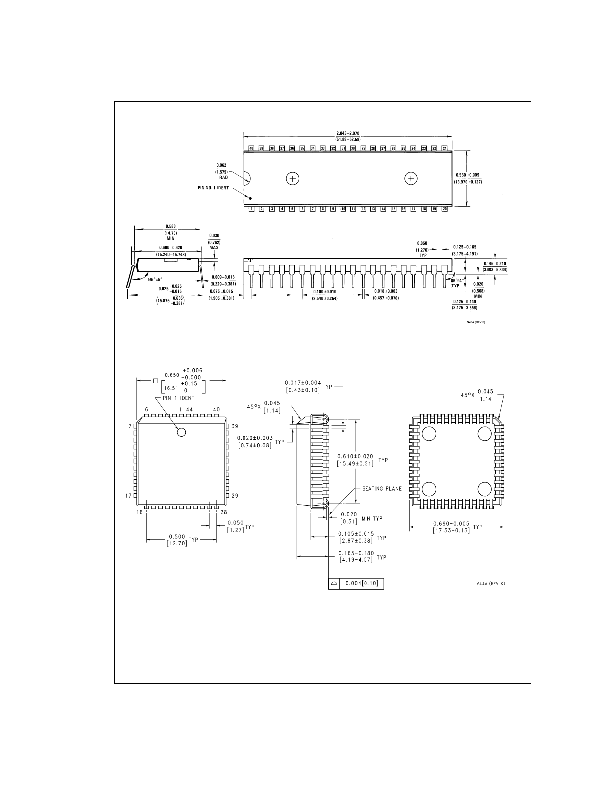
Physical Dimensions inches (millimeters) unless otherwise noted
Order Number COP688KG-XXX/N, COP888KG-XXX/N
Order Number COP688KG-XXXV, COP888KG-XXX/V
Molded Dual-In-Line Package (N)
NS Package Number N40A
Plastic Leaded Chip Carrier (V)
NS Package Number V44A
www.national.com 52
Page 53

Notes
COP888xG/CS Family, 8-Bit CMOS ROM Based Microcontrollers with 4k to 24k Memory,
Comparators and USART
LIFE SUPPORT POLICY
NATIONAL’S PRODUCTS ARE NOT AUTHORIZED FOR USE AS CRITICAL COMPONENTS IN LIFE SUPPORT
DEVICES OR SYSTEMS WITHOUT THE EXPRESS WRITTEN APPROVAL OF THE PRESIDENT AND GENERAL
COUNSEL OF NATIONAL SEMICONDUCTOR CORPORATION. As used herein:
1. Life support devices or systems are devices or
systems which, (a) are intended for surgical implant
into the body, or (b) support or sustain life, and
whose failure to perform when properly used in
accordance with instructions for use provided in the
2. A critical component is any component of a life
support device or system whose failure to perform
can be reasonably expected to cause the failure of
the life support device or system, or to affect its
safety or effectiveness.
labeling, can be reasonably expected to result in a
significant injury to the user.
National Semiconductor
Corporation
Americas
Tel: 1-800-272-9959
Fax: 1-800-737-7018
Email: [email protected]
www.national.com
National does not assume any responsibility for use of any circuitry described, no circuit patent licenses are implied and National reserves the right at any time without notice to change said circuitry and specifications.
National Semiconductor
Europe
Fax: +49 (0) 1 80-530 85 86
Email: [email protected]
Deutsch Tel: +49 (0) 1 80-530 85 85
English Tel: +49 (0) 1 80-532 78 32
Français Tel: +49 (0) 1 80-532 93 58
Italiano Tel: +49 (0) 1 80-534 16 80
National Semiconductor
Asia Pacific Customer
Response Group
Tel: 65-2544466
Fax: 65-2504466
Email: [email protected]
National Semiconductor
Japan Ltd.
Tel: 81-3-5639-7560
Fax: 81-3-5639-7507
Page 54

Copyright © Each Manufacturing Company.
All Datasheets cannot be modified without permission.
This datasheet has been download from :
www.AllDataSheet.com
100% Free DataSheet Search Site.
Free Download.
No Register.
Fast Search System.
www.AllDataSheet.com
 Loading...