

Page 1
查询COP87L20CJM-1N供应商
COP820CJ/COP822CJ/COP823CJ 8-Bit Microcontroller
with Multi-Input Wake Up and Brown Out Detector
General Description
The COP820CJ is a member of the COP8TM8-bit Microcontroller family. It is a fully static Microcontroller, fabricated
using double-metal silicon gate microCMOS technology.
This low cost Microcontroller is a complete microcomputer
containing all system timing, interrupt logic, ROM, RAM, and
I/O necessary to implement dedicated control functions in a
variety of applications. Features include an 8-bit memory
mapped architecture, MICROWIRE
timer/counter with capture register, a multi-sourced interrupt, Comparator, WATCHDOG
Brown out protection and Multi-Input Wakeup. Each I/O pin
has software selectable options to adapt the device to the
specific application. The device operates over a voltage
range of 2.5V to 6.0V. High throughput is achieved with an
efficient, regular instruction set operating at a 1 ms per instruction rate.
Key Features
Y
Multi-Input Wake Up (on the 8-bit Port L)
Y
Brown out detector
Y
Analog comparator
Y
Modulator/timer (High speed PWM for IR transmission)
Y
16-bit multi-function timer supporting
Ð PWM mode
Ð External event counter mode
Ð Input capture mode
Y
1024 bytes of ROM
Y
64 bytes of RAM
I/O Features
Y
Memory mapped I/O
TM
TM
serial I/O, a 16-bit
Timer, Modulator/Timer,
September 1996
Y
Software selectable I/O options (TRI-STATEÉoutput,
push-pull output, weak pull-up input, high impedance
input)
Y
High current outputs (8 pins)
Y
Schmitt trigger inputs on Port G
Y
MICROWIRE/PLUSTMserial I/O
Y
Packages
Ð 16 SO with 12 I/O pins
Ð 20 DIP/SO with 16 I/O pins
Ð 28 DIP/SO with 24 I/O pins
CPU/Instruction Set Feature
Y
1 ms instruction cycle time
Y
Three multi-source vectored interrupts servicing
Ð External interrupt with selectable edge
Ð Timer interrupt
Ð Software interrupt
Y
Versatile and easy to use instruction set
Y
8-bit Stack Pointer (SP)Ðstack in RAM
Y
Two 8-bit register indirect data memory pointers (B, X)
Fully Static CMOS
Y
Low current drain (typicallyk1 mA)
Y
Single supply operation: 2.5V to 6.0V
Y
Temperature range:b40§Ctoa85§C
Development Support
Y
Emulation and OTP devices
Y
Real time emulation and full program debug offered by
MetaLink Development System
COP820CJ/COP822CJ/COP823CJ 8-Bit Microcontroller
with Multi-Input Wake Up and Brown Out Detector
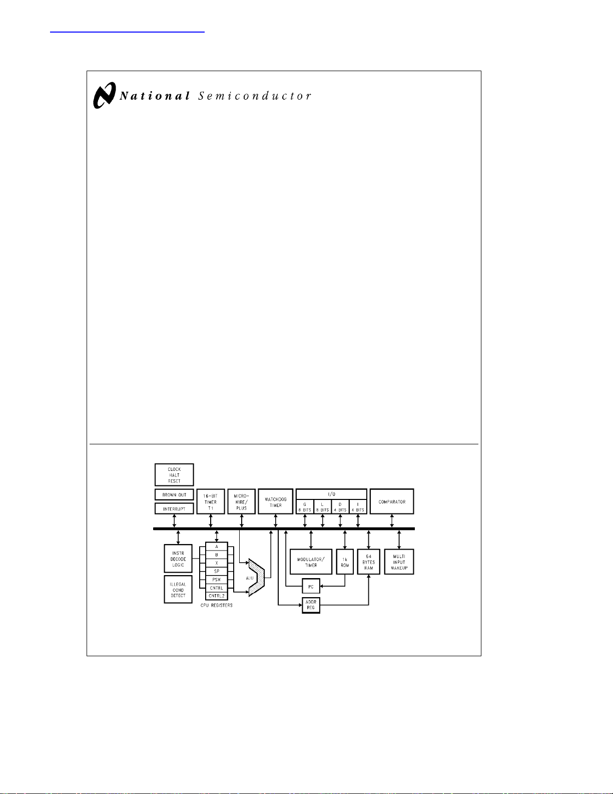
Block Diagram
FIGURE 1. Block Diagram
TRI-STATEÉis a registered trademark of National Semiconductor Corporation.
TM
COP8
Microcontrollers, MICROWIRETM, MICROWIRE/PLUSTMand WATCHDOGTMare trademarks of National Semiconductor Corporation.
TM
iceMASTER
C
1996 National Semiconductor Corporation RRD-B30M106/Printed in U. S. A.
is a trademark of MetaLink Corporation.
TL/DD11208
TL/DD/11208– 1
http://www.national.com
Page 2
COP820CJ/COP822CJ/COP823CJ
Absolute Maximum Ratings
If Military/Aerospace specified devices are required,
please contact the National Semiconductor Sales
Office/Distributors for availability and specifications.
Supply Voltage (V
Voltage at any Pin
) 7.0V
CC
b
0.3V to V
CC
a
0.3V
Total Current into VCCpin (Source) 80 mA
DC Electrical Characteristics
b
40§CsT
Parameter Conditions Min Typ Max Units
Operating Voltage Brown Out Disabled 2.5 6.0 V
Power Supply Ripple 1 (Note 1) Peak to Peak 0.1 V
Supply Current (Note 2)
e
10 MHz V
CKI
e
4 MHz V
CKI
e
4 MHz V
CKI
CKIe1 MHz V
HALT Current with Brown Out
Disbled (Note 3)
HALT Current with Brown Out V
Enabled
e
6V, tce1 ms 6.0 mA
CC
e
6V, tce2.5 ms 3.5 mA
CC
e
4.0V, tce2.5 ms 2.0 mA
CC
e
4.0V, tce10 ms 1.5 mA
CC
e
6V, CKIe0 MHz
V
CC
e
6V, CKIe0 MHz
CC
Brown Out Trip Level
(Brown Out Enabled)
INPUT LEVELS (VIH,VIL)
Reset, CKI:
Logic High 0.8 V
Logic Low 0.2 V
All Other Inputs
Logic High 0.7 V
Logic Low 0.2 V
Hi-Z Input Leakage V
Input Pullup Current V
CC
CC
e
e
6.0V
6.0V, V
IN
L- and G-Port Hysteresis (Note 5) 0.35 V
Output Current Levels
D Outputs:
e
Source V
Sink V
L4–L7 Output Sink V
All Others
Source (Weak Pull-up Mode) V
Source (Push-pull Mode) V
Sink (Push-pull Mode) V
TRI-STATE Leakage
4.5V, V
CC
e
V
CC
e
CC
e
V
CC
e
CC
e
CC
e
V
CC
e
CC
e
V
CC
e
CC
e
V
CC
2.5V, V
4.5V, V
2.5V, V
4.5V, V
4.5V, V
2.5V, V
4.5V, V
2.5V, V
4.5V, V
2.5V, V
OH
OH
OL
OH
OL
OH
OH
OH
OH
OL
OL
Allowable Sink/Source
Current Per Pin
D Outputs 15 mA
L4–L7 (Sink) 20 mA
All Others 3mA
Total Current out of GND pin (sink) 80 mA
Storage Temperature Range
Absolute maximum ratings indicate limits beyond
Note:
b
65§Ctoa150§C
which damage to the device may occur.
DC and AC electrical specifications are not ensured when
operating the device at absolute maximum ratings.
s
a
85§C unless otherwise specified
A
CC
k
110 mA
k
50 110 mA
1.8 3.1 4.2 V
CC
CC
b
2
e
0V
e
3.8V
e
1.8V
e
1.0V 10 mA
e
0.4V 2 mA
e
2.5V 15 mA
e
3.2V
e
1.8V
e
3.8V
e
1.8V
e
0.4V 1.6 mA
e
0.4V 0.7 mA
b
40
b
0.4 mA
b
0.2 mA
b
10
b
2.5
b
0.4 mA
b
0.2 mA
b
2.0
CC
CC
a
2 mA
b
250 mA
CC
b
110 mA
b
33 mA
a
2.0 mA
V
V
V
V
V
V
http://www.national.com 2
Page 3
DC Electrical Characteristics
b
40§CsT
s
a
85§C unless otherwise specified (Continued)
A
Parameter Conditions Min Typ Max Units
Maximum Input Current Room Temperature
without Latchup (Note 4)
RAM Retention Voltage, V
r
500 ns Rise and
Fall Time (Min)
2.0 V
g
100 mA
Input Capacitance 7pF
Load Capacitance on D2 1000 pF
Note 1: Rate of voltage change must be less than 10 V/mS.
Note 2: Supply current is measured after running 2000 cycles with a square wave CKI input, CKO open, inputs at rails and outputs open.
Note 3: The HALT mode will stop CKI from oscillating in the RC and crystal configurations. HALT test conditions: L, and G0..G5 ports configured as outputs and set
high. The D port set to zero. All inputs tied to V
Note 4: Pins G6 and RESET
when biased at voltages greater than VCC(the pins do not have source current when biased at a voltage below VCC). The effective resistance to VCCis 750X
V
CC
(typical). These two pins will not latch up. The voltage at the pins must be limited to less than 14V.
are designed with a high voltage input network. These pins allow input voltages greater than VCCand the pins will have sink current to
. The comparator and the Brown Out circuits are disabled.
CC
AC Electrical Characteristics
b
40§CsT
s
a
85§C unless otherwise specified
A
Parameter Conditions Min Typ Max Units
Instruction Cycle Time (tc)
s
Crystal/Resonator 4.5V
R/C Oscillator 4.5V
VCCRise Time when Using Brown Out V
Frequency at Brown Out Reset 4 MHz
s
V
6.0V 1 DC ms
CC
s
s
2.5V
V
4.5V 2.5 DC ms
CC
s
s
V
6.0V 3 DC ms
CC
s
s
2.5V
V
4.5V 7.5 DC ms
CC
e
0V to 6V 50 ms
CC
CKI Frequency For Modular Output 4 MHz
CKI Clock Duty Cycle (Note 5) freMax 40 60 %
Rise Time (Note 5) fr
Fall Time (Note 5) fr
e
10 MHz ext. Clock 12 ns
e
10 MHz ext. Clock 8 ns
Inputs
t
Setup
t
Hold
Output Propagation Delay R
t
PD1,tPD0
SO, SK 4.5VsV
4.5VsV
2.5V
4.5VsV
2.5V
L
2.5VsV
All Others 4.5V
2.5V
s
6.0V 200 ns
CC
s
s
V
4.5V 500 ns
CC
s
6.0V 60 ns
CC
s
s
V
4.5V 150 ns
CC
e
2.2k, CLe100 pF
s
6.0V 0.7 ms
CC
s
4.5V 1.75 ms
CC
s
s
V
6.0V 1 ms
CC
s
s
V
4.5V 5 ms
CC
Input Pulse Width
Interrupt Input High Time 1 tc
Interrupt Input Low Time 1 tc
Timer Input High Time 1 tc
Timer Input Low Time 1 tc
MICROWIRE Setup Time (t
MICROWIRE Hold Time (t
MICROWIRE Output
Propagation Delay (t
mPD
)20ns
mWS
)56ns
mWH
)
220 ns
Reset Pulse Width 1.0 ms
Note 5: Parameter characterized but not production tested.
http://www.national.com3
Page 4
AC Electrical Characteristics (Continued)
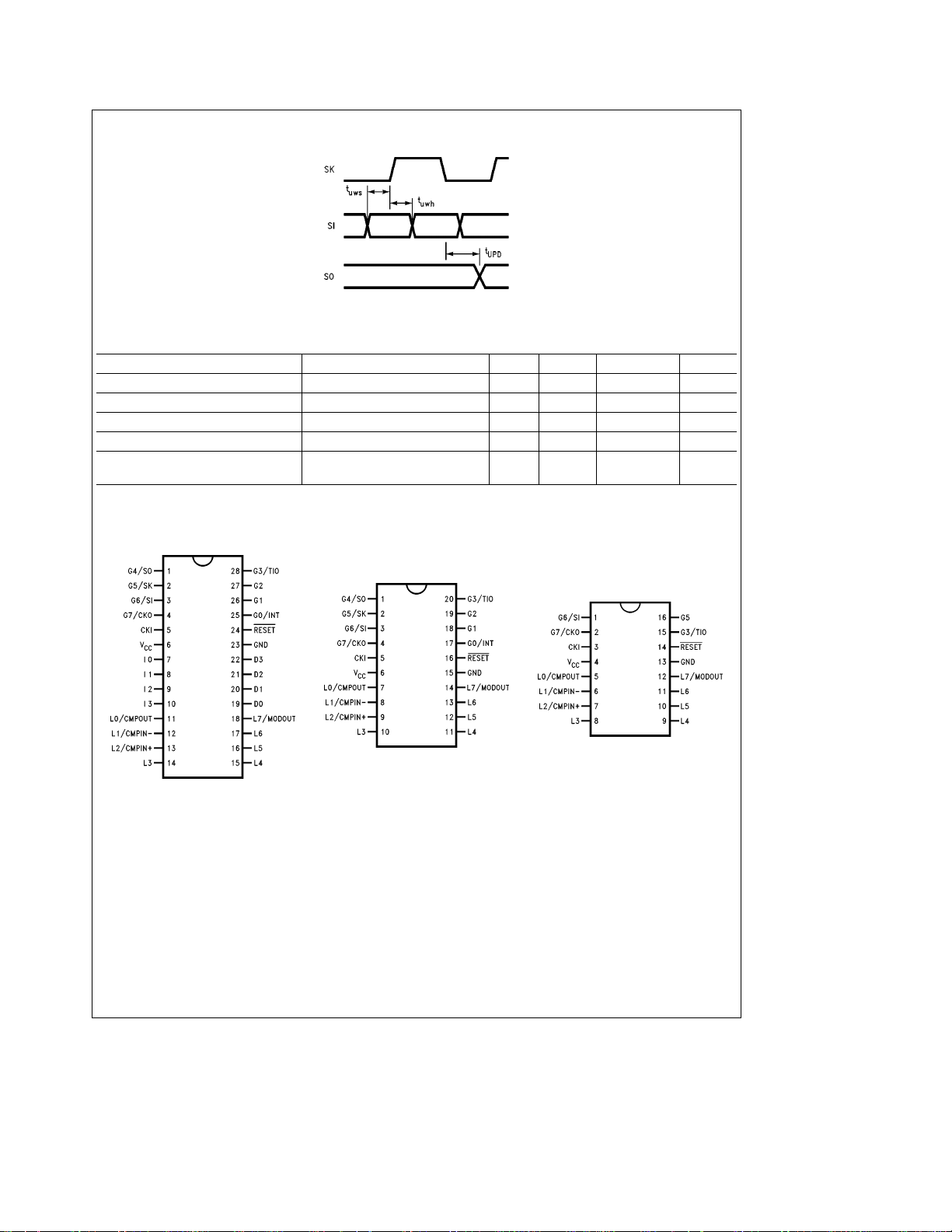
FIGURE 2. MICROWIRE/PLUS Timing
TL/DD/11208– 2
Comparator DC and AC Characteristics 4V
s
s
V
6V,b40§CsT
CC
s
A
a
85§C (Note 1)
Parameters Conditions Min Type Max Units
k
Input Offset Voltage 0.4VkV
IN
b
V
1.5V
CC
Input Common Mode Voltage Range 0.4 V
g
10
g
25 mV
b
1.5 V
CC
Voltage Gain 300k V/V
DC Supply Current (when enabled) V
Response Time TBD mV Step,
Note 1: For comparator output current characteristics see L-Port specs.
e
6.0V 250 mA
CC
TBD mV Overdrive, 100 pF Load
1 ms
Connection Diagrams
Top View
Top View
TL/DD/11208– 3
Order Number COPCJ822-XXX/N or
COPCJ822-XXX/WM
Order Number COPCJ820-XXX/N or
COPCJ820-XXX/WM
FIGURE 3. Connection Diagrams
http://www.national.com 4
TL/DD/11208– 4
Top View
TL/DD/11208– 5
Order Number COPCJ823-XXX/WM
Page 5
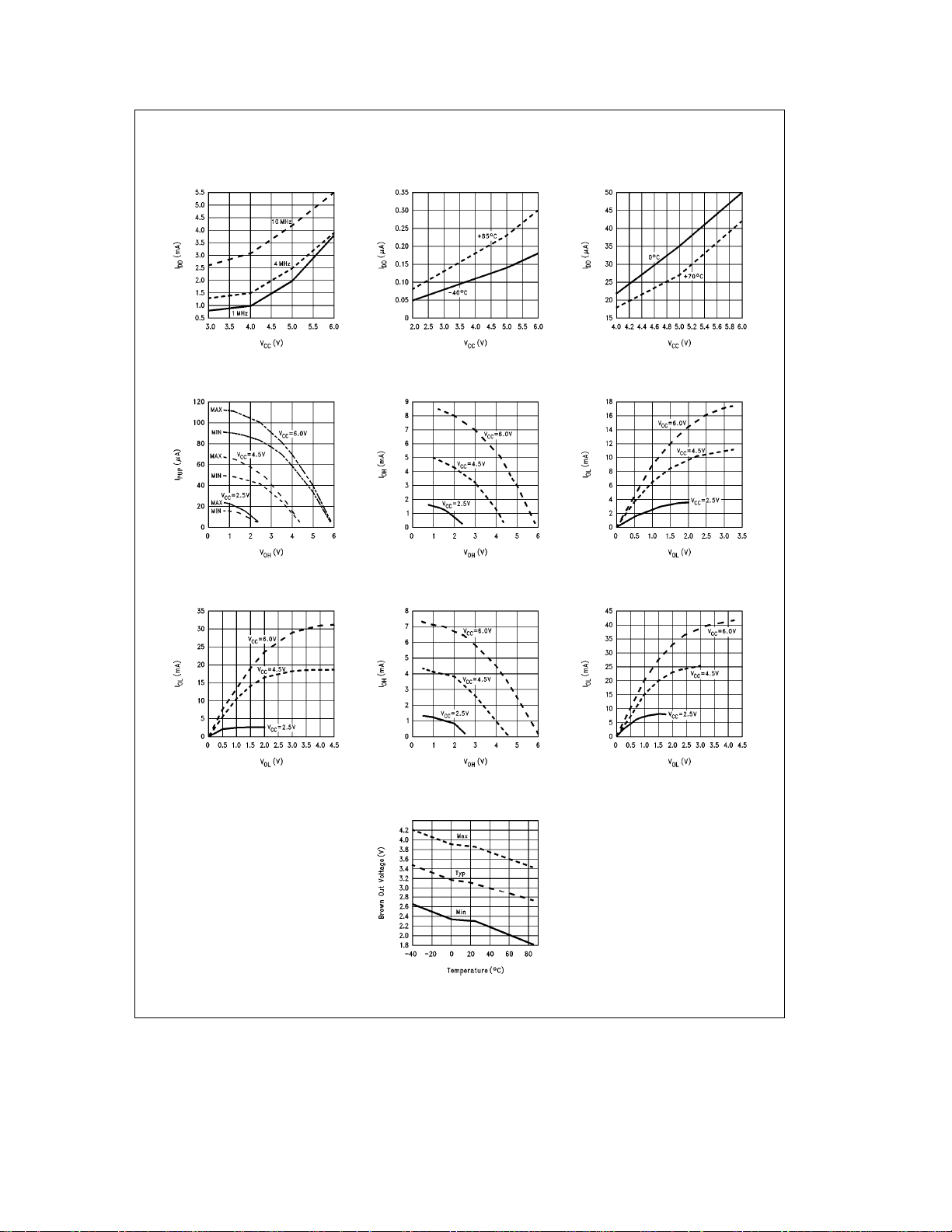
Typical Performance Characteristics
DynamicÐI
(Crystal Clock Option)
DD
vs V
CC
Ports L/G Weak
Pull-Up Source Current
Ports L4–L7
Sink Current
DD
vs V
CC
HaltÐI
(Brown Out Disabled)
Ports L/G Push-Pull
Source Current
HaltÐI
(Brown Out Enabled)
Ports L/G Push-Pull
Sink Current
DD
vs V
CC
Port D Source Current Port D Sink Current
Brown Out Voltage
vs Temperature
TL/DD/11208– 28
http://www.national.com5
Page 6
COP820CJ Pin Assignment
Port
Typ
Pin Funct. Pin Pin Pin
L0 I/O MIWU/CMPOUT 5 7 11
L1 I/O MIWU/CMPIN
L2 I/O MIWU/CMPIN
L3 I/O MIWU 8 10 14
L4 I/O MIWU 9 11 15
L5 I/O MIWU 10 12 16
L6 I/O MIWU 11 13 17
L7 I/O MIWU/MODOUT 12 14 18
G0 I/O INTR 17 25
G1 I/O 18 26
G2 I/O 19 27
G3 I/O TIO 15 20 28
G4 I/O SO 1 1
G5 I/O SK 16 2 2
G6 ISI 133
G7 I CKO 2 4 4
I0 I 7
I1 I 8
I2 I 9
I3 I 10
D0 O 19
D1 O 20
D2 O 21
D3 O 22
V
CC
GND 13 15 23
CKI 3 5 5
RESET 14 16 24
ALT 16 20 28
b
6812
a
7913
466
Pin Description
VCCand GND are the power supply pins.
CKI is the clock input. This can come from an external
source, a R/C generated oscillator or a crystal (in conjunction with CKO). See Oscillator description.
RESET
is the master reset input. See Reset description.
PORT I is a 4-bit Hi-Z input port.
PORT L is an 8-bit I/O port.
There are two registers associated with the L port: a data
register and a configuration register. Therefore, each L
I/O bit can be individually configured under software control
as shown below:
Port L Port L Port L
Config. Data Setup
0 0 Hi-Z Input (TRI-STATE)
0 1 Input with Weak Pull-up
1 0 Push-pull Zero Output
1 1 Push-pull One Output
Three data memory address locations are allocated for this
port, one each for data register[00D0], configuration register[00D1]and the input pins[00D2].
Port L has the following alternate features:
L0 MIWU or CMPOUT
L1 MIWU or CMPIN
L2 MIWU or CMPIN
L3 MIWU
L4 MIWU (high sink current capability)
L5 MIWU (high sink current capability)
L6 MIWU (high sink current capability)
L7 MIWU or MODOUT (high sink current capability)
The selection of alternate Port L functions is done through
registers WKEN[00C9]to enable MIWU and CNTRL2
[
00CC]to enable comparator and modulator.
All eight L-pins have Schmitt Triggers on their inputs.
PORT G is an 8-bit port with 6 I/O pins (G0–G5) and 2 input
pins (G6, G7).
All eight G-pins have Schmitt Triggers on the inputs.
There are two registers associated with the G port: a data
register and a configuration register. Therefore each G port
bit can be individually configured under software control as
shown below:
Port G Port G Port G
Config. Data Setup
0 0 Hi-Z Input (TRI-STATE)
0 1 Input with Weak Pull-up
1 0 Push-pull Zero Output
1 1 Push-pull One Output
Three data memory address locations are allocated for this
port, one for data register[00D3], one for configuration register[00D5]and one for the input pins[00D6]. Since G6
and G7 are Hi-Z input only pins, any attempt by the user to
configure them as outputs by writing a one to the configuration register will be disregarded. Reading the G6 and G7
configuration bits will return zeros. Note that the device will
be placed in the Halt mode by writing a ‘‘1’’ to the G7 data
bit.
Six pins of Port G have alternate features:
G0 INTR (an external interrupt)
G3 TIO (timer/counter input/output)
G4 SO (MICROWIRE serial data output)
G5 SK (MICROWIRE clock I/O)
G6 SI (MICROWIRE serial data input)
G7 CKO crystal oscillator output (selected by mask option)
or HALT restart input/general purpose input (if clock
option is R/C or external clock)
b
a
http://www.national.com 6
Page 7
Pin Description (Continued)
Pins G1 and G2 currently do not have any alternate functions.
The selection of alternate Port G functions are done through
registers PSW[00EF]to enable external interrupt and
CNTRL1[00EE]to select TIO and MICROWIRE operations.
PORT D is a four bit output port that is preset when RESET
goes low. One data memory address location is allocated
for the data register[00DC].
Note: Care must be exercised with the D2 pin operation. At RESET, the
external loads on this pin must ensure that the output voltages stay above
to prevent the chip from entering special modes. Also keep the
0.8 V
CC
external loading on D2 to less than 1000 pF.
Functional Description
The internal architecture is shown in the block diagram.
Data paths are illustrated in simplified form to depict how
the various logic elements communicate with each other in
implementing the instruction set of the device.
ALU and CPU Registers
The ALU can do an 8-bit addition, subtraction, logical or
shift operations in one cycle time. There are five CPU registers:
A is the 8-bit Accumulator register
PC is the 15-bit Program Counter register
PU is the upper 7 bits of the program counter (PC)
PL is the lower 8 bits of the program counter (PC)
B is the 8-bit address register and can be auto incre-
mented or decremented.
X is the 8-bit alternate address register and can be auto
incremented or decremented.
SP is the 8-bit stack pointer which points to the subrou-
tine stack (in RAM).
B, X and SP registers are mapped into the on chip RAM.
The B and X registers are used to address the on chip RAM.
The SP register is used to address the stack in RAM during
subroutine calls and returns. The SP must be preset by software upon initialization.
Memory
The memory is separated into two memory spaces: program
and data.
PROGRAM MEMORY
Program memory consists of 1024 x 8 ROM. These bytes of
ROM may be instructions or constant data. The memory is
addressed by the 15-bit program counter (PC). ROM can be
indirectly read by the LAID instruction for table lookup.
DATA MEMORY
The data memory address space includes on chip RAM, I/O
and registers. Data memory is addressed directly by the instruction or indirectly through B, X and SP registers. The
device has 64 bytes of RAM. Sixteen bytes of RAM are
mapped as ‘‘registers’’, these can be loaded immediately,
decremented and tested. Three specific registers: X, B, and
SP are mapped into this space, the other registers are available for general usage.
Any bit of data memory can be directly set, reset or tested.
All I/O and registers (except A and PC) are memory
mapped; therefore, I/O bits and register bits can be directly
and individually set, reset and tested, except the write once
only bit (WDREN, WATCHDOG Reset Enable), and the unused and read only bits in CNTRL2 and WDREG registers.
Note: RAM contents are undefined upon power-up.
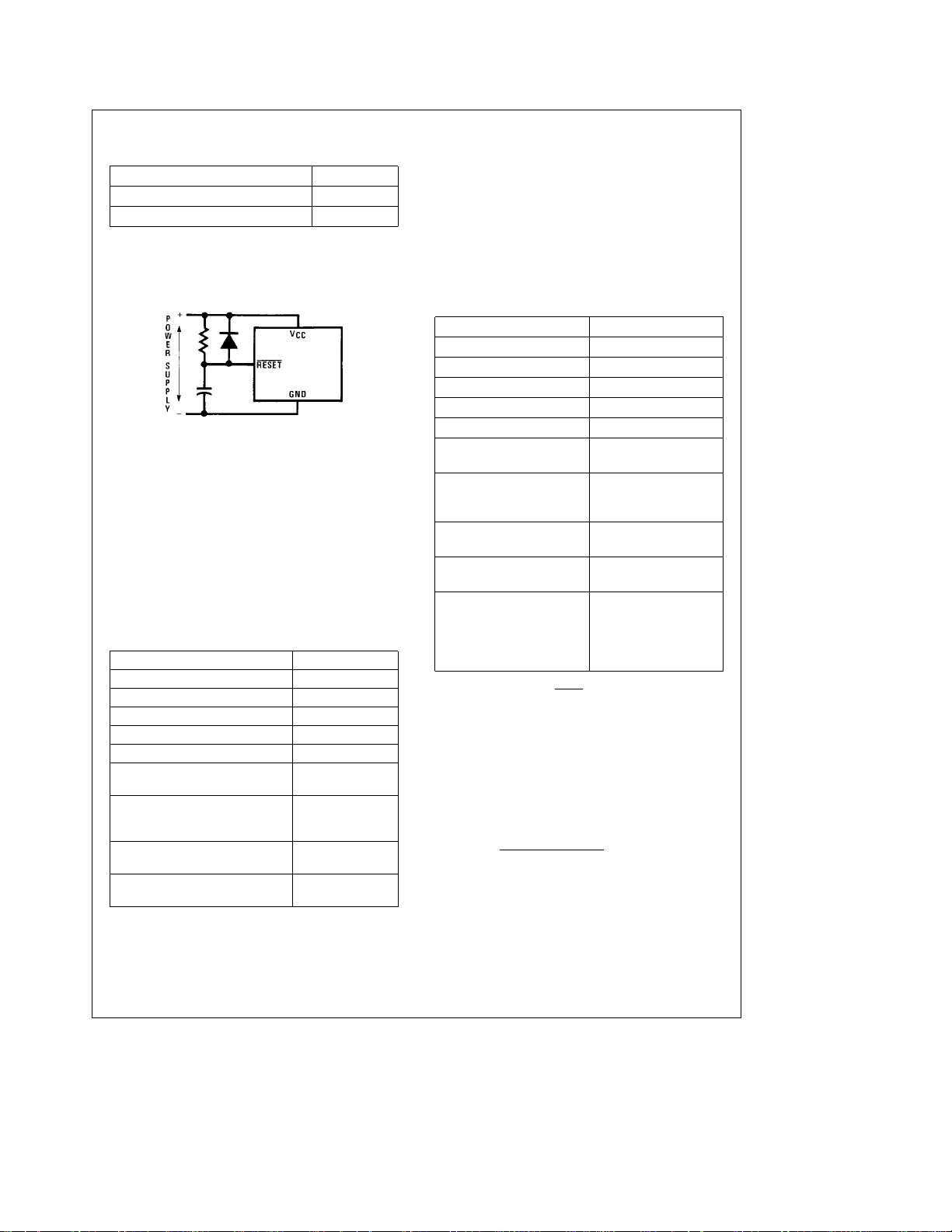
Reset
EXTERNAL RESET
The RESET input pin when pulled low initializes the microcontroller. The user must insure that the RESET pin is held
low until V
clock is stabilized. An R/C circuit with a delay 5x greater
than the power supply rise time is recommended
The device immediately goes into reset state when the
RESET input goes low. When the RESET pin goes high the
device comes out of reset state synchronously. The device
will be running within two instruction cycles of the RESET
pin going high. The following actions occur upon reset:
Port L TRI-STATE
Port G TRI-STATE
Port D HIGH
PC CLEARED
RAM Contents RANDOM with Power-On-
B, X, SP Same as RAM
PSW, CNTRL1, CNTRL2
and WDREG Reg. CLEARED
Multi-Input Wakeup Reg.
WKEDG, WKEN CLEARED
WKPND UNKNOWN
Data and Configuration
Registers forL&G CLEARED
WATCHDOG Timer Prescaler/Counter each
The device comes out of the HALT mode when the RESET
pin is pulled low. In this case, the user has to ensure that the
RESET signal is low long enough to allow the oscillator to
restart. An internal 256 t
tion with the two pin crystal oscillator. When the device
comes out of the HALT mode through Multi-Input Wakeup,
this delay allows the oscillator to stabilize.
The following additional actions occur after the device
comes out of the HALT mode through the RESET pin.
If a two pin crystal/resonator oscillator is being used:
RAM Contents UNCHANGED
Timer T1 and A Contents UNKNOWN
WATCHDOG Timer Prescaler/Counter ALTERED
is within the specified voltage range and the
CC
(Figure 4)
Reset
UNAFFECTED with external
Reset (power already applied)
loaded with FF
delay is normally used in conjunc-
c
.
http://www.national.com7
Page 8
Functional Description (Continued)
If the external or RC Clock option is being used:
RAM Contents UNCHANGED
Timer T1 and A Contents UNCHANGED
WATCHDOG Timer Prescaler/Counter ALTERED
The external RESET takes priority over the Brown Out Reset.
Note: If the RESET pin is pulled low while Brown Out occurs (Brown Out
circuit has detected Brown Out condition), the external reset will not
occur until the Brown Out condition is removed. External reset has
priority only if V
RCl5cPower Supply Rise Time TL/DD/11208– 6
FIGURE 4. Recommended Reset Circuit
WATCHDOG RESET
With WATCHDOG enabled, the WATCHDOG logic resets
the device if the user program does not service the WATCHDOG timer within the selected service window. The
WATCHDOG reset does not disable the WATCHDOG.
Upon WATCHDOG reset, the WATCHDOG Prescaler/
Counter are each initialized with FF Hex.
The following actions occur upon WATCHDOG reset that
are different from external reset.
WDREN WATCHDOG Reset Enable bit UNCHANGED
WDUDF WATCHDOG Underflow bit UNCHANGED
Additional initialization actions that occur as a result of
WATCHDOG reset are as follows:
Port L TRI-STATE
Port G TRI-STATE
Port D HIGH
PC CLEARED
Ram Contents UNCHANGED
B, X, SP UNCHANGED
PSW, CNTRL1 and CNTRL2 (except
WDUDF Bit) Registers CLEARED
Multi-Input Wakeup Registers
WKEDG, WKEN CLEARED
WKPND UNKNOWN
Data and Configuration
Registers forL&G CLEARED
WATCHDOG Timer Prescalar/Counter
BROWN OUT RESET
The on-board Brown Out protection circuit resets the device
when the operating voltage (V
Out voltage. The device is held in reset when V
below the Brown Out Voltage. The device will remain in
is greater than the Brown Out voltage.
CC
each loaded with FF
) is lower than the Brown
CC
CC
stays
RESET as long as V
Device will resume execution if V
Out Voltage. If a two pin crystal/resonator clock option is
is below the Brown Out Voltage. The
CC
rises above the Brown
CC
selected, the Brown Out reset will trigger a 256tc delay. This
delay allows the oscillator to stabilize before the device exits the reset state. The delay is not used if the clock option is
either R/C or external clock. The contents of data registers
and RAM are unknown following a Brown Out reset. The
external reset takes priority over Brown Out Reset and will
deactivate the 256 tc cycles delay if in progress. The Brown
Out reset takes priority over the WATCHDOG reset.
The following actions occur as a result of Brown Out reset:
Port L TRI-STATE
Port G TRI-STATE
Port D HIGH
PC CLEARED
RAM Contents RANDOM
B, X, SP UNKNOWN
PSW, CNTRL1, CNTRL2
and WDREG Registers CLEARED
Multi-Input Wakeup Registers
WKEDG, WKEN CLEARED
WKPND UNKNOWN
Data and Configuration
Registers forL&G CLEARED
WATCHDOG Timer Prescalar/Counter each
loaded with FF
Timer T1 and Accumulator Unknown data after
coming out of the HALT
(through Brown Out
Reset) with any Clock
option
Note: The development system will detect the BROWN OUT RESET exter-
nally and will force the RESET
does not emulate the 256tc delay.
pin low. The Development System
Brown Out Detection
An on-board detection circuit monitors the operating voltage
(V
) and compares it with the minimum operating voltage
CC
specified. The Brown Out circuit is designed to reset the
device if the operating voltage is below the Brown Out voltage (between 1.8V to 4.2V at
b
40§Ctoa85§C). The Minimum operating voltage for the device is 2.5V with Brown
Out disabled, but with BROWN OUT enabled the device is
guaranteed to operate properly down to minimum Brown
Out voltage (Max frequency 4 MHz
of 0
Cto70§C the Brown Out voltage is expected to be
§
between 1.9V to 3.9V. The circuit can be enabled or dis-
), For temperature range
abled by Brown Out mask option. If the device is intended to
operate at lower V
max), the Brown Out circuit should be disabled by the mask
(lower than Brown Out voltage VBO
CC
option.
The Brown Out circuit may be used as a power-up reset
provided the power supply rise time is slower than 50 ms (0V
to 6.0V).
Note: Brown Out Circuit is active in HALT mode (with the Brown Out mask
option selected).
http://www.national.com 8
Page 9
Functional Description (Continued)
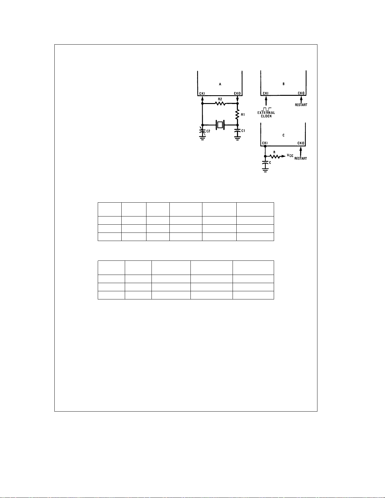
Oscillator Circuits
EXTERNAL OSCILLATOR
CKI can be driven by an external clock signal provided it
meets the specified duty cycle, rise and fall times, and input
levels. CKO is available as a general purpose input G7
and/or Halt control.
CRYSTAL OSCILLATOR
By selecting CKO as a clock output, CKI and CKO can be
connected to create a crystal controlled oscillator. Table I
shows the component values required for various standard
crystal values.
R/C OSCILLATOR
By selecting CKI as a single pin oscillator, CKI can make a
R/C oscillator. CKO is available as a general purpose input
and/or HALT control. Table II shows variation in the oscillator frequencies as functions of the component (R and C)
values.
FIGURE 5. Clock Oscillator Configurations
TABLE I. Crystal Oscillator Configuration
R1 R2 C1 C2 CKI Freq.
(kX)(MX) (pF) (pF) (MHz)
0 1 30 30– 36 10 V
0 1 30 30– 36 4 V
5.6 1 100 100 –156 0.455 V
TABLE II. RC Oscillator Configuration (Part-To-Part Variation)
R C CK1 Freq. Instr. Cycle
(kX) (pF) (MHz) (ms)
3.3 82 2.2 to 2.7 3.7 to 4.6 V
5.6 100 1.1 to 1.3 7.4 to 9.0 V
6.8 100 0.9 to 1.1 8.8 to 10.8 V
Conditions
e
CC
e
CC
e
CC
Conditions
e
5V
CC
e
5V
CC
e
5V
CC
TL/DD/11208– 7
5V
5V
5V
http://www.national.com9
Page 10

Functional Description (Continued)
Halt Mode
The device is a fully static device. The device enters the
HALT mode by writing a one to the G7 bit of the G data
register. Once in the HALT mode, the internal circuitry does
not receive any clock signal and is therefore frozen in the
exact state it was in when halted. In this mode the chip will
only draw leakage current (output current and DC current
due to the Brown Out circuit if Brown Out is enabled).
The device supports four different methods of exiting the
HALT mode. The first method is with a low to high transition
on the CKO (G7) pin. This method precludes the use of the
crystal clock configuration (since CKO is a dedicated output). It may be used either with an RC clock configuration or
an external clock configuration. The second method of exiting the HALT mode is with the multi-Input Wakeup feature
on the L port. The third method of exiting the HALT mode is
by pulling the RESET input low. The fourth method is with
the operating voltage going below Brown Out voltage (if
Brown Out is enabled by mask option).
If the two pin crystal/resonator oscillator is being used and
Multi-Input Wakeup or Brown Out causes the device to exit
the HALT mode, the WAKEUP signal does not allow the
chip to start running immediately since crystal oscillators
have a delayed start up time to reach full amplitude and
freuqency stability. The WATCHDOG timer (consisting of an
8-bit prescaler followed by an 8-bit counter) is used to generate a fixed delay of 256tc to ensure that the oscillator has
indeed stabilized before allowing instruction execution. In
this case, upon detecting a valid WAKEUP signal only the
oscillator circuitry is enabled. The WATCHDOG Counter and
Prescaler are each loaded with a value of FF Hex. The
WATCHDOG prescaler is clocked with the tc instruction cycle. (The tc clock is derived by dividing the oscillator clock
down by a factor of 10). The Schmitt trigger following the
CKI inverter on the chip ensures that the WATCHDOG timer
is clocked only when the oscillator has a sufficiently large
amplitude to meet the Schmitt trigger specs. This Schmitt
trigger is not part of the oscillator closed loop. The start-up
timeout from the WATCHDOG timer enables the clock signals to be routed to the rest of the chip. The delay is not
activated when the device comes out of HALT mode
through RESET pin. Also, if the clock option is either RC or
External clock, the delay is not used, but the WATCHDOG
Prescaler/-Counter contents are changed. The Development System will not emulate the 256tc delay.
The RESET
pin or Brown Out will cause the device to reset
and start executing from address X’0000. A low to high transition on the G7 pin (if single pin oscillator is used) or MultiInput Wakeup will cause the device to start executing from
the address following the HALT instruction.
When RESET
pin is used to exit the device from the HALT
mode and the two pin crystal/resonator (CKI/CKO) clock
option is selected, the contents of the Accumulator and the
Timer T1 are undetermined following the reset. All other
information except the WATCHDOG Prescaler/Counter
contents is retained until continuing. If the device comes out
of the HALT mode through Brown Out reset, the contents of
data registers and RAM are unknown following the reset. All
information except the WATCHDOG Prescaler/Counter
contents is retained if the device exits the HALT mode
through G7 pin or Multi-Input Wakeup.
G7 is the HALT-restart pin, but it can still be used as an
input. If the device is not halted, G7 can be used as a general purpose input.
If the Brown Out Enable mask option is selected, the Brown
Out circuit remains active during the HALT mode causing
additional current to be drawn.
Note: To allow clock resynchronization, it is necessary to program two
NOP’s immediately after the device comes out of the HALT mode.
The user must program two NOP’s following the ‘‘enter HALT mode’’
(set G7 data bit) instruction.
http://www.national.com 10
Page 11

Functional Description (Continued)
MICROWIRE/PLUS
MICROWIRE/PLUS is a serial synchronous bidirectional
communications interface. The MICROWIRE/PLUS capability enables the device to interface with any of National
Semiconductor’s MICROWIRE peripherals (i.e. A/D converters, display drivers, EEPROMS, etc.) and with other microcontrollers which support the MICROWIRE/PLUS interface. It consists of an 8-bit serial shift register (SIO) with
serial data input (SI), serial data output (SO) and serial shift
clock (SK).
WIRE/PLUS interface.
The shift clock can be selected from either an internal
source or an external source. Operating the MICROWIRE/
PLUS interface with the internal clock source is called the
Master mode of operation. Operating the MICROWIRE/
PLUS interface with an external shift clock is called the
Slave mode of operation.
The CNTRL register is used to configure and control the
MICROWIRE/PLUS mode. To use the MICROWIRE/PLUS ,
the MSEL bit in the CNTRL register is set to one. The SK
clock rate is selected by the two bits, SL0 and SL1, in the
CNTRL register. Table III details the different clock rates
that may be selected.
Figure 6
shows the block diagram of the MICRO-
TL/DD/11208– 8
FIGURE 6. MICROWIRE/PLUS Block Diagram
TABLE III
SL1 SL0 SK Cycle Time
00 2t
01 4t
1x 8t
c
c
c
where,
tcis the instruction cycle time.
MICROWIRE/PLUS OPERATION
Setting the BUSY bit in the PSW register causes the MICROWIRE/PLUS arrangement to start shifting the data. It
gets reset when eight data bits have been shifted. The user
may reset the BUSY bit by software to allow less than 8 bits
to shift. The device may enter the MICROWIRE/PLUS
mode either as a Master or as a Slave.
Figure 7
shows how
two device microcontrollers and several peripherals may be
interconnected using the MICROWIRE/PLUS arrangement.
Master MICROWIRE/PLUS Operation
In the MICROWIRE/PLUS Master mode of operation the
shift clock (SK) is generated internally by the device. The
MICROWIRE/PLUS Master always initiates all data exchanges
(Figure 7).
The MSEL bit in the CNTRL register
must be set to enable the SO and SK functions on the G
Port. The SO and SK pins must also be selected as outputs
by setting appropriate bits in the Port G configuration register. Table IV summarizes the bit settings required for Master
mode of operation.
SLAVE MICROWIRE/PLUS OPERATION
In the MICROWIRE/PLUS Slave mode of operation the SK
clock is generated by an external source. Setting the MSEL
bit in the CNTRL register enables the SO and SK functions
on the G Port. The SK pin must be selected as an input and
the SO pin selected as an output pin by appropriately setting
up the Port G configuration register. Table IV summarizes
the settings required to enter the Slave mode of operation.
FIGURE 7. MICROWIRE/PLUS Application
TL/DD/11208– 23
http://www.national.com11
Page 12

Functional Description (Continued)
The user must set the BUSY flag immediately upon entering
the Slave mode. This will ensure that all data bits sent by
the Master will be shifted properly. After eight clock pulses
the BUSY flag will be cleared and the sequence may be
repeated.
TABLE IV
G4 G5
Config. Config.
Bit Bit
1 1 SO Int. SK SI MICROWIRE Master
0 1 TRI-STATE Int. SK SI MICROWIRE Master
1 0 SO Ext. SK SI MICROWIRE Slave
0 0 TRI-STATE Ext. SK SI MICROWIRE Slave
G4 G5 G6
Fun. Fun. Fun.
Operation
Timer/Counter
The device has a powerful 16-bit timer with an associated
16-bit register enabling it to perform extensive timer functions. The timer T1 and its register R1 are each organized
as two 8-bit read/write registers. Control bits in the register
CNTRL allow the timer to be started and stopped under
software control. The timer-register pair can be operated in
one of three possible modes. Table V details various timer
operating modes and their requisite control settings.
MODE 1. TIMER WITH AUTO-LOAD REGISTER
In this mode of operation, the timer T1 counts down at the
instruction cycle rate. Upon underflow the value in the register R1 gets automatically reloaded into the timer which continues to count down. The timer underflow can be programmed to interrupt the microcontroller. A bit in the control
register CNTRL enables the TIO (G3) pin to toggle upon
timer underflows. This allows the generation of square-wave
outputs or pulse width modulated outputs under software
control
(Figure 8)
.
MODE 2. EXTERNAL COUNTER
In this mode, the timer T1 becomes a 16-bit external event
counter. The counter counts down upon an edge on the TIO
pin. Control bits in the register CNTRL program the counter
to decrement either on a positive edge or on a negative
edge. Upon underflow the contents of the register R1 are
automatically copied into the counter. The underflow can
also be programmed to generate an interrupt
(Figure 9)
.
FIGURE 8. Timer/Counter Auto
TL/DD/11208– 24
Reload Mode Block Diagram
TABLE V. Timer Operating Modes
CNTRL Timer
Bits Operation Mode T Interrupt Counts
765 On
0 0 0 External Counter w/Auto-Load Reg. Timer Underflow TIO Pos. Edge
0 0 1 External Counter w/Auto-Load Reg. Timer Underflow TIO Neg. Edge
0 1 0 Not Allowed Not Allowed Not Allowed
0 1 1 Not Allowed Not Allowed Not Allowed
1 0 0 Timer w/Auto-Load Reg. Timer Underflow t
1 0 1 Timer w/Auto-Load Reg./Toggle TIO Out Timer Underflow t
1 1 0 Timer w/Capture Register TIO Pos. Edge t
1 1 1 Timer w/Capture Register TIO Neg. Edge t
c
c
c
c
FIGURE 9. Timer in External Event Counter Mode
http://www.national.com 12
TL/DD/11208– 29
Page 13

Timer/Counter (Continued)
MODE 3. TIMER WITH CAPTURE REGISTER
Timer T1 can be used to precisely measure external frequencies or events in this mode of operation. The timer T1
counts down at the instruction cycle rate. Upon the occurrence of a specified edge on the TIO pin the contents of the
timer T1 are copied into the register R1. Bits in the control
register CNTRL allow the trigger edge to be specified either
as a positive edge or as a negative edge. In this mode the
user can elect to be interrupted on the specified trigger
edge
(Figure 10)
FIGURE 10. Timer Capture Mode Block Diagram
TIMER PWM APPLICATION
Figure 11
can be built out of the Timer-Register pair in the Auto-Reload mode. The timer is placed in the ‘‘Timer with auto reload’’ mode and the TIO pin is selected as the timer output.
At the outset the TIO pin is set high, the timer T1 holds the
on time and the register R1 holds the signal off time. Setting
TRUN bit starts the timer which counts down at the instruction cycle rate. The underflow toggles the TIO output and
copies the off time into the timer, which continues to run. By
alternately loading in the on time and the off time at each
successive interrupt a PWM frequency can be easily generated.
.
TL/DD/11208– 25
shows how a minimal component D/A converter
Watchdog
The device has an on-board 8-bit WATCHDOG timer. The
timer contains an 8-bit READ/WRITE down counter clocked
by an 8-bit prescaler. Under software control the timer can
be dedicated for the WATCHDOG or used as a general purpose counter.
diagram.
MODE 1: WATCHDOG TIMER
The WATCHDOG is designed to detect user programs getting stuck in infinite loops resulting in loss of program control or ‘‘runaway’’ programs. The WATCHDOG can be enabled or disabled (only once) after the device is reset as a
result of brown out reset or external reset. On power-up the
WATCHDOG is disabled. The WATCHDOG is enabled by
writing a ‘‘1’’ to WDREN bit (resides in WDREG register).
Once enabled, the user program should write periodically
into the 8-bit counter before the counter underflows. The
8-bit counter (WDCNT) is memory mapped at address 0CE
Hex. The counter is loaded with n-1 to get n counts. The
counter underflow resets the device, but does not disable
the WATCHDOG. Loading the 8-bit counter initializes the
prescaler with FF Hex and starts the prescaler/counter.
Prescaler and counter are stopped upon counter underflow.
Prescaler and counter are each loaded with FF Hex when
the device goes into the HALT mode. The prescaler is used
for crystal/resonator start-up when the device exits the
HALT mode through Multi-Input Wakeup. In this case, the
prescaler/counter contents are changed.
MODE 2: TIMER
In this mode, the prescaler/counter is used as a timer by
keeping the WDREN (WATCHDOG reset enable) bit at 0.
The counter underflow sets the WDUDF (underflow) bit and
the underflow does not reset the device. Loading the 8-bit
counter (load n-1 for n counts) sets the WDTEN bit
(WATCHDOG Timer Enable) to ‘‘1’’, loads the prescaler
with FF, and starts the timer. The counter underflow stops
the timer. The WDTEN bit serves as a start bit for the
WATCHDOG timer. This bit is set when the 8-bit counter is
loaded by the user program. The load could be as a result of
WATCHDOG service (WATCHDOG timer dedicated for
WATCHDOG function) or write to the counter (WATCHDOG
timer used as a general purpose counter). The bit is cleared
upon Brown Out reset, WATCHDOG reset or external reset.
The bit is not memory mapped and is transparent to the
user program.
Figure 12
shows the WATCHDOG timer block
FIGURE 11. Timer Application
Parameter
8-Bit Prescaler FF FF FF FF
8-Bit WD Counter FF FF FF User Value
WDREN Bit Unchanged Unchanged 0 No Effect
WDUDF Bit 0 Unchanged 0 0
WDTEN Signal Unchanged 0 0 1
Note 1: BOR is Brown Out Reset.
TL/DD/11208– 26
TABLE VI. WATCHDOG Control/Status
HALT WD
Mode Reset
EXT/BOR
Reset
(Note 1)
http://www.national.com13
Counter
Load
Page 14

Functional Description (Continued)
CONTROL/STATUS BITS
WDUDF: WATCHDOG Timer Underflow Bit
This bit resides in the CNTRL2 Register. The bit is set when
the WATCHDOG timer underflows. The underflow resets
the device if the WATCHDOG reset enable bit is set
(WDREN
er underflow flag. The bit is cleared upon Brown-Out reset,
external reset, load to the 8-bit counter, or going into the
HALT mode. It is a read only bit.
e
1). Otherwise, WDUDF can be used as the tim-
WDREN: WD Reset Enable
WDREN bit resides in a separate register (bit 0 of WDREG).
This bit enables the WATCHDOG timer to generate a reset.
The bit is cleared upon Brown Out reset, or external reset.
The bit under software control can be written to only once
(once written to, the hardware does not allow the bit to be
changed during program execution).
e
WDREN
WDREN
1 WATCHDOG reset is enabled.
e
0 WATCHDOG reset is disabled.
Table VI shows the impact of Brown Out Reset, WATCHDOG Reset, and External Reset on the Control/Status bits.
FIGURE 12. WATCHDOG Timer Block Diagram
http://www.national.com 14
TL/DD/11208– 15
Page 15

Modulator/Timer
The Modulator/Timer contains an 8-bit counter and an 8-bit
autoreload register (MODRL address 0CF Hex). The Modulator/Timer has two modes of operation, selected by the
control bit MC3. The Modulator/Timer Control bits MC1,
MC2 and MC3 reside in CNTRL2 Register.
MODE 1: MODULATOR
The Modulator is used to generate high frequency pulses on
the modulator output pin (L7). The L7 pin should be configured as an output. The number of pulses is determined by
the 8-bit down counter. Under software control the modulator input clock can be either CKI or tC. The tC clock is derived by dividing down the oscillator clock by a factor of 10.
Three control bits (MC1, MC2, and MC3) are used for the
Modulator/Timer output control. When MC2
e
1, CKI is used as the modulator input clock. When MC2
e
0, and MC3e1, tC is used as the modulator input clock.
The user loads the counter with the desired number of
counts (256 max) and sets MC1 to start the counter. The
modulator autoreload register is loaded with n-1 to get n
pulses. CKI or tc pulses are routed to the modulator output
(L7) until the counter underflows
(Figure 13).
flow the hardware resets MC1 and stops the counter. The
L7 pin goes low and stays low until the counter is restarted
by the user program. The user program has the responsibility to timeout the low time. Unless the number of counts is
changed, the user program does not have to load the counter each time the counter is started. The counter can simply
be started by setting the MC1 bit. Setting MC1 by software
will load the counter with the value of the autoreload register. The software can reset MC1 to stop the counter.
MODE 2: PWM TIMER
The counter can also be used as a PWM Timer. In this
mode, an 8-bit register is used to serve as an autoreload
register (MODRL).
a. 50% Duty Cycle:
When MC1 is 1 and MC2, MC3 are 0, a 50% duty cycle free
running signal is generated on the L7 output pin
The L7 pin must be configured as an output pin. In this
mode the 8-bit counter is clocked by tC. Setting the MC1
e
1 and MC3
Upon under-
(Figure 14).
Internal Data Bus
control bit by software loads the counter with the value of
the autoreload register and starts the counter. The counter
underflow toggles the (L7) output pin. The 50% duty cycle
signal will be continuously generated until MC1 is reset by
the user program.
b. Variable Duty Cycle:
When MC3
e
0 and MC2e1, a variable duty cycle PWM
signal is generated on the L7 output pin. The counter is
clocked by tC. In this mode the 16-bit timer T1 along with
the 8-bit down counter are used to generate a variable duty
cycle PWM signal. The timer T1 underflow sets MC1 which
starts the down counter and it also sets L7 high (L7 should
be configured as an output).When the counter underflows
the MC1 control bit is reset and the L7 output will go low
until the next timer T1 underflow. Therefore, the width of the
output pulse is controlled by the 8-bit counter and the pulse
duration is controlled by the 16-bit timer T1
er T1 must be configured in ‘‘PWM Mode/Toggle TIO Out’’
(CNTRL1 Bits 7,6,5
e
101).
(Figure 15).
Tim-
Table VII shows the different operation modes for the Modulator/Timer.
TABLE VII. Modulator/Timer Modes
Control Bits in
CNTRL2(00CC)
MC3 MC2 MC1
Operation Mode
L7 Function
0 0 0 Normal I/O
0 0 1 50% Duty Cycle Mode (Clocked
by tc)
0 1 X Variable Duty Cycle Mode
(Clocked by tc) Using Timer 1
Underflow
1 0 X Modulator Mode (Clocked by tc)
1 1 X Modulator Mode (Clocked by
CKI)
Note: MC1, MC2 and MC3 control bits are cleared upon reset.
FIGURE 13. Mode 1: Modulator Block Diagram/Output Waveform
TL/DD/11208– 16
http://www.national.com15
Page 16

Modulator/Timer (Continued)
TL/DD/11208– 17
FIGURE 14. Mode 2a: 50% Duty Cycle Output
FIGURE 15. Mode 2b: Variable Duty Cycle Output
TL/DD/11208– 18
TL/DD/11208– 19
TL/DD/11208– 20
http://www.national.com 16
Page 17

Comparator
The device has one differential comparator. Ports L0 – L2
are used for the comparator. The output of the comparator
is brought out to a pin. Port L has the following assignments:
L0 Comparator output
L1 Comparator negative input
L2 Comparator positive input
THE COMPARATOR STATUS/CONTROL BITS
These bits reside in the CNTRL2 Register (Address 0CC)
CMPEN Enables comparator (‘‘1’’
CMPRD Reads comparator output internally
CMPOE Enables comparator output to pin L0
The Comparator Select/Control bits are cleared on RESET
(the comparator is disabled). To save power the program
should also disable the comparator before the device enters
the HALT mode.
The user program must set up L0, L1 and L2 ports correctly
for comparator Inputs/Output: L1 and L2 need to be configured as inputs and L0 as output.
e
(CMPEN
(‘‘1’’
able this function. If CMPEN
1, CMPOEeX)
e
enable), CMPEN bit must be set to en-
e
enable)
e
0, L0 will be 0.
Multi-Input Wake Up
The Multi-Input Wakeup feature is used to return (wakeup)
the device from the HALT mode.
Input Wakeup logic.
This feature utilizes the L Port. The user selects which particular L port bit or combination of L Port bits will cause the
device to exit the HALT mode. Three 8-bit memory mapped
registers, Reg:WKEN, Reg:WKEDG, and Reg:WKPND are
used in conjunction with the L port to implement the MultiInput Wakeup feature.
All three registers Reg:WKEN, Reg:WKPND, and
Reg:WKEDG are read/write registers, and are cleared at
reset, except WKPND. WKPND is unknown on reset.
The user can select whether the trigger condition on the
selected L Port pin is going to be either a positive edge (low
to high transition) or a negative edge (high to low transition).
This selection is made via the Reg:WKEDG, which is an 8bit control register with a bit assigned to each L Port pin.
Setting the control bit will select the trigger condition to be a
negative edge on that particular L Port pin. Resetting the bit
selects the trigger condition to be a positive edge. Changing
an edge select entails several steps in order to avoid a
pseudo Wakeup condition as a result of the edge change.
First, the associated WKEN bit should be reset, followed by
Figure 16
shows the Multi-
the edge select change in WKEDG. Next, the associated
WKPND bit should be cleared, followed by the associated
WKEN bit being re-enabled.
An example may serve to clarify this procedure. Suppose
we wish to change the edge select from positive (low going
high) to negative (high going low) for L port bit 5, where bit 5
has previously been enabled for an input. The program
would be as follows:
RBIT 5,WKEN
SBIT 5,WKEDG
RBIT 5,WKPND
SBIT 5,WKEN
If the L port bits have been used as outputs and then
changed to inputs with Multi-Input Wakeup, a safety procedure should also be followed to avoid inherited pseudo
wakeup conditions. After the selected L port bits have been
changed from output to input but before the associated
WKEN bits are enabled, the associated edge select bits in
WKEDG should be set or reset for the desired edge selects,
followed by the associated WKPND bits being cleared. This
same procedure should be used following RESET, since the
L port inputs are left floating as a result of RESET.
The occurrence of the selected trigger condition for Multi-Input Wakeup is latched into a pending register called
Reg:WKPND. The respective bits of the WKPND register
will be set on the occurrence of the selected trigger edge on
the corresponding Port L pin. The user has the responsibility
of clearing these pending flags. Since the Reg:WKPND is a
pending register for the occurrence of selected wakeup
conditions, the device will not enter the HALT mode if any
Wakeup bit is both enabled and pending. Setting the G7
data bit under this condition will not allow the device to enter the HALT mode. Consequently, the user has the responsibility of clearing the pending flags before attempting to
enter the HALT mode.
If a crystal oscillator is being used, the Wakeup signal will
not start the chip running immediately since crystal oscillators have a finite start up time. The WATCHDOG timer prescaler generates a fixed delay to ensure that the oscillator
has indeed stabilized before allowing the device to execute
instructions. In this case, upon detecting a valid Wakeup
signal only the oscillator circuitry and the WATCHDOG timer
are enabled. The WATCHDOG timer prescaler is loaded
with a value of FF Hex (256 counts) and is clocked from the
tc instruction cycle clock. The tc clock is derived by dividing
down the oscillator clock by a factor of 10. A Schmitt trigger
following the CKI on chip inverter ensures that the WATCHDOG timer is clocked only when the oscillator has a sufficiently large amplitude to meet the Schmitt trigger specs.
This Schmitt trigger is not part of the oscillator closed loop.
The startup timeout from the WATCHDOG timer enables
the clock signals to be routed to the rest of the chip.
http://www.national.com17
Page 18

Multi-Input Wakeup (Continued)
FIGURE 16. Multi-Input Wakeup Logic
INTERRUPTS
The device has a sophisticated interrupt structure to allow
easy interface to the real world. There are three possible
interrupt sources, as shown below.
A maskable interrupt on external G0 input (positive or negative edge sensitive under software control)
A maskable interrupt on timer carry or timer capture
A non-maskable software/error interrupt on opcode zero
INTERRUPT CONTROL
The GIE (global interrupt enable) bit enables the interrupt
function. This is used in conjunction with ENI and ENTI to
select one or both of the interrupt sources. This bit is reset
when interrupt is acknowledged.
ENI and ENTI bits select external and timer interrupts respectively. Thus the user can select either or both sources
to interrupt the microcontroller when GIE is enabled.
IEDG selects the external interrupt edge (0
e
1
falling edge). The user can get an interrupt on both
rising and falling edges by toggling the state of IEDG bit
after each interrupt.
IPND and TPND bits signal which interrupt is pending. After
an interrupt is acknowledged, the user can check these two
bits to determine which interrupt is pending. This permits the
interrupts to be prioritized under software. The pending flags
have to be cleared by the user. Setting the GIE bit high
inside the interrupt subroutine allows nested interrupts.
TL/DD/11208– 21
e
rising edge,
The software interrupt does not reset the GIE bit. This
means that the controller can be interrupted by other interrupt sources while servicing the software interrupt.
INTERRUPT PROCESSING
The interrupt, once acknowledged, pushes the program
counter (PC) onto the stack and the stack pointer (SP) is
decremented twice. The Global Interrupt Enable (GIE) bit is
reset to disable further interrupts. The microcontroller then
vectors to the address 00FFH and resumes execution from
that address. This process takes 7 cycles to complete. At
the end of the interrupt subroutine, any of the following
three instructions return the processor back to the main program: RET, RETSK or RETI. Either one of the three instructions will pop the stack into the program counter (PC). The
stack pointer is then incremented twice. The RETI instruction additionally sets the GIE bit to re-enable further interrupts.
Any of the three instructions can be used to return from a
hardware interrupt subroutine. The RETSK instruction
should be used when returning from a software interrupt
subroutine to avoid entering an infinite loop.
Note: There is always the possibility of an interrupt occurring during an in-
struction which is attempting to reset the GIE bit or any other interrupt
enable bit. If this occurs when a single cycle instruction is being used
to reset the interrupt enable bit, the interrupt enable bit will be reset
but an interrupt may still occur. This is because interrupt processing is
started at the same time as the interrupt bit is being reset. To avoid
this scenario, the user should always use a two, three, or four cycle
instruction to reset interrupt enable bits.
DETECTION OF ILLEGAL CONDITIONS
The device incorporates a hardware mechanism that allows
it to detect illegal conditions which may occur from coding
errors, noise, and ‘‘brown out’’ voltage drop situations. Specifically, it detects cases of executing out of undefined ROM
area and unbalanced tack situations.
Reading an undefined ROM location returns 00 (hexadecimal) as its contents. The opcode for a software interrupt is
also ‘‘00’’. Thus a program accessing undefined ROM will
cause a software interrupt.
Reading an undefined RAM location returns an FF (hexadecimal). The subroutine stack on the device grows down for
each subroutine call. By initializing the stack pointer to the
top of RAM, the first unbalanced return instruction will cause
the stack pointer to address undefined RAM. As a result the
program will attempt to execute from FFFF (hexadecimal),
which is an undefined ROM location and will trigger a software interrupt.
FIGURE 17. Interrupt Block Diagram
http://www.national.com 18
TL/DD/11208– 27
Page 19

Control Registers
CNTRL1 REGISTER (ADDRESS 00EE)
The Timer and MICROWIRE control register contains the
following bits:
SL1 and SL0 Select the MICROWIRE clock divide-by
IEDG External interrupt edge polarity select
MSEL Selects G5 and G4 as MICROWIRE signals
TRUN Used to start and stop the timer/counter
TC1 Timer T1 Mode Control Bit
TC2 Timer T1 Mode Control Bit
TC3 Timer T1 Mode Control Bit
Bit 7 Bit 0
TC1 TC2 TC3 TRUN MSEL IEDG SL1 SL0
PSW REGISTER (ADDRESS 00EF)
The PSW register contains the following select bits:
GIE Global interrupt enable (enables interrupts)
ENI External interrupt enable
BUSY MICROWIRE busy shifting flag
PND External interrupt pending
ENTI Timer T1 interrupt enable
TPND Timer T1 interrupt pending
(timer Underflow or capture edge)
C Carry Flip/Flop
HC Half-Carry Flip/Flop
Bit 7 Bit 0
HC C TPND ENTI IPND BUSY ENI GIE
e
(00
2, 01e4, 1xe8)
SK and SO respectively
e
(1
run, 0estop)
The Half-Carry bit is also effected by all the instructions that
effect the Carry flag. The flag values depend upon the instruction. For example, after executing the ADC instruction
the values of the Carry and the Half-Carry flag depend upon
the operands involved. However, instructions like SET C
and RESET C will set and clear both the carry flags. Table
XIII lists the instructions that effect the HC and the C flags.
TABLE XIII. Instructions Effecting HC and C Flags
Instr. HC Flag C Flag
ADC Depends on Operands Depends on Operands
SUBC Depends on Operands Depends on Operands
SET C Set Set
RESET C Set Set
RRC Depends on Operands Depends on Operands
CNTRL2 REGISTER (ADDRESS 00CC)
Bit 7 Bit 0
MC3 MC2 MC1 CMPEN CMPRD CMPOE WDUDF
R/W R/W R/W R/W R/O R/W R/O
unused
MC3 Modulator/Timer Control Bit
MC2 Modulator/Timer Control Bit
MC1 Modulator/Timer Control Bit
CMPEN Comparator Enable Bit
CMPRD Comparator Read Bit
CMPOE Comparator Output Enable Bit
WDUDF WATCHDOG Timer Underflow Bit (Read Only)
WDREG REGISTER (ADDRESS 00CD)
WDREN WATCHDOG Reset Enable Bit (Write Once Only)
Bit 7 Bit 0
UNUSED WDREN
http://www.national.com19
Page 20

Memory Map
All RAM, ports and registers (except A and PC) are mapped
into data memory address space.
TABLE IX. Memory Map
Address Contents
00 to 2F On-chip RAM bytes (48 bytes)
30 to 7F Unused RAM Address Space (Reads as All
Ones)
80 to BF Expansion Space for On-Chip EERAM
(Reads Undefined Data)
C0 to C7 Reserved
C8 MIWU Edge Select Register (Reg:WKEDG)
C9 MIWU Enable Register (Reg:WKEN)
CA MIWU Pending Register (Reg:WKPND)
CB Reserved
CC Control2 Register (CNTRL2)
CD WATCHDOG Register (WDREG)
CE WATCHDOG Counter (WDCNT)
CF Modulator Reload (MODRL)
D0 Port L Data Register
D1 Port L Configuration Register
D2 Port L Input Pins (Read Only)
D3 Reserved for Port L
D4 Port G Data Register
D5 Port G Configuration Register
D6 Port G Input Pins (Read Only)
D7 Port I Input Pins (Read Only)
D8 to DB Reserved for Port C
DC Port D Data Register
DD to DF Reserved for Port D
E0 to EF On-Chip Functions and Registers
E0 to E7 Reserved for Future Parts
E8 Reserved
E9 MICROWIRE Shift Register
EA Timer Lower Byte
EB Timer Upper Byte
EC Timer1 Autoreload Register Lower Byte
ED Timer1 Autoreload Register Upper Byte
EE CNTRL1 Control Register
EF PSW Register
F0 to FF On-Chip RAM Mapped as Registers
FC X Register
FD SP Register
FE B Register
Reading other unused memory locations will return undefined data.
Addressing Modes
There are ten addressing modes, six for operand addressing and four for transfer of control.
OPERAND ADDRESSING MODES
REGISTER INDIRECT
This is the ‘‘normal’’ addressing mode for the chip. The operand is the data memory addressed by the B or X pointer.
REGISTER INDIRECT WITH AUTO POST INCREMENT OR
DECREMENT
This addressing mode is used with the LD and X instructions. The operand is the data memory addressed by the B
or X pointer. This is a register indirect mode that automatically post increments or post decrements the B or X pointer
after executing the instruction.
DIRECT
The instruction contains an 8-bit address field that directly
points to the data memory for the operand.
IMMEDIATE
The instruction contains an 8-bit immediate field as the operand.
SHORT IMMEDIATE
This addressing mode issued with the LD B,
where the immediate
tains a 4-bit immediate field as the operand.
INDIRECT
This addressing mode is used with the LAID instruction. The
contents of the accumulator are used as a partial address
(lower 8 bits of PC) for accessing a data operand from the
program memory.
TRANSFER OF CONTROL ADDRESSING MODES
RELATIVE
This mode is used for the JP instruction with the instruction
field being added to the program counter to produce the
next instruction address. JP has a range from
to allow a one byte relative jump (JP
a NOP instruction). There are no ‘‘blocks’’ or ‘‘pages’’ when
using JP since all 15 bits of the PC are used.
ABSOLUTE
This mode is used with the JMP and JSR instructions with
the instruction field of 12 bits replacing the lower 12 bits of
the program counter (PC). This allows jumping to any location in the current 4k program memory segment.
ABSOLUTE LONG
This mode is used with the JMPL and JSRL instructions with
the instruction field of 15 bits replacing the entire 15 bits of
the program counter (PC). This allows jumping to any location in the entire 32k program memory space.
INDIRECT
This mode is used with the JID instruction. The contents of
the accumulator are used as a partial address (lower 8 bits
of PC) for accessing a location in the program memory. The
contents of this program memory location serves as a partial address (lower 8 bits of PC) for the jump to the next
instruction.
Ý
is less than 16. The instruction con-
Ý
instruction,
b
a
31 toa32
1 is implemented by
http://www.national.com 20
Page 21

Instruction Set
REGISTER AND SYMBOL DEFINITIONS
Registers
A 8-bit Accumulator register
B 8-bit Address register
X 8-bit Address register
SP 8-bit Stack pointer register
PC 15-bit Program counter register
PU upper 7 bits of PC
PL lower 8 bits of PC
C 1-bit of PSW register for carry
HC Half Carry
GIE 1-bit of PSW register for global interrupt enable
Instruction Set
ADD add AwAaMemI
ADC add with carry A
SUBC subtract with carry A
AND Logical AND A
OR Logical OR A
XOR Logical Exclusive-OR A
IFEQ IF equal Compare A and MemI, Do next if AeMemI
IFGT IF greater than Compare A and MemI, Do next if A
IFBNE IF B not equal Do next if lower 4 bits of B
DRSZ Decrement Reg. ,skip if zero Reg
SBIT Set bit 1 to bit,
RBIT Reset bit 0 to bit,
IFBIT If bit If bit,
X Exchange A with memory A
LD A Load A with memory A
LD mem Load Direct memory Immed. Mem
LD Reg Load Register memory Immed. Reg
X Exchange A with memory[B
X Exchange A with memory[X
LD A Load A with memory[B
LD A Load A with memory[X
LD M Load Memory Immediate
CLRA Clear A Aw0
INCA Increment A A
DECA Decrement A A
LAID Load A indirect from ROM A
DCORA DECIMAL CORRECT A A
RRCA ROTATE A RIGHT THRU C C
SWAPA Swap nibbles of A A7...A4
SC Set C Cw1, HCw1
RC Reset C C
IFC If C If C is true, do next instruction
IFNC If not C If C is not true, do next instruction
JMPL Jump absolute long PCwii (iie15 bits, 0 to 32k)
JMP Jump absolute PC11..0
JP Jump relative short PC
JSRL Jump subroutine long
JSR Jump subroutine
JID Jump indirect PLwROM(PU,A)
RET Return from subroutine SP
RETSK Return and Skip SP
RETI Return from Interrupt SP
INTR Generate an interrupt
NOP No operation PC
]
]
]
]
Symbols
[B]
Memory indirectly addressed by B register
[X]
Memory indirectly addressed by X register
Mem Direct address memory or[B
MemI Direct address memory or[B]or Immediate data
Imm 8-bit Immediate data
Reg Register memory: addresses F0 to FF (Includes B, X
and SP)
Bit Bit number (0 to 7)
w
Loaded with
Ý
Exchanged with
w
AaMemIaC, CwCarry
w
Half Carry
HC
w
AaMemIaC, CwCarry
w
Half Carry
HC
w
A and MemI
w
A or MemI
w
A xor MemI
i
w
Regb1, skip if Reg goes to 0
e
Mem (bit
Mem
Mem is true, do next instr.
A
A
A
A
[B]
[SP]
[SP]
[SP]
0 to 7 immediate)
Ý
Mem
w
MemI
w
Imm
w
Imm
[B]
Ý
Ý
w
w
w
w
w
w
w
xA7x
w
w
w
w
a
2,PL
a
2,PL
a
2,PL
w
w
(B
[X]
[B]
[X]
Imm (BwBg1)
Aa1
Ab1
ROM(PU,A)
BCD correction (follows ADC, SUBC)
0, HCw0
w
PCar(risb31 toa32, not 1)
PCa1
w
(X
w
(B
w
(X
w
...xA0xC
Ý
A3...A0
i(ie12 bits)
]
PL,[SP-1
]
PL,[SP-1
[SP]
w
[SP]
w
[SP]
w
PL,[SPb1
Imm
Bg1)
Xg1)
Bg1)
Xg1)
w
PU,SP-2,PCwii
w
PU,SP-2,PC11.. 0wi
[
,PU
,PU
,PU
]
w
w
w
w
]
SP-1
[
SP-1],Skip next instruction
[
SP-1],GIE
PU,SP-2,PCw0FF
l
]
MemI
w
1
http://www.national.com21
Page 22

OPCODE LIST Bits 3–0
21
32
43
54
65
76
a
a
a
a
a
17 INTR 0
18 JP
19 JP
20 JP
21 JP
a
a
a
a
22 JP
a
a
0400–04FF 0400 –04FF
0500–05FF 0500 –05FF
87
a
a
a
23 JP
24 JP
a
a
a
0600–06FF 0600 –06FF
98
25 JP
0800–08FF 0800 –08FF
10 9
11 A
12 B
13 C
14 D
a
a
a
a
26 JP
27 JP
a
0900–09FF 0900 –09FF
28 JP
a
a
0A00–0AFF 0A00 –0AFF
0B00–0BFF 0B00 –0BFF
a
29 JP
30 JP
a
a
0C00–0CFF 0C00– 0CFF
0D00–0DFF 0D00 – 0DFF
16 F
15 E
a
a
31 JP
32 JP
a
a
0F00–0FFF 0F00 –0FFF
0E00–0EFF 0E00 – 0EFF
]
B
[
1,
]
B
[
** * 1,
i DRSZ 0FA LD A, LD A, LD INCA SBIT RBIT LD B, 5 IFBNE 0A JSR JMP JP
Ý
]
]
B
B
[
[
2,
3,
]
]
B
B
[
[
i2,
i3,
Ý
Ý
,
,
]
]
a
b
B
B
][
][
a
b
B
B
][
][
a
b
X
X
[
[
i DRSZ 0FC LD Md, JMPL X A,Md SBIT RBIT LD B, 3 IFBNE 0C JSR JMP JP
i DRSZ 0FB LD A, LD A, LD DECA SBIT RBIT LD B, 4 IFBNE 0B JSR JMP JP
Ý
Ý
]
B
[
4,
]
B
[
i * 4,
Ý
i DRSZ 0FD DIR JSRL LD A, RETSK SBIT RBIT LD B, 2 IFBNE 0D JSR JMP JP
Ý
]
B
* 0000 – 00FF 0000 – 00FF
* 0100 – 01FF 0100 – 01FF
* 0200 – 02FF 0200 – 02FF
* 0300 – 03FF 0300 – 03FF
]
]
]
]
]
]
B
B
B
B
[
[
Bits 7–4
0,
]
B
[
i
Ý
i DRSZ 0F0 RRCA RC ADC A, ADC A, IFBIT LD B, 0F IFBNE 0 JSR JMP JP
i DRSZ 0F1 SC SUBC A, SUBC IFBIT LD B, 0E IFBNE 1 JSR JMP JP
Ý
Ý
1,
]
B
[
iA,
Ý
*
i DRSZ 0F2 X A, X A, IFEQ A, IFEQ IFBIT LD B, 0D IFBNE 2 JSR JMP JP
Ý
[
2,
]
B
[
iA,
] Ý
a
B
][
a
X
[
i DRSZ 0F3 X A, X A, IFGT A, IFGT IFBIT LD B, 0C IFBNE 3 JSR JMP JP
Ý
[
3,
]
B
[
iA,
] Ý
b
B
][
b
X
[
i DRSZ 0F4 LAID ADD A, ADD IFBIT CLRA LD B, 0B IFBNE 4 JSR JMP JP
Ý
B
[
4,
]
B
[
iA,
Ý
*
i DRSZ 0F5 JID AND A, AND IFBIT SWAPA LD B, 0A IFBNE 5 JSR JMP JP
Ý
B
[
5,
]
B
[
iA,
Ý
*
i DRSZ 0F6 X A, X A, XOR A, XOR IFBIT DCORA LD B, 9 IFBNE 6 JSR JMP JP
Ý
]
B
[
6,
]
B
[
iA,
Ý
]
B
][
X
[
i DRSZ 0F7 OR A, OR IFBIT LD B, 8 IFBNE 7 JSR JMP JP
Ý
[
* 0700 – 07FF 0700 – 07FF
0,
]
]
B
B
[
[
7,
]
B
[
iA,
i0,
Ý
Ý
*
**
i DRSZ 0F8 NOP LD A, IFC SBIT RBIT LD B, 7 IFBNE 8 JSR JMP JP
i DRSZ 0F9 IFNC SBIT RBIT LD B, 6 IFBNE 9 JSR JMP JP
Ý
Ý
]
B
[
5,
]
B
[
Md 5,
i DRSZ 0FE LD A, LD A, LD RET SBIT RBIT LD B, 1 IFBNE 0E JSR JMP JP
Ý
]
]
B
B
[
[
7,
6,
]
]
B
B
[
[
i6,
Ý
,
]
B
][
B
][
X
** * 7,
[
1 DRSZ 0FF RETI SBIT RBIT LD B, 0 IFBNE 0F JSR JMP JP
Ý
FE D C BA 9 8 7 6 5 4 3 2 1 0
JP -15 JP -31 LD 0F0,
JP -14 JP -30 LD 0F1,
JP -13 JP -29 LD 0F2,
JP -12 JP -28 LD 0F3,
JP -11 JP -27 LD 0F4,
http://www.national.com 22
JP -10 JP -26 LD 0F5,
JP -9 JP -25 LD 0F6,
JP -8 JP -24 LD 0F7,
JP -7 JP -23 LD 0F8,
JP -6 JP -22 LD 0F9,
JP -5 JP -21 LD 0FA,
JP -4 JP -20 LD 0FB,
JP -3 JP -19 LD 0FC,
JP -2 JP -18 LD 0FD,
JP -1 JP -17 LD 0FE,
JP -0 JP -16 LD 0FF,
where, i is the immediate data Md is a directly addressed memory location * is an unused opcode (see following table)
Page 23

Instruction Execution Time
Most instructions are single byte (with immediate addressing mode instruction taking two bytes).
Most single instructions take one cycle time to execute.
Skipped instructions require x number of cycles to be
skipped, where x equals the number of bytes in the skipped
instruction opcode.
See the BYTES and CYCLES per INSTRUCTION table for
details.
ADD 1/1 3/4 2/2
ADC 1/1 3/4 2/2
SUBC 1/1 3/4 2/2
AND 1/1 3/4 2/2
OR 1/1 3/4 2/2
XOR 1/1 3/4 2/2
IFEQ 1/1 3/4 2/2
IFGT 1/1 3/4 2/2
IFBNE 1/1
DRSZ 1/3
SBIT 1/1 3/4
RBIT 1/1 3/4
IFBIT 1/1 3/4
XA,* 1/1 1/3 2/3 1/2 1/3
LD A,* 1/1 1/3 2/3 2/2 1/2 1/3
LD B,Imm 1/1 (If B
LD B,Imm 2/3 (If B
LD Mem,Imm 3/3 2/2
LD Reg,Imm 2/3
l
e
*
Memory location addressed by B or X or directly.
Arithmetic Instructions (Bytes/Cycles)
[B]
Memory Transfer Instructions (Bytes/Cycles)
Register Register Indirect
Indirect Direct Immed. Auto Incr & Decr
[B][X][
Bytes and Cycles per
Instruction
The following table shows the number of bytes and cycles
for each instruction in the format of byte/cycle.
Direct Immed.
a
b
a,Xb
][
B
,B
X
]
k
16)
l
15)
Instructions UsingA&C
Instructions Bytes/Cycles
CLRA 1/1
INCA 1/1
DECA 1/1
LAID 1/3
DCORA 1/1
RRCA 1/1
SWAPA 1/1
SC 1/1
RC 1/1
IFC 1/1
IFNC 1/1
Transfer of Control Instructions
Instructions Bytes/Cycles
JMPL 3/4
JMP 2/3
JP 1/3
JSRL 3/5
JSR 2/5
JID 1/3
RET 1/5
RETSK 1/5
RETI 1/5
INTR 1/7
NOP 1/1
http://www.national.com23
Page 24

Bytes and Cycles per
Instruction
The following table shows the instructions assigned to unused opcodes. This table is for information only. The operations performed are subject to change without notice. Do
not use these opcodes.
Unused
Opcode Opcode
60 NOP A9 NOP
61 NOP AF LD A,[B
62 NOP B1 C
63 NOP B4 NOP
67 NOP B5 NOP
8C RET B7 X A,[X
99 NOP B9 NOP
9F LD[B],
A7 X A,[B
A8 NOP
(Continued)
Instruction
Ý
]
Unused
iBF LDA,
Instruction
x
HC
]
[
X
]
]
Option List
The mask programmable options are listed below. The options are programmed at the same time as the ROM pattern
to provide the user with hardware flexibility to a variety of
oscillation and packaging configuration.
OPTION 1: CKI INPUT
e
1 Crystal (CKI/IO) CKO for crystal configuration
e
2 External (CKI/IO) CKO available as G7 input
e
3 R/C (CKI/IO) CKO available as G7 input
OPTION 2: BROWN OUT
e
1 Enable Brown Out Detection
e
2 Disable Brown Out Detection
OPTION 3: BONDING
e
1 28-pin DIP
e
2 20-pin DIP/SO
e
3 16-pin SO
e
4 28-pin SO
Development Support
SUMMARY
iceMASTERTM: IM-COP8/400ÐFull feature in-circuit em-
#
ulation for all COP8 products. A full set of COP8 Basic
and Feature Family device and package specific probes
are available.
COP8 Debug Module: Moderate cost in-circuit emulation
#
and development programming unit.
COP8 Evaluation and Programming Unit: EPU-
#
COP8780Ðlow cost in-circuit simulation and development programming unit.
Assembler: COP8-DEV-IBMA. A DOS installable cross
#
development Assembler, Linker, Librarian and Utility
Software Development Tool Kit.
C Compiler: COP8C. A DOS installable cross develop-
#
ment Software Tool Kit.
OTP/EPROM Programmer Support: Covering needs
#
from engineering prototype, pilot production to full production environments.
http://www.national.com 24
Page 25

Development Support (Continued)
IceMASTER (IM) IN-CIRCUIT EMULATION
The iceMASTER IM-COP8/400 is a full feature, PC based,
in-circuit emulation tool developed and marketed by MetaLink Corporation to support the whole COP8 family of products. National is a resale vendor for these products.
See
Figure 18
The iceMASTER IM-COP8/400 with its device specific
COP8 Probe provides a rich feature set for developing, testing and maintaining product:
Real-time in-circuit emulation; full 2.4V –5.5V operation
#
range, full DC-10 MHz clock. Chip options are programmable or jumper selectable.
Direct connection to application board by package com-
#
patible socket or surface assembly.
Full 32 kbytes of loadable programming space that over-
#
lays (replaces) the on-chip ROM or EPROM. On-chip
RAM and I/O blocks are used directly or recreated on
the probe as necessary.
Full 4k frame synchronous trace memory. Address, in-
#
struction, and 8 unspecified, circuit connectable trace
lines. Display can be HLL source (e.g., C source), assembly or mixed.
A full 64k hardware configurable break, trace on, trace
#
off control, and pass count increment events.
Tool set integrated interactive symbolic debuggerÐsup-
#
ports both assembler (COFF) and C Compiler (.COD)
linked object formats.
Real time performance profiling analysis; selectable
#
bucket definition.
Watch windows, content updated automatically at each
#
execution break.
for configuration.
Instruction by instruction memory/register changes dis-
#
played on source window when in single step operation.
Single base unit and debugger software reconfigurable to
#
support the entire COP8 family; only the probe personality needs to change. Debugger software is processor customized, and reconfigured from a master model file.
Processor specific symbolic display of registers and bit
#
level assignments, configured from master model file.
Halt/Idle mode notification.
#
On-Line HELP customized to specific processor using
#
master model file.
Includes a copy of COP8-DEV-IBMA assembler and link-
#
er SDK.
IM Order Information
Base Unit
IM-COP8/400-1 iceMASTER Base Unit, 110V
IM-COP8/400-2 iceMASTER Base Unit, 220V
iceMASTER Probe
MHW-840CJ20DWPC 20 DIP
MHW-840CJ28DWPC 28 DIP
Adapters for SO Packages
MHW-SOIC16 16 SO
MHW-SOIC20 20 SO
MHW-SOIC28 28 SO
Power Supply
Power Supply
FIGURE 18. COP8 iceMASTER Environment
TL/DD/11208– 30
http://www.national.com25
Page 26

Development Support (Continued)
iceMASTER DEBUG MODULE (DM)
The iceMASTER Debug Module is a PC based, combination
in-circuit emulation tool and COP8 based OTP/EPROM programming tool developed and marketed by MetaLink Corporation to support the whole COP8 family of products. National is a resale vendor for these products.
See
Figure 19
The iceMASTER Debug Module is a moderate cost development tool. It has the capability of in-circuit emulation for a
specific COP8 microcontroller and in addition serves as a
programming tool for COP8 OTP and EPROM product families. Summary of features is as follows:
Real-time in-circuit emulation; full operating voltage
#
range operation, full DC-10 MHz clock.
All processor I/O pins can be cabled to an application
#
development board with package compatible cable to
socket and surface mount assembly.
Full 32 kbytes of loadable programming space that over-
#
lays (replaces) the on-chip ROM or EPROM. On-chip
RAM and I/O blocks are used directly or recreated as
necessary.
100 frames of synchronous trace memory. The display
#
can be HLL source (C source), assembly or mixed. The
most recent history prior to a break is available in the
trace memory.
Configured break points; uses INTR instruction which is
#
modestly intrusive.
Software-only supported features are selectable.
#
Tool set integrated interactive symbolic debuggerÐsup-
#
ports both assembler (COFF) and C Compiler (.COD)
SDK linked object formats.
Instruction by instruction memory/register changes dis-
#
played when in single step operation.
for configuration.
Debugger software is processor customized, and recon-
#
figured from a master model file.
Processor specific symbolic display of registers and bit
#
level assignments, configured from master model file.
Halt/Idle mode notification.
#
Programming menu supports full product line of program-
#
mable OTP and EPROM COP8 products. Program data
is taken directly from the overlay RAM.
Programming of 44 PLCC and 68 PLCC parts requires
#
external programming adapters.
Includes wallmount power supply.
#
On-board VPPgenerator from 5V input or connection to
#
external supply supported. Requires V
ment per the family programming specification (correct
level is provided on an on-screen pop-down display).
On-line HELP customized to specific processor using
#
master model file.
Includes a copy of COP8-DEV-IBMA assembler and link-
#
er SDK.
DM Order Information
Debug Module Unit
COP8-DM/840CJ
Cable Adapters
DM-COP8/20D 20 DIP
DM-COP8/28D 28 DIP
Adapters for SO Package
MHW-SOIC16 16 SO
MHW-SOIC20 20 SO
MHW-SOIC28 28 SO
level adjust-
PP
FIGURE 19. COP8-DM Environment
http://www.national.com 26
TL/DD/11208– 31
Page 27

Development Support (Continued)
COP8 ASSEMBLER/LINKER SOFTWARE
DEVELOPMENT TOOL KIT
National Semiconductor offers a relocatable COP8 macro
cross assembler, linker, librarian and utility software development tool kit. Features are summarized as follows:
Basic and Feature Family instruction set by ‘‘device’’
#
type.
Nested macro capability.
#
Extensive set of assembler directives.
#
Supported on PC/DOS platform.
#
Generates National standard COFF output files.
#
Integrated Linker and Librarian.
#
Integrated utilities to generate ROM code file outputs.
#
DUMPCOFF utility.
#
This product is integrated as a part of MetaLink tools as a
development kit, fully supported by the MetaLink debugger.
It may be ordered separately or it is bundled with the MetaLink products at no additional cost.
Order Information
Assembler SDK
COP8-DEV-IBMA Assembler SDK on installable
3.5
PC/DOS Floppy Disk Drive
×
format. Periodic upgrades and
most recent version is available
on National’s BBS and Internet.
Approved List
Manufacturer
BP (800) 225-2102
Microsystems (713) 688-4600
Data I/O (800) 426-1045
HI–LO (510) 623-8860 Call Asia
ICE (800) 624-8949
Technology (919) 430-7915 Fax: 0-1226-370-434
MetaLink (800) 638-2423
Systems (408) 263-6667
General Fax:
Needhams (916) 924-8037
North
America
Fax: (713) 688-0920
(206) 881-6444 North America
Fax: (206) 882-1043
(602) 926-0797 Fax:a49-80 9123 86
Fax: (602) 693-0681
Fax: (916) 924-8065
COP8 C COMPILER
A C Compiler is developed and marketed by Byte Craft Limited. The COP8C compiler is a fully integrated development
tool specifically designed to support the compact embedded configuration of the COP8 family of products.
Features are summarized as follows:
ANSI C with some restrictions and extensions that opti-
#
mize development for the COP8 embedded application.
BITS data type extension. Register declarationÝpragma
#
with direct bit level definitions.
C language support for interrupt routines.
#
Expert system, rule based code generation and optimiza-
#
tion.
Performs consistency checks against the architectural
#
definitions of the target COP8 device.
Generates program memory code.
#
Supports linking of compiled object or COP8 assembled
#
object formats.
Global optimization of linked code.
#
Symbolic debug load format fully source level supported
#
by the MetaLink debugger.
Europe Asia
a
49-8152-4183
a
49-8856-932616
a
44-0734-440011 Call
a
44-1226-767404
a
49-80 9156 96-0
a
41-1-9450300
a
852-234-16611
a
852-2710-8121
a
886-2-764-0215
a
Fax:
886-2-756-6403
a
852-737-1800
a
886-2-917-3005
a
886-2-911-1283
http://www.national.com27
Page 28

Development Support (Continued)
SINGLE CHIP OTP/EMULATOR SUPPORT
The COP8 family is supported by single chip OTP emulators. For detailed information refer to the emulator specific
datasheet and the emulator selection table below:
OTP Emulator Ordering Information
Device Number
COP87L22CJN-1N Crystal 20 DIP COP822CJ
COP87L22CJN-2N External 20 DIP COP822CJ
COP87L22CJN-3N R/C 20 DIP COP822CJ
COP87L22CJM-1N Crystal 20 SO COP822CJ
COP87L22CJM-2N External 20 SO COP822CJ
COP87L22CJM-3N R/C 20 SO COP822CJ
COP87L20CJN-1N Crystal 28 DIP COP820CJ
COP87L20CJN-2N External 28 DIP COP820CJ
COP87L20CJN-3N R/C 28 DIP COP820CJ
COP87L20CJM-1N Crystal 28 SO COP820CJ
COP87L20CJM-2N External 28 SO COP820CJ
COP87L20CJM-3N R/C 28 SO COP820CJ
INDUSTRY WIDE OTP/EPROM PROGRAMMING
SUPPORT
Programming support, in addition to the MetaLink development tools, is provided by a full range of independent approved vendors to meet the needs from the engineering
laboratory to full production.
AVAILABLE LITERATURE
For more information, please see the COP8 Basic Family
User’s Manual, Literature Number 620895, COP8 Feature
Family User’s Manual, Literature Number 620897 and National’s Family of 8-bit Microcontrollers COP8 Selection
Guide, Literature Number 630009.
DIAL-A-HELPER SERVICE
Dial-A-Helper is a service provided by the Microcontroller
Applications group. The Dial-A-Helper is an Electronic Information System that may be accessed as a Bulletin Board
System (BBS) via data modem, as an FTP site on the Internet via standard FTP client application or as an FTP site on
the Internet using a standard Internet browser such as Netscape or Mosaic.
The Dial-A-Helper system provides access to an automated
information storage and retrieval system. The system capabilities include a MESSAGE SECTION (electronic mail,
when accessed as a BBS) for communications to and from
the Microcontroller Applications Group and a FILE SECTION which consists of several file areas where valuable
application software and utilities could be found.
Clock
Option
Package Emulates
DIAL-A-HELPER BBS via a Standard Modem
Modem: CANADA/U.S.: (800) NSC-MICRO
(800) 672-6427
EUROPE: (
a
49) 0-8141-351332
Baud: 14.4k
Set-up: Length: 8-Bit
Parity: None
Stop Bit: 1
Operation: 24 Hours, 7 Days
DIAL-A-HELPER via FTP
ftp nscmicro.nsc.com
user: anonymous
@
password: username
yourhost.site.domain
DIAL-A-HELPER via a WorldWide Web Browser
ftp://nscmicro.nsc.com
National Semiconductor on the WorldWide Web
See us on the WorldWide Web at: http://www.national.com
CUSTOMER RESPONSE CENTER
Complete product information and technical support is available from National’s customer response centers.
CANADA/U.S.: Tel: (800) 272-9959
email: support@tevm2.nsc.com
EUROPE: email: europe.support@nsc.com
Deutsch Tel:a49 (0) 180-530 85 85
English Tel:
a
49 (0) 180-532 78 32
Fran3ais Tel:a49 (0) 180-532 93 58
Italiano Tel:
JAPAN: Tel:
a
49 (0) 180-534 16 80
a
81-043-299-2309
S.E. ASIA: Beijing Tel: (a86) 10-6856-8601
Shanghai Tel: (a86) 21-6415-4092
Hong Kong Tel: (a852) 2737-1600
Korea Tel: (a82) 2-3771-6909
Malaysia Tel: (a60-4) 644-9061
Singapore Tel: (a65) 255-2226
Taiwan Tel:
a
886-2-521-3288
AUSTRALIA: Tel: (a61) 3-9558-9999
INDIA: Tel: (a91) 80-559-9467
http://www.national.com 28
Page 29

http://www.national.com29
Page 30

Physical Dimensions inches (millimeters) unless otherwise noted
16-Lead Molded Package S.O. (M)
Order Number COPCJ823-XXX/WM
NS Package Number M16B
20-Lead Surface Mount Package (M)
Order Number COPCJ822-XXX/WM
NS Package Number M20B
http://www.national.com 30
Page 31

Physical Dimensions inches (millimeters) unless otherwise noted (Continued)
28-Lead Molded Package S.O. (M)
Order Number COPCJ820-XXX/WM
NS Package Number M28B
20-Lead Molded Dual-In-Line Package (N)
Order Number COPCJ822-XXX/N
NS Package Number N20A
http://www.national.com31
Page 32

Physical Dimensions inches (millimeters) unless otherwise noted (Continued)
28-Lead Molded Dual-In-Line Package (N)
Order Number COPCJ820-XXX/N
NS Package Number N28B
with Multi-Input Wake Up and Brown Out Detector
COP820CJ/COP822CJ/COP823CJ 8-Bit Microcontroller
LIFE SUPPORT POLICY
NATIONAL’S PRODUCTS ARE NOT AUTHORIZED FOR USE AS CRITICAL COMPONENTS IN LIFE SUPPORT
DEVICES OR SYSTEMS WITHOUT THE EXPRESS WRITTEN APPROVAL OF THE PRESIDENT OF NATIONAL
SEMICONDUCTOR CORPORATION. As used herein:
1. Life support devices or systems are devices or 2. A critical component is any component of a life
systems which, (a) are intended for surgical implant support device or system whose failure to perform can
into the body, or (b) support or sustain life, and whose be reasonably expected to cause the failure of the life
failure to perform, when properly used in accordance support device or system, or to affect its safety or
with instructions for use provided in the labeling, can effectiveness.
be reasonably expected to result in a significant injury
to the user.
National Semiconductor National Semiconductor National Semiconductor National Semiconductor
Corporation Europe Hong Kong Ltd. Japan Ltd.
1111 West Bardin Road Fax:
Arlington, TX 76017 Email: europe.support@nsc.com Ocean Centre, 5 Canton Rd. Fax: 81-043-299-2408
Tel: 1(800) 272-9959 Deutsch Tel:
Fax: 1(800) 737-7018 English Tel:
http://www.national.com
National does not assume any responsibility for use of any circuitry described, no circuit patent licenses are implied and National reserves the right at any time without notice to change said circuitry and specifications.
Fran3ais Tel:
Italiano Tel:a49 (0) 180-534 16 80 Fax: (852) 2736-9960
a
49 (0) 180-530 85 86 13th Floor, Straight Block, Tel: 81-043-299-2308
a
49 (0) 180-530 85 85 Tsimshatsui, Kowloon
a
49 (0) 180-532 78 32 Hong Kong
a
49 (0) 180-532 93 58 Tel: (852) 2737-1600
 Loading...