

Page 1

Twenty Pin UART (TPUART)
FEATURES
COM81C17
!
Single Chip UART With Baud Rate
Generator
!
Asynchronous Operation
- 16 Selectable Baud Rate Clock
Frequencies (Internal)
- External 16x Clock (100 KBaud)
- Character Length: 7 or 8 Bits
- 1 or 2 Stop Bit Selection
!
Small 20 Pin DIP (300 mil) or PLCC
!
Full or Half Duplex Operation
GENERAL DESCRIPTION
The COM81C17 TPUART is an asynchronous
only receiver/transmitter with a built in
programmable baud rate generator housed in a
twenty pin package. The TPUART receives
serial data streams and converts them into
parallel data characters for the processor. While
receiving serial data, the TPUART will also
accept data characters from the processor in
parallel format and convert them into serial
!
Double Buffering of Data
!
Programmable Interrupt Generation
!
Programmable Modem/Terminal Signals
!
Odd or Even Parity Generate and Detect
!
Parity, Overrun and Framing Error Detection
!
TTL Compatible Inputs and Outputs
!
High Speed Host Bus Operation (with no
wait state)
!
Low Power CMOS
!
Single +5V Power Supply
format along with start, stop and optional parity
bus. The TPUART will signal the processor via
interrupt when it has completely transmitted or
received a character and requires service.
Complete status information is available to the
processor through the status register. The
TPUART features two general purpose control
pins that can be individually programmed to
perform as terminal or modem control
handshake signals.
Page 2

2
TABLE OF CONTENTS
FEATURES
GENERAL DESCRIPTION
........................................................................................................................................
..................................................................................................................
PIN CONFIGURATION/TYPICAL TPUART INTERFACE
BLOCK DIAGRAM
DESCRIPTION OF PIN FUNCTIONS
FUNCTIONAL DESCRIPTION
THE ON CHIP BAUD RATE GENERATOR
REGISTER DESCRIPTIONS
OPERATIONAL DESCRIPTION
..............................................................................................................................
.................................................................................................
............................................................................................................
.........................................................................................
..............................................................................................................
........................................................................................................
.....................................................................
1
1
3
4
5
6
7
8
12
80 Arkay Drive
Hauppauge, NY 11788
(516) 435-6000
FAX (516) 273-3123
Page 3
3
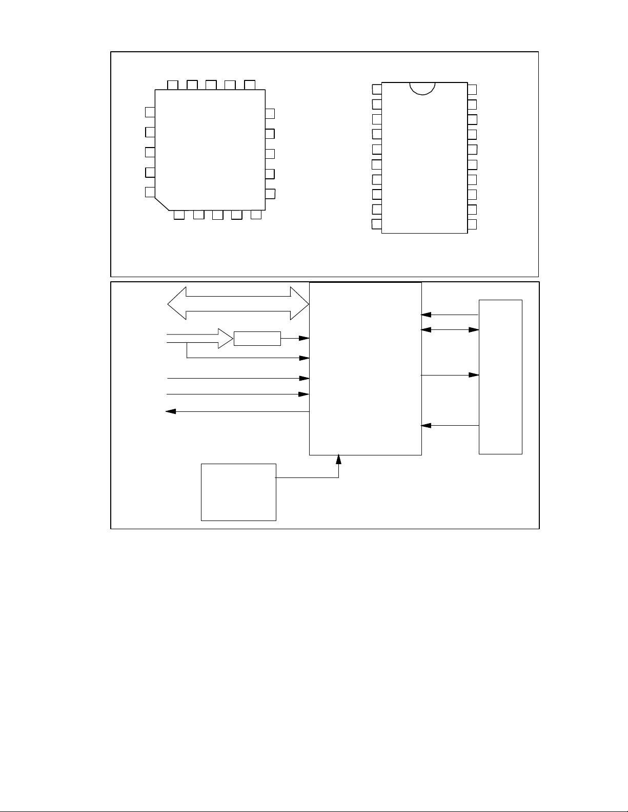
PIN CONFIGURATION
n
C
P
1
TXRXRSn
I
N
T
n
R
D
D
2
D3D
4
n
W
R
Package: 20 Pin PLCC
Package 20 Pin DIP
TTL CLOCK
TTL/RS-232-C
2
nCP
Vcc
0
D
D
1
nCS
DATA BUS
ADDRESS
BUS
nWRITE
nREAD
18 17 16 15 14
19
20
1
2
3
4 5 6 7 8
13
12
11
10
9
DECODE
CLOCK
D
7
D6
GND
D
5
D0-D7
nCS
RS
nWR
nRD
D
0
D1
nCS
nRD
2
D
D3
D4
nWR
D5
GND
10
COM81C17
TWENTY
PIN
UART
1
2
3
4
5
6
7
8
9
nCP1
nCP2
TX
20
19
18
17
16
15
14
13
12
11
Vcc
CP
2
CP
1
TX
RX
RS
nINT
CLOCK
D
7
D
6
INTERRUPT
REQUEST
nINT
RX
5.0688 MHZ
FIGURE 1 – TYPICAL TPUART INTERFACE
OSCILLATOR
OR
FIGURE 1 – TYPICAL TPUART INTERFACE
Page 4
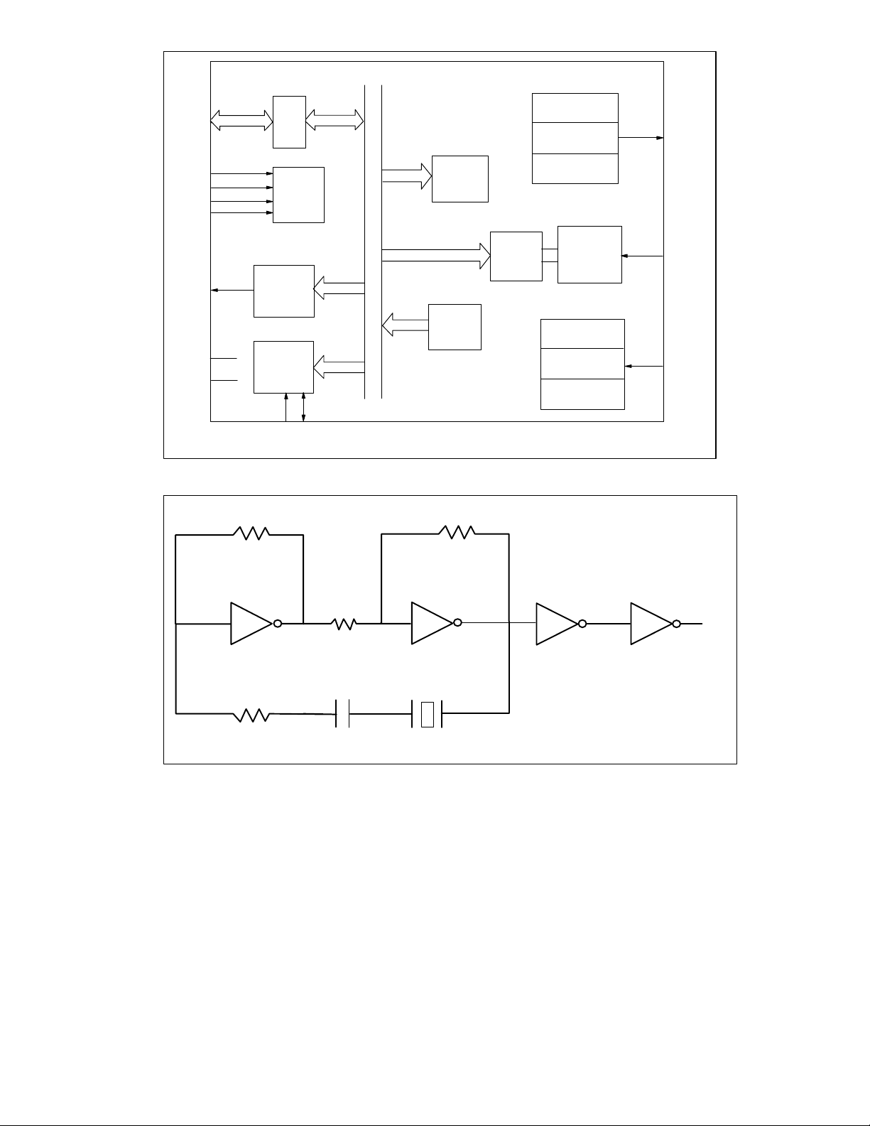
4
D0-D7
n
C
P
1
n
C
P
2
INTERNAL DATA BUS
220 OHM 30 pF 5.0688 MHz
nCS
nRD
nWR
RS
DATA
BUS
TRANS
READ
WRITE
DECODE
LOGIC
MODE
REGISTER
TRANSMIT
BUFFER
TRANSMIT
SHIFT REGISTER
TRANSMIT
CONTROL
TX
nINT
VCC
GND
MASK
REGISTER
& LOGIC
STATUS
REGISTER
CONTROL
REGISTER
FIGURE 2 – COM81C17 BLOCK DIAGRAM
1800 OHM 560 OHM
220 OHM
7404 7404
BAUD
RATE
SELECT
REGISTER
BAUD
RATE
GENERATOR
RECEIVE
CONTROL
RECEIVE
SHIFT REGISTER
RECEIVE
BUFFER
7404 7404
CLOCK
RX
FIGURE 2A – 5.0688 MHz CRYSTAL OSCILLATOR CIRCUIT
Page 5

5
DESCRIPTION OF PIN FUNCTIONS
DIP PIN NO. NAME SYMBOL
1, 2, 5-7,
9,11-12
DATA BUS D0-D7An 8-bit bi-driectional DATA BUS is used to
interface the TPUART to the processor Data Bus.
3 CHIP SELECT nCS A low level on this input enables the TPUART for
reading and writing to the processor. When nCS is
high, the DATA BUS is in high impedance and the
nWR and nRD will have no effect on the chip.
4 READ DATA
STROBE
nRD A low pulse on this input (when nCS is low) enables
the TPUART to place the data or the status
information on the DATA BUS.
8 WRITE DATA
STROBE
nWR A low pulse on this input (when nCS is low) enables
the TPUART to accept the data or control word
from the DATA BUS into the TPUART.
10 GROUND GND Power Supply Return.
13 CLOCK CLK External TTL Clock Input (See Table 2)
14 INTERRUPT
REQUEST
nINT An interrupt request is asserted by the TPUART
when an enabled condition has occurred in the
Status Register. This is an active low, open drain
output. This pin has an internal pullup register.
15 REGISTER
SELECT
RS During processor to TPUART communications, this
input is used to indicate which internal register will
be selected for access by the processor. When this
input is low, data can be written to the TX Holding
Buffer or data can be read from the RX Holding
Register. When this input is high control words can
be written to the Control Register or status
information can be read from the Status Register.
16 RECEIVER DATA RX This input is the receiver serial data. A high to low
transition is required to initiate data reception.
17 TRANSMITTER
DATA
TX This output is the transmitted serial data from the
TPUART. When a transmission is concluded, the
TX line will always return to the mark (High) state.
18 CONTROL PIN 1 nCP1 This control pin is an input only pin. It can be
programmed to perform the functions of CTS or
DSR/DCD.
19 CONTROL PIN 2 nCP2 This control pin can be programmed to be either an
input or an output. When in input mode, this pin
can perform the functions of DSR/DCD. When in
output mode, this pin can perform the functions of
DTR or RTS.
20 POWER SUPPLY V
+5V Supply Voltage
CC
DESCRIPTION
Page 6

6
FUNCTIONAL DESCRIPTION
RESETTING THE TPUART
The TPUART must be reset on power up. Since
there is no external pin allocated for hardware
reset, this is accomplished by writing a One
(HIGH) followed by writing a Zero (LOW) to the
Command Register bit 7. Following reset, the
TPUART enters an idle state in which it can
neither transmit nor receive data.
INITIALIZING THE TPUART
The TPUART is initialized by writing three
control words from the processor. Only a single
address is set aside for Mode, Baud Rate
Select, Interrupt Mask and TX Buffer Registers.
For this to be possible, logic internal to the chip
directs information to its proper destination
based on the sequence in which it was written.
Following internal reset, the first write to address
zero (i.e. RS = 0) is interpreted as a Mode
Control word. The second write is interpreted as
Interrupt Mask word. The third write is
interpreted as Baud Rate Select. The fourth and
all subsequent writes are interpreted as writes to
the TX Buffer Register.
There is one way in which control logic may
return to anticipating a Mode, Interrupt Mask,
and Baud Rate Select words. This is following
an internal reset. Following initialization, the
TPUART is ready to communicate.
PROGRAMMABLE CONTROL PINS
The TPUART provides two programmable
control pins that can be configured to perform
as modem or terminal control handshake
signals. If no handshake signal is required,
these pins can be used as general purpose one
bit Input or Output ports.
nCP1 - is an input only pin that can be
programmed to act as the CTS (Clear To Send)
handshake signal, where it will disable data
transmission by the TPUART after the contents
of the Transmit Shift Register is completely
flushed out. When programmed as 1, nCP1 will
serve as a general purpose 1 bit input port. The
inverted state will be reflected in Status Register
bit 0 (when programmed as CTS or general
purpose input bit).
nCP2 - is an Input/Output pin. When configured
as Output, its state is directly controlled by the
host processor via writes to the Control
Register. This will serve the purpose of modem
and terminal handshake signals as RTS (Reset
To Send), and DTR (Data Terminal Ready).
When configured as Input, its inverted state is
reflected in the Status Register bit 1 and read by
the processor. This will serve the purpose of
handshake signals as DCD (Data Carrier
Detect) and DSR (Data Set Ready).
MODE REGISTER
BIT 1 BIT 2
0 0 nCP2 is RTS Output
0 1 nCP2 is GP Output
1 X nCP2 is GP Input
1 X nCP2 is GP Input
Page 7

7
THE ON CHIP BAUD RATE GENERATOR
Register bit 3 to accept a 16X external clock.
The Baud Rate Generator will not assume any
The TPUART incorporates an on chip Baud
Rate Generator that can be programmed to
generate sixteen of the most popular baud rates.
The TPUART also allows the bypassing of the
given baud rate upon power up, therefore it
must be programmed as desired. The following
chart is based on a 5.0688 MHz CLOCK
frequency.
Baud Rate Generator by programming Mode
Table 2 - 16X CLOCK
Clock Frequency = 5.0688 MHz
Baud Rate
Select Register
D3D2D1D
Theoretical
Baud
Rate
0
Frequency
16X Clock
Actual
Frequency
16X Clock
Percent
Error
Duty
Cycle % Divisor
0 0 0 0 50 0.8 kHz 0.8 kHz 50/50 6336
0 0 0 1 110 1.76 1.76 50/50 2880
0 0 1 0 134.5 2.152 2.1523 0.016 50/50 2356
0 0 1 1 150 2.4 2.4 50/50 2112
0 1 0 0 300 4.8 4.8 50/50 1056
0 1 0 1 600 9.6 9.6 50/50 528
0 1 1 0 1200 19.2 19.2 50/50 264
0 1 1 1 1800 28.8 28.8 50/50 176
1 0 0 0 2000 32.0 32.081 0.253 50/50 158
1 0 0 1 2400 38.4 38.4 50/50 132
1 0 1 0 3600 57.6 57.6 50/50 88
1 0 1 1 4800 76.8 76.8 50/50 66
1 1 0 0 7200 115.2 115.2 50/50 44
1 1 0 1 9600 153.6 153.6 48/52 33
1 1 1 0 19.200 307.2 316.8 3.125 50/50 16
1 1 1 1 38.400 614.4 633.6 3.125 50/50 8
Page 8

8
REGISTER DESCRIPTIONS
CP1
CP2 I/O
- The Mode Register bit 1 determines whether the CP2 pin will be configured as a
Status Register bit 1. When used as an output, it’s state is controlled by the processor via
CP2
CLOCK SELECT
PARITY ENABLE
PARITY
NUMBER OF DATA BITS
Table 3 - COM81C17 Mode Register Description (Bits 0 - 7)
BIT DESCRIPTION
0
- The Mode Register bit 0 determines whether the CP1 pin will be configured to provide
the function of CTS or will serve as a general purpose 1 bit input port. In either case, its
state will be reflected in Status Register bit 0.
0 → nCP1 = CTS
1 → nCP1 = GP INPUT
1
general purpose 1 bit output port or will serve as a general
purpose 1 bit input port. When used as an input, its state is reflected in the
the Control Register bit 1.
0 → nCP2 = OUTPUT
1 → nCP2 = INPUT
2
- The mode register bit 2 determines whether the nCP2 pin will be configured to provide
the function of RTS or will serve as a general purpose 1 bit output port.
0 → nCP2 = RTS
1 → nCP2 = GP OUTPUT
3
- The Mode Register bit 3 determines whether the internal Baud Rate
Generator will supply the TX and RX clocks or the clock on the clock pin will be used as a
16X clock. The Baud Rate Select Register contents will be bypassed when an external 16X
clock is used.
0 = INTERNAL CLOCK
1 = EXTERNAL CLOCK (16X)
4
- The Mode Register bit 4 determines whether parity generation and
checking will be enabled.
0 = PARITY DISABLE
1 = PARITY ENABLE
5
- The Mode Register bit 5 determines whether odd or even parity will be generated
and checked.
0 = EVEN PARITY
1 = ODD PARITY
6
- The Mode Register bit 6 determines the number of data bit that
will be presented in each data character (i.e. 7 or 8)
0 = 7BITS PER CHARACTER
1 = 8 BITS PER CHARACTER
7
STOP BITS
- The Mode Register bit 7 determines how many stop bits will trail
each data unit (i.e. 1 or 2)
0 = 1 STOP BIT
1 = 2 STOP BITS
A data frame will consist of a start bit, 7 or 8 data bits, an optional parity bit, and 1 or 2 stop
bits.
Page 9

9
Table 4 - COM81C17 Status Registers Description (Bits 0-7)
CP2
TX SHIFT REGISTER EMPTY
PARITY ERROR
OVERRUN ERROR
FRAMING ERROR
TX BUFFER EMPTY
BIT DESCRIPTION
0
1
- This reflects the inverted state of the control pin CP1.
CP1
- This is active only when the nCP2 pin is programmed be to an input. It is set by its
corresponding input pin and reflects the inverted state of the control pin nCP2. When the
CP2 pin is programmed as an output, this bit is forced to a zero.
2
- This signals the processor that the Transmit Shift
Register is empty. A typical program will usually load the last character of a transmission
and then monitor the TX SHIFT REGISTER EMPTY bit to determine when it is a safe
time for disabling transmission. This bit is set when the Transmitter Shift Register has
completed transmission of a character, and no new character has been loaded in the
Transmit Buffer Register. This bit is also set by asserting internal reset. This bit is
cleared by:
A) Loading the TX Buffer Register
3
- This signals the processor that the character stored in the Receive
Character Buffer was received with an incorrect number of binary "1" bits. This bit is set
when the received character in the Receiver Buffer Register has an incorrect parity bit and
parity has been enabled. This bit is cleared by:
A) Setting Reset Errors in the Control Register
B) Asserting internal reset
4
- This is set whenever a byte stored in the Receive Character Buffer
is overwritten with a new byte from the Receive Shift Register before being transferred to
the processor. This bit is cleared by:
A) Setting Reset Errors in the Control Register
B) Asserting internal reset
5
- This is set whenever a byte in the Receive Character Buffer was
received with an incorrect bit format ("0" stop bits). This bit is cleared by:
A) Setting Reset Errors in the Control Register
B) Asserting internal reset
6
- This signals the processor that the Transmit Buffer Register is
empty and that the TPUART can accept a new character for transmission. This bit is set
when:
A) A character has been loaded from the Transmit Buffer Register to the Transmit
Shift Register
B) Asserting the TRANSMIT RESET bit in the Control Register
C) Asserting internal reset
This bit is cleared by:
A) Writing to the Transmit Buffer Register
This bit is initially set when the transmitter logic is enabled by setting the TX Enable bit in
the Control Register (also TX Buffer is empty because of reset). Data can be overwritten
if a consecutive write is performed while TX Buffer Empty is zero.
Page 10

10
BIT DESCRIPTION
RX BUFFER FULL
CP2
RX ENABLE
TX ENABLE
RESET ERRORS
INTERNAL RESET
7
- This signals the processor that a completed character is present in
the Receive Buffer Register for transfer to the processor. This bit is set when a character
has been loaded from the receive deserialization logic to the Receive Buffer Register.
This bit is cleared by:
A) Reading the Receive Buffer Register
B) Asserting the RECEIVER RESET bit in the Control Register
C) Asserting internal reset
Table 5 – COM81C17 CONTROL REGISTER DESCRIPTION (BITS 0-7)
BIT DESCRIPTION
0 Not used (test mode bit, must be zero).
1
– This bit controls the nCP2 output pin. Data at the output is the logical
compliment of the register data. When the CP2 bit is set, the nCP2 pin is forced low.
When CP2 is RTS, a 1 to 0 transition of the CP2 bit will cause the nCP2 pin to go high
one TXc time after the last serial bit has been transmitted.
2
– This bit when reset will disable the setting of the RX BUFFER FULL bit
in the Status Register which informs the processor of the availability of a received
character in the Receive Buffer Register. The error bits in the Status Register will be
cleared and will remain cleared when RX is disabled.
3
4
RX RESET
TX RESET
5
– This will reset the receiver block only.
– This will reset the transmitter block only.
– Data transmission cannot take place by the TPUART unless this bit is
set. When this bit is reset (disable), transmission will be disabled only after the
previously written data has been transmitted.
6
– This bit when set will reset the parity, overrun, and framing error
bits in the Status Register. No latch is provided in the Control Register for saving this
bit; therefore there is no need to clear it (error reset = d6.RS.nWR).
7
– This bit enables the resetting of the internal circuitry and initializes
access to address 0 to be sequential.
Page 11

11
INTERRUPT MASK REGISTER DESCRIPTION
REGISTER DECODE & TRUTH TABLE
This is an eight bit write only register which is
loaded by the processor. These bits are used to
enable interrupts from the corresponding bits in
the Status Register. This register is reset with
internal reset.
Table 6 - DECODE TRUTH TABLE
RS nRD nWR nCS
0 0 1 0 READ RX BUFFER REGISTER
0 1 0 0 WRITE TO TX BUFFER
1 0 1 0 READ STATUS REGISTER
1 1 0 0 WRITE TO CONTROL
X X X 1 DATA BUS IN TRI STATE
The first write to address zero (RS = 0) will
access the Mode Register, the second will
access the Interrupt Mask Register, the third will
access the Baud Rate Select Register, the fourth
and all subsequent writes will access the TX
Buffer Register.
The TPUART provides unique decode capability
to three of the seven internal processor
accessible register. These are the RX Buffer
Register (read only), the Status Register (read
only) and the Control Register (write only). The
other four registers (write only) are decoded in a
sequential manner following reset. Refer to
table below:
REGISTER
REGISTER
Following reset, the decode sequence of writes
to address 0 is as follows:
RS0 - Selects the Mode Control Register
RS1 - Selects the Interrupt Mask Register
RS2 - Selects the Baud Rate Select Register
RS3 - Selects the TX Buffer Register
Table 7 - INTERNAL REGISTER SELECT
RS0 RS1 RS2 RS3
0 1 1 1 AFTER RESET
1 0 1 1 AFTER FIRST WRITE
1 1 0 1 AFTER SECOND WRITE
1 1 1 0 AFTER THIRD WRITE
1 1 1 0 ALL SUBSEQUENT
WRITES
Page 12

12
OPERATIONAL DESCRIPTION
MAXIMUM GUARANTEED RATINGS*
Operating Temperature Range
Storage Temperature Range
.........................................................................................
..........................................................................................
Lead Temperature Range (soldering, 10 seconds)
Positive Voltage on any pin
.....................................................................................................
Negative Voltage on any pin, with respect to ground
Maximum V
CC
................................................................................................................................
....................................................................
...................................................................
0oC to +70oC
-55o to +150oC
+325oC
Vcc+0.3V
-0.3V
+7V
*Stresses above those listed above could cause permanent damage to the device. This is a stress
rating only and functional operation of the device at any other condition above those indicated in the
operation sections of this specification is not implied.
Note: When powering this device from laboratory or system power supplies, it is important that the
Absolute Maximum Ratings not be exceeded or device failure can result. Some power supplies exhibit
voltage spikes on their outputs when the AC power is switched on or off. In addition, voltage
transients on the AC power line may appear on the DC output. If this possibility exists, it is suggested
that a clamp circuit be used.
Table 8 - ELECTRICAL CHARACTERISTICS
T = 0oC to +70oC, VCC = +5.0V ± 5%
PARAMETER SYMBOL
LOW INPUT VOLTAGE
HIGH INPUT VOLTAGE
LOW OUTPUT VOLTAGE
V
V
IH
V
OL
MIN TYP MAX UNITS
IL
2.0
0.8
0.4
V
V
V
IOL = 5.0ma D0 - D
COMMENTS
7
IOL = 3.5ma
HIGH OUTPUT VOLTAGE
INPUT LEAKAGE CURRENT
INPUT CAPACITANCE
POWER SUPPLY CURRENT
V
OH
I
L
C
IN
I
CC
2.4
10
15
±10
V
µA
pF
ma
IOH = 100µa
Page 13

13
Table 9 - AC CHARACTERISTICS
SYMBOL DESCRIPTION MIN TYP MAX UNITS
AC CHARACTERISTICS
WRITE CYCLE
t
1
t
2
t
3
t
4
t
5
READ CYCLE
t
6
t
7
t
8
t
9
t
10
nCS, RS to nWR ↓ setup time
nCS, RS hold time to nWR
↑
nWR pulse width
Data BUS in setup time to nWR
Data BUS in hold time to nWR
nCS, RS to nWR ↓ setup time
nCS, RS hold time to nWR
↑
nWR pulse width
Data BUS in setup time to nWR
Data BUS in hold time to nWR
50
0
100
75
↑
10
↑
50
0
100
0
0
↑
60
60
↑
GENERAL TIMING
t
11
t
12
t
13
t
14
t
15
Reset Pulse Width
nCP1 active to nINT
nWR rising edge to nCP2 change
CP1, CP2 pulse width
Read Write Interval
1.0
300
200
1.0
100
nCP1, nCP2 data
Rise Time
3030ns @25pf
Fall Time
CLOCK FREQUENCY
Rise Time
Fall Time
Internal Baud Rate Mode
External Baud Rate Mode
Duty Cycle
30
30
11.0
1.6
40/60
ns
ns
ns
ns
ns
ns
ns
ns
ns @50pf max
ns @50pf max
s
µ
s @25pf
µ
s
µ
s
µ
ns
ns @25pf
ns
ns
MHz
MHz
%
Page 14

14
nCS
RS
nWR
D
nCS
1
t
t3
t4
IN
t2
15
t
t5
FIGURE 3 – PROCESSOR TO TPUART WRITE CYCLE
nRD
OUT
D
RS
t6
t8
t9
t7
15
t
t10
valid data
FIGURE 4 – PROCESSOR FROM TPUART READ CYCLE
Page 15

15
nWR
RESET
TO CONTROL
REGISTER
D
7IN
INTERNAL
nCP1
nCP2
nINT
t11
FIGURE 5 – INTERNAL RESET TIMING
t
12
FIGURE 6 – nCP1 TRANSITION TO nINT
Page 16

16
nWR
nCP2
nCP1
nCP2
t13
FIGURE 7 – nCP2 OUTPUT TIMING
t14
FIGURE 8 – nCP1, nCP2 INPUT TIMING
Page 17

17
Page 18

8
1988 STANDARD MICROSYSTEMS
CORP.
Circuit diagrams utilizing SMSC products are included as a means of illustrating typical
applications; consequently complete information sufficient for construction purposes is
not necessarily given. The information has been carefully checked and is believed to be
entirely reliable. However, no responsibility is assumed for inaccuracies. Furthermore,
such information does not convey to the purchaser of the semiconductor devices
described any licenses under the patent rights of SMSC or others. SMSC reserves the
right to make changes at any time in order to improve design and supply the best
product possible. SMSC products are not designed, intended, authorized or warranted
for use in any life support or other application where product failure could cause or
contribute to personal injury or severe property damage. Any and all such uses without
prior written approval of an Officer of SMSC and further testing and/or modification will
be fully at the risk of the customer.
 Loading...