

Page 1

)
)
.
.
CNY17 SERIES
TRIOS“ PHOTOTRANSISTOR
OPTOCOUPLER
FEATURES
• High Current Transfer Ratio
CNY17-1, 40 to 80%
CNY17-2, 63 to 125%
CNY17-3, 100 to 200%
CNY17-4, 160 to 320%
• Breakdown V oltage, 5300 VA C
RMS
• Field-Effect Stable by TRIOS*
• Long Term Stability
• Industry Standard Dual-in-Line Package
• Underwriters Lab File #E52744
V
• VDE #0884, Available with Option 1
DE
DESCRIPTION
The CNY17 is an optically coupled pair consisting
of a Gallium Arsenide infrared emitting diode optically coupled to a silicon NPN phototransistor.
Signal information, including a DC level, can be
transmitted by the device while maintaining a high
degree of electrical isolation between input and output.
Dimensions in inches (mm)
3
248 (6.30)
256 (6.50)
4
5
.335 (8.50)
.343 (8.70)
.039
(1.00)
Min.
4°
typ.
.018 (0.45)
.022 (0.55)
Pin One ID
12
6
.130 (3.30)
.150 (3.81)
.020 (.051) min.
.031 (0.80)
.035 (0.90)
.100 (2.54) typ.
Anode
Cathode
NC
1
2
3
.300 (7.62)
18° typ.
.010 (.25)
.014 (.35)
.300 (7.62)
.347 (8.82)
typ.
6
Base
5
Collector
4
Emitter
.110 (2.79
.150 (3.81
The CNY17 can be used to replace relays and
transformers in many digital interface applications,
as well as analog applications such as CRT modu-
Characteristics
(T
A
=25°C)
Symbol Unit Condition
lation.
Maximum Ratings
(TA=25°C)
Emitter
Reverse Voltage.................................................6 V
Forward Current............................................ 60 mA
Surge Current (t
≤
10µs)................................... 2.5 A
Power Dissipation.......................................100 mW
Detector
Collector-Emitter Breakdown Voltage...............70 V
Emitter-Base Breakdown Voltage.......................7 V
Collector Current.......................................... 50 mA
Emitter
Forward Voltage V
Breakdown Voltage V
Reverse Current I
Capacitance 25 pF VR = 0 V, f =1 MHz
Thermal Resistance R
Detector
F
BR
R
thjamb
1.25
(≤1.65)
6VI
≥
0.01 (≤10)µAVR = 6 V
750 K/W
VI
= 60 mA
F
= 10 mA
R
Collector Current (t <1 ms)......................... 100 mA
Power Dissipation.......................................150 mW
Capacitance C
Package
Isolation Test V oltage (Between emitter &
detector referred to climate DIN 40046,
part 2, Nov. 74)..............................5300 VAC
Creepage Distance
Clearance Distance
.......................................... ≥
......................................... ≥
RMS
7 mm
7 mm
Isolation Thickness between
Emitter and Detector
Comparative Tracking Index per DIN IEC 112/
.................................≥
0.4 mm
Thermal Resistance R
Package
Collector-Emitter
Saturation Voltage V
Coupling Capacitance C
CE
C
CB
C
EB
thjamb
CEsat
C
5.2
6.5
7.5
500 K/W
0.25 (≤0.4) V
0.6 pF
pF
pF
pF
VCE =5 V, f =1 MHz
VCB =5 V, f =1 MHz
VEB =5 V, f =1 MHz
IF =10 mA,
IC=2.5 mA
VDE0303, part 1.............................................175
Isolation Resistance
V
=500 V, TA=25°C
IO
VIO=500 V, TA=100°C
...................................≥
................................≥
1012
1011
Ω
Ω
Storage Temperature................... –55°C to +150°C
Operating Temperature............... –55
Junction Temperature....................................100
°
C to +100°C
°
C
Soldering Temperature (max . 10 s, dip soldering:
distance to seating plane
≥
1.5 mm)..........260°C
5–1
This document was created with FrameMaker 4.0.4
Page 2

Current Transfer Ratio and Collector-Emitter Leakage Current
V
V
by dash number
IC/IF at VCE=5 V
(IF=10 mA) 40-80 63-
IC/IF at VCE=5 V
(IF=1 mA) 30
Collector-Emitter
Leakage Current
(VCE=10 V)
(I
)
CEO
(T
=25°C)
A
-1 -2 -3 -4 Unit
(>13)
2 (≤
50)
125
45
(>22)
2 (≤
50)
100200
70
(>34)
5 (≤
100)
160320
90
(>56)
5 (≤
100)
%
%
nA
Figure 3. Current transfer ratio versus
diode current
(T
=–25°C, VCE=5 V)
A
IC/IF=f (IF)
Figure 1. Linear Operation
I
F
(without saturation)
RL=75 Ω
I
C
47 Ω
=10 mA, VCC=5 V, TA=25 °C
I
F
Load Resistance R
Turn-On Time t
Rise Time t
Turn-Off Time t
Fall Time t
Cut-off Frequency f
L
ON
R
OFF
f
CO
Figure 2. Switching Operation
I
F
1 KΩ
V
=5
CC
75
3.0
2.0
2.3
2.0
250 kHz
(with saturation)
=5
V
CC
Figure 4. Current transfer ratio versus
diode current
I
=f (IF)
C/IF
Ω
µ
s
µ
s
µ
s
µ
s
(T
A
=0°C, V
CE
=5 V)
47 Ω
Turn-On Time t
Rise Time t
Turn-Off Time t
Fall Time t
-1
(I
=20 mA)
F
3.0 4.2 6.0
ON
2.0 3.0 4.6
R
18 23 25
OFF
11 14 15
F
-2 and -3
(IF=10 mA)-4(IF=5 mA)
µ
µ
µ
µ
5–2
Figure 5. Current transfer ratio versus
diode current (T
I
=f (IF)
C/IF
s
s
s
s
=25°C, VCE=5 V)
A
Page 3
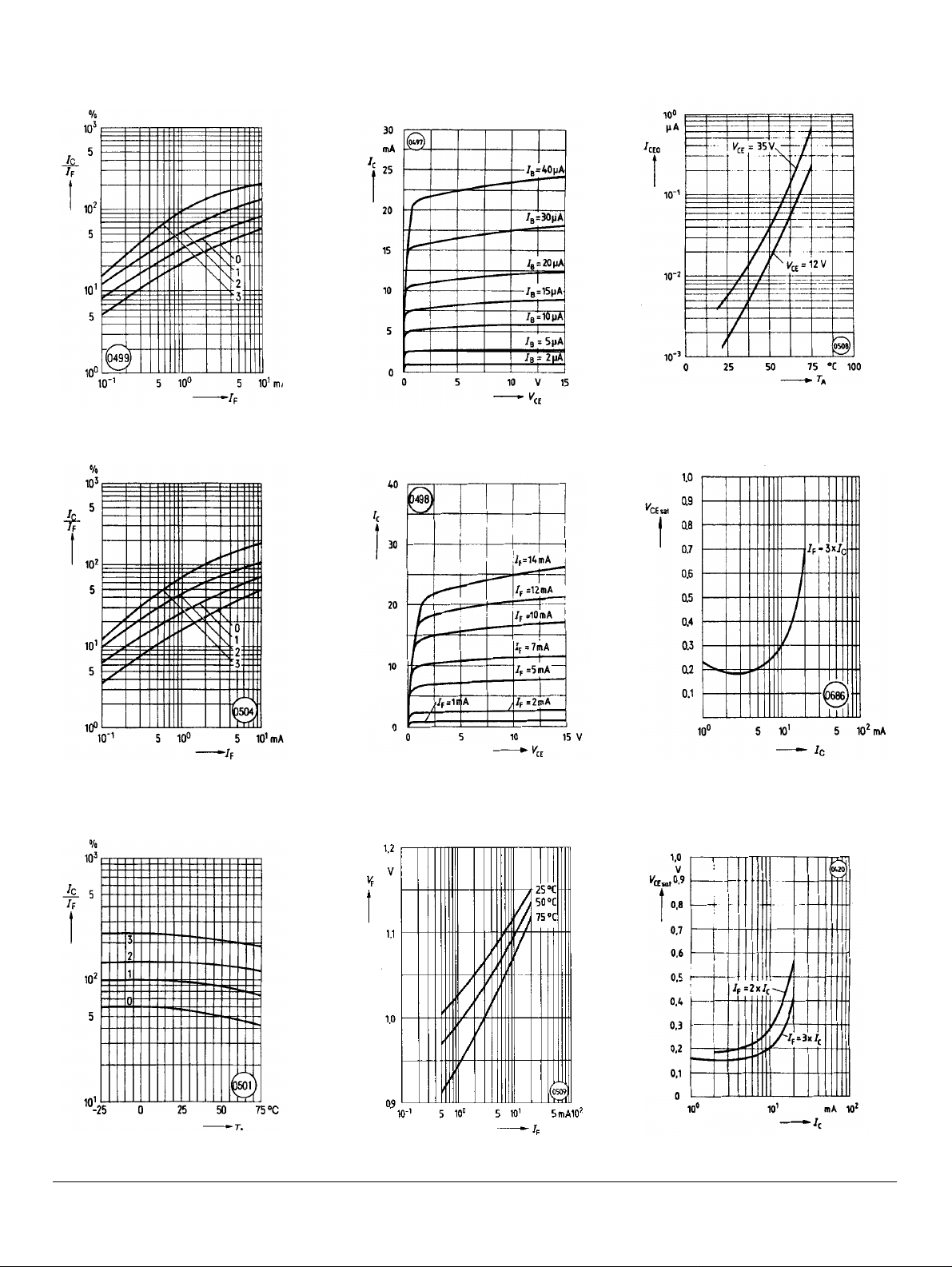
Figure 6. Current transfer ratio versus
diode current (T
V
=5 V, IC/IF=f (IF)
CE
=50°C)
A
Figure 7. Current transfer ratio versus
diode current (T
=75°C) VCE=5 V
A
Figure 9. Transistor characteristics
(B=550) CNY17-3, -4 I
(T
=25°C, IF=0)
A
=f(VCE)
C
Figure 10. Output characteristics
CNY17-3, -4 (T
=25°C) IC=f(VCE)
A
Figure 12. Collector emitter off-state
current I
=f (V, T) (TA=25°C, IF=0)
CEO
Figure 13. Saturation voltage versus
collector current and modulation
depth CNY17-1 V
=f (IC) (TA=25°C)
CEsat
Figure 8. Current transfer ratio versus
temperature (IF=10 mA, VCE=5 V)
I
=f (T)
C/IF
Figure 11. Forward voltage V
5–3
=f (IF)
F
Figure 14. Saturation voltage versus
collector current and modulation
depth CNY17-2 V
(T
=25°C )
A
CEsat
=f (IC)
Page 4
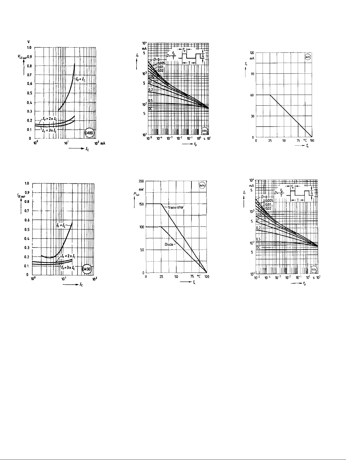
Figure 15. Saturation voltage versus
collector current and modulation
depth CNY17-3 V
=f (IC) (TA=25°C)
CEsat
Figure 17. Permissible pulse load
D=parameter, T
=25°C, IF=f (tp)
A
Figure 19. Permissible forward current P
=f (TA)
tot
Figure 16. Saturation voltage versus
collector current and modulation
depth CNY17-4 V
=f (IC) (TA=25°C)
CEsat
Figure 18. Permissible power dissipation transistor and diode
P
=f (TA)
tot
Figure 20. Transistor capacitance
C=f(V
) (TA=25°C, f=1 MHz)
O
5–4
 Loading...