

0.5-11.5 GHz Divide by 4 Static Prescaler
GaAs Monolithic Microwave IC
Description
The CND2050 is a low power consumption
and very high speed divider by 4
manufactured with a 0.6µm GaAs self
aligned implanted MESFET process.
The design is full differential input/output
that allows direct drive into 50Ω load.
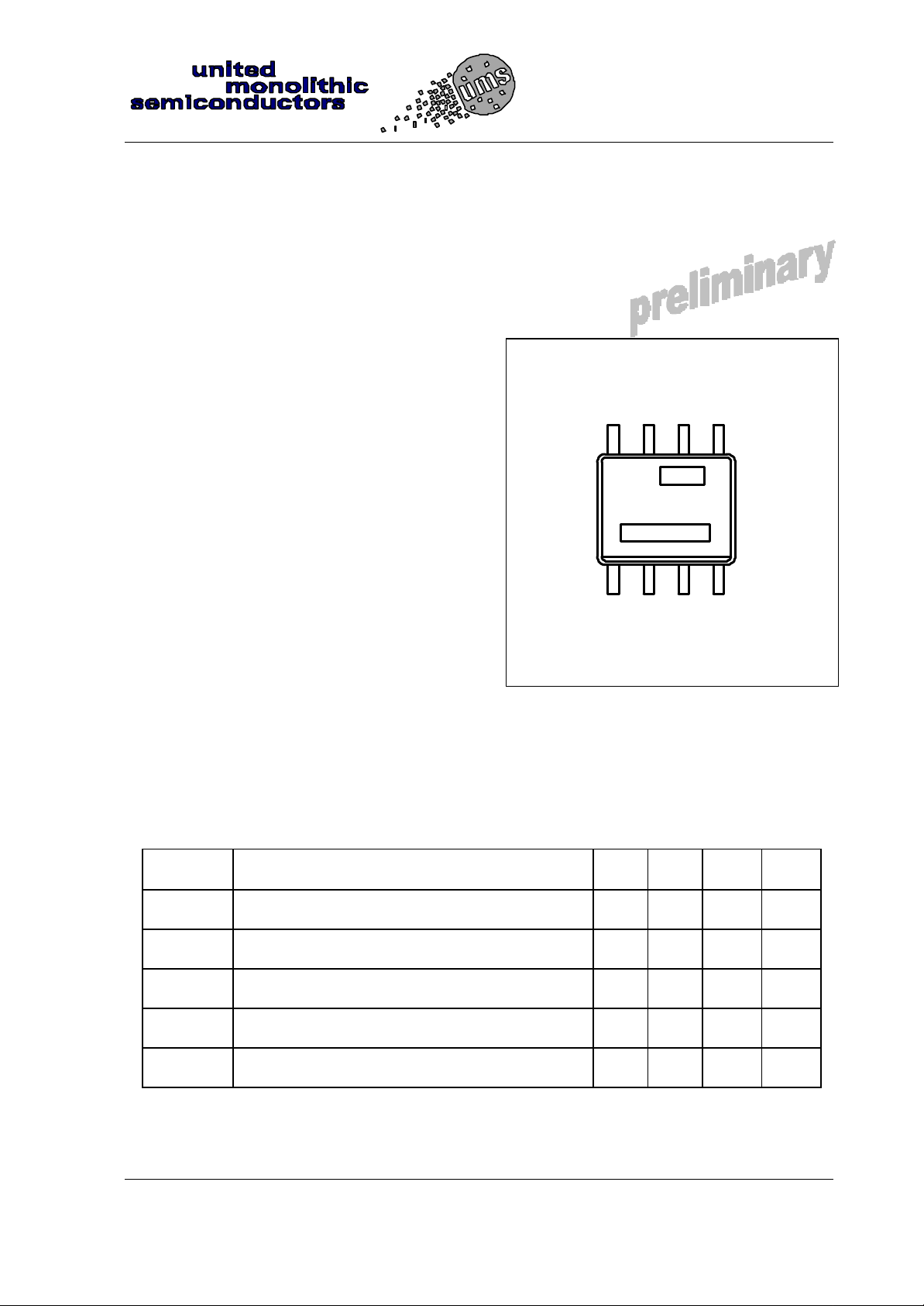
The CND2050 is available in SOIC8
package form .
CND2050
UMS
CND2050
Main Features
Very broad operating frequency range
Low power dissipation: 250mW
Single supply operation:+ 5V or –5V
High input sensitivity:
-10dBm@10 GHz at 25°C
Low phase noise: -139dBc/Hz at 1KHz
SOIC8 plastic package
Main Characteristics
at Tamb= +25°C
Symbol Parameter Min Typ Max Unit
Vdd Bias supply (with Vss = 0) 3.3 5 6 V
Vss Bias supply (with Vdd = 0) -6 -5 -3.3 V
Pdiss Power dissipation 90 250 350 mW
Fmin Minimum input frequency 0.5 GHz
Fmax Maximum input frequency (Vdd=5V) 10 12 GHz
ESD Protections: Electrostatic discharge sensitive device. Observe handling precautions!
Ref. : DSCND20500257 -13-Sep.-00 1/9 Specifications subject to change without notice
United Monolithic Semiconductors S.A.S.
Route Départementale 128 - B.P.46 - 91401 Orsay Cedex France
Tel. : +33 (0)1 69 33 03 08 - Fax : +33 (0)1 69 33 03 09
CND2050
0.5-10GHz frequency divider by 4
Electrical Characteristics (1)
Guaranteed electrical specifications at +25°C
Tested under configuration described in Fig.1 and Fig.2
Vdd = 5V , Vss = 0 ; Pin = 0 dBm ; Zo = 50 Ω
Symbol Parameter Min Typ Max Unit
Fmin Minimum input frequency
(Differential or single input)
Fmax Maximum input frequency
differential input
single input
Pout Minimum output power
(Differential or single input) -5 -2 dBm
Guaranteed electrical specifications at +25°C
Tested under configuration described in Fig.1
Differential inputs ; Vss = 0 ; Pin = 0 dBm ; Zo = 50 Ω
Symbol Parameter Min Typ Max Unit
Fmin Minimum input frequency
Vdd = 3.3 to 5 V 0.5 GHz
10
9
12
11
0.5 GHz
GHz
GHz
Fmax Maximum input frequency
Vdd = 5V
Vdd = 3.3V
Pout Minimum output power
Vdd = 5V
Vdd =3.3V
Ref. : DSCND20500257 -13-Sep.-00 2/9 Specifications subject to change without notice
United Monolithic Semiconductors S.A.S.
Route Départementale 128 - B.P.46 - 91401 Orsay Cedex France
Tel. : +33 (0)1 69 33 03 08 - Fax : +33 (0)1 69 33 03 09
10
9
-5
-10
12
11
-2
-7
GHz
GHz
dBm
dBm
0.5-11.5 GHz Divide by 4 prescaler
CND2050
Electrical Characteristics (2)
Guaranteed electrical specifications over the temperature range of -40°C to +85°C
Tested under configuration described in Fig.1
Differential inputs ; Vss = 0 ; Pin = 0 dBm ; Zo = 50 Ω
Symbol Parameter Min Typ Max Unit
Fmin Minimum input frequency
Vdd = 3.3 to 5 V 0.5 GHz
Fmax Maximum input frequency
Vdd = 5V
Vdd = 3.3V
Pout Minimum output power
Vdd = 5V
Vdd =3.3V
Guaranteed electrical specifications over the temperature range of -40°C to +85°C
Single or differential inputs ; Vss = 0 ; Zo = 50 Ω
Symbol Parameter Min Typ Max Unit
Pin max Maximum operational input power
Vdd = 3.3 to 5 V 10 dBm
9
8
-6
-11
11
10
-3
-8
GHz
GHz
dBm
dBm
Idd Supply current
Vdd= 5V
Vdd=3.3V
Hr Harmonic rejection (ouput signal) 10 dBc
Ref. : DSCND20500257 -13-Sep.-00 3/9 Specifications subject to change without notice
Route Départementale 128 , B.P.46 - 91401 ORSAY Cedex - FRANCE
Tel.: +33 (0)1 69 33 03 08 - Fax : +33 (0)1 69 33 03 09
35
20
45
25
70
40
mA
mA

CND2050
Absolute Maximum Ratings (1)
Tamb= 25°C
Symbol Parameter Values Units
Vdd Drain voltage 7 V
Pin Maximum input power (2) 15 dBm
0.5-11.5 GHz Divide by 4 prescaler
Top
Operating temperature range -40 to +85
Tstg Storage temperature range -65 to +175 °C
(1) Operation of this device above anyone of these parameters may cause permanent damage
(2) Duration <1s.
Typical Characteristics (1)
Typical input power versus frequency
20
Pin max
Vdd=3,3V
-10
10
0
RECOMMENDED OPERATIONAL RANGE AT Vdd=5V
°C
Vdd=5V
Pin (dBm)
-20
-30
-40
-50
0 1 2 3 4 5 6 7 8 9 10 11 12 13 14
Pin min
Frequency (GHz)
Tamb= 25°C, Zo=50Ω, Vdd=5V or 3.3V ; Vss = 0 ; differential inputs
Ref. : DSCND20500257 -13-Sep.-00 4/9 Specifications subject to change without notice
Route Départementale 128 , B.P.46 - 91401 ORSAY Cedex - FRANCE
Tel.: +33 (0)1 69 33 03 08 - Fax : +33 (0)1 69 33 03 09

0.5-11.5 GHz Divide by 4 prescaler
Pin min (dBm)
Pin (dBm)
max
Typical Characteristics (2)
Typical input power versus frequency
5
0
-5
-10
-15
-20
-25
-30
CND2050
single input
differential inputs
-35
-40
0 1 2 3 4 5 6 7 8 9 10 11 12 13 14
Frequency (GHz)
Tamb= 25°C, Zo=50Ω, Vdd=5V ; Vss = 0 ; differential inputs or single input
20
10
+85°C +25°C
0
-10
-20
min
-30
- 40°C
-40
-50
0 1 2 3 4 5 6 7 8 9 10 11 12 13 14
Frequency (GHz)
Tamb= -40 to +85°C, Zo=50Ω, Vdd=5V ; Vss = 0 ; differential inputs
Ref. : DSCND20500257 -13-Sep.-00 5/9 Specifications subject to change without notice
Route Départementale 128 , B.P.46 - 91401 ORSAY Cedex - FRANCE
Tel.: +33 (0)1 69 33 03 08 - Fax : +33 (0)1 69 33 03 09

CND2050
Pout (dBm)
0.5-11.5 GHz Divide by 4 prescaler
Typical Characteristics (3)
Output power versus frequency Bias current versus Vdd
0
Vdd=5V
-2
-4
-6
Vdd=3,3V
-8
-10
0 1 2 3 4 5 6 7 8 9 10 11 12 13 14
F (GHz)
60
50
40
Idd (mA)
30
20
3 4 5 6
Tamb= 25°C, Zo=50Ω, Vdd=5V or 3.3V ; Vss = 0 ; differential inputs or single input
SSB Phase noise versus Offset Frequency (Fin=4GHz)
Vdd (V)
0
-20
-40
-60
-80
-100
-120
SSB phase noise (dBc/Hz)
-140
-160
10 100 1000 10000 100000
Offset frequency (Hz)
Ref. : DSCND20500257 -13-Sep.-00 6/9 Specifications subject to change without notice
Route Départementale 128 , B.P.46 - 91401 ORSAY Cedex - FRANCE
Tel.: +33 (0)1 69 33 03 08 - Fax : +33 (0)1 69 33 03 09

0.5-11.5 GHz Divide by 4 prescaler
Signal
generator
50 Ohms
load
Tansmission lines
are 50 Ohms
1
nF1 nF
Q
Vdd
QB
50 Ohms
1
nF
Vss
Vss
50 Ohms
load
Tansmission lines
are 50 Ohms
Spectrum
analyzer
50 Ohms
load1 nF1 nF1 nF1 nF
0¦
Vdd
Vss
Vss
Typical bias tuning
CND2050
1
Signal generator
180°¦
4
8
5
Fig.1 : Typical measurement and RF biasing configuration with differential inputs
1 nF
1
8
F/4 RF output (50 Ohms)
CK
CKB
4
5
Fig.2 : RF biasing configuration with single input and ouput
Vdd Vdd
Internal divider by 4
5K
Vss
5K
Fig.3 : Chip block diagram
500
500
Vss
Q
QB
Ref. : DSCND20500257 -13-Sep.-00 7/9 Specifications subject to change without notice
Route Départementale 128 , B.P.46 - 91401 ORSAY Cedex - FRANCE
Tel.: +33 (0)1 69 33 03 08 - Fax : +33 (0)1 69 33 03 09

CND2050
5+/-0.15
[0.20+/-0.006]
3.81
[.15]
1.27
[0.05]
0.4
[.015]8° max
1.7
max
1.4
[0.055]
0.1+/-0.15
[.004+/-.006]
0.2
[0.006]
Unit: mm [In]
General tolerance
: +/-0.05 [+/-.002]
[0.067]
CND2050
SOIC8 Mechanical Data
8 5
UMS
6+/-0.15
[.236+/-.006]
0.5-11.5 GHz Divide by 4 prescaler
3.7
[.145]
Ordering Information
1
4
Pin out Signal
1 Vdd
2 CK
3 CKB
4 Vss
5 Vss
6 QB
7 Q
8 Vdd
SOIC8 Package : CND2050-DAF/20
Information furnished is believed to be accurate and reliable. However United Monolithic Semiconductors
S.A.S. assumes no responsibility for the consequences of use of such information nor for any infringement of
patents or other rights of third parties which may result from its use. No license is granted by implication or
otherwise under any patent or patent rights of United Monolithic Semiconductors S.A.S.. Specifications
mentioned in this publication are subject to change without notice. This publication supersedes and replaces
all information previously supplied. United Monolithic Semiconductors S.A.S. products are not authorised for
use as critical components in life support devices or systems without express written approval from United
Ref. : DSCND20500257 -13-Sep.-00 8/9 Specifications subject to change without notice
Route Départementale 128 , B.P.46 - 91401 ORSAY Cedex - FRANCE
Tel.: +33 (0)1 69 33 03 08 - Fax : +33 (0)1 69 33 03 09

0.5-11.5 GHz Divide by 4 prescaler
Monolithic Semiconductors S.A.S.
CND2050
Ref. : DSCND20500257 -13-Sep.-00 9/9 Specifications subject to change without notice
Route Départementale 128 , B.P.46 - 91401 ORSAY Cedex - FRANCE
Tel.: +33 (0)1 69 33 03 08 - Fax : +33 (0)1 69 33 03 09
 Loading...