

Page 1
Advance Information
This document contains information on a product under development. The parametric information
contains target parameters that are subject to change.
CN8478/CN8474A/CN8472A/CN8471A
Multichannel Synchronous Communications Controller (MUSYCC™)
Product Description
The CN8478, CN8474A, CN8472A, and CN8471A are advanced Multichannel
Synchronous Communication Controllers (MUSYCCs) that format and deformat up
to 256 (CN8478), 128 (CN8474A), 64 (CN8472A), or 32 (CN8471A) HDLC
channels in a single CMOS integrated circuit. MUSYCC operates at Layer 2 of the
Open Systems Interconnection (OSI) protocol reference model. MUSYCC provides
a comprehensive, high-density solution for processing HDLC channels for
internetworking applications such as Frame Relay, ISDN D-channel signaling,
X.25, Signaling System 7 (SS7), DXI, ISUP, and LAN/WAN data transport. Under
minimal host supervision, MUSYCC manages a linked list of channel data buffers
in host memory by performing Direct Memory Access (DMA) of the HDLC
channels.
MUSYCC interfaces with eight independent serial data streams, such as T1/E1
signals, and then transfers data across the popular 32-bit Peripheral Component
Interface (PCI) bus to system memory at a rate of up to 66 MHz. Each serial
interface can be operated at up to 8.192 MHz. Logical channels can be mapped as
any combination of DS0 time slots to support ISDN hyperchannels (Nx64 kbps) or
as any number of bits in a DS0 for subchanneling applications (Nx8 kbps).
MUSYCC also includes a 32-bit expansion port for bridging the PCI bus to local
microprocessors or peripherals. A JTAG port enables boundary-scan testing to
replace bed-of-nails board testing.
®
Device drivers for Linux, VxWorks
, and pSOS™ operating systems are
available under a no-fee license agreement from Conexant. The device drivers
include C source code and supporting software documents.
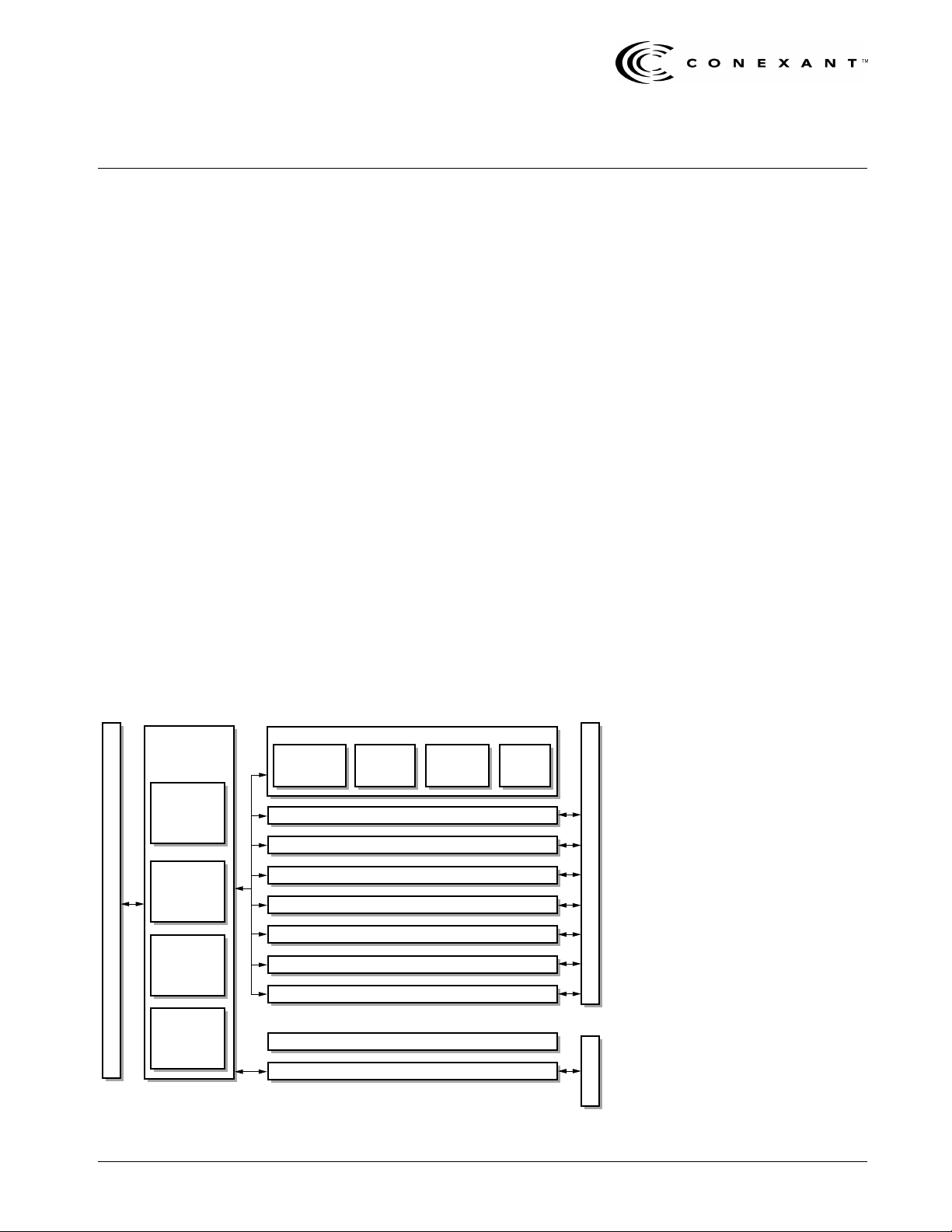
Functional Block Diagram
Channel Group 0 – Serial Interface
DMA
Controller
Interrupt
Controller
Channel Group 1 – Serial Interface
Channel Group 2 – Serial Interface
Channel Group 3 – Serial Interface
Channel Group 4 – Serial Interface
Channel Group 5 – Serial Interface
Channel Group 6 – Serial Interface
Channel Group 7 – Serial Interface
Boundary Scan and Test Access
Expanion Bus Interface
Bit-Level
Processor
Tx/Rx-BLP
Port
Interface
Tx/Rx
PCI Bus
Host
Interface
Device
Configuration
Registers
PCI
Interface
PCI
Configuration
Space
(Function 0)
PCI
Configuration
Space
(Function 1)
Tx/Rx-DMAC
Note: Number of serial interfaces is device-dependent.
Distinguishing Features
• 256-, 128-, 64-, or 32-channel HDLC
controller
• OSI Layer 2 protocol support
• General purpose HDLC (ISO 3309)
– X.25 (LAPB)
– Frame relay (LAPF/ANSI T1.618)
– ISDN D-channel (LAPD/Q.921)
– SS7 support
• 8, 4, 2, or 1 independent serial interfaces
which support
– T1/E1 data streams
– DC to 8.192 Mbps TDM busses
• Configurable logical channels
– Standard DS0 (56, 64 kbps)
– Hyperchannel (Nx64)
– Subchannel (Nx8)
• Per-channel protocol mode selection
– 16-bit FCS mode
– 32-bit FCS mode
– SS7 mode (16-bit FCS)
– Transparent mode (unformatted data)
• Per-channel DMA buffer management
– Linked list data structures
– Variable size transmit/receive FIFO
• Per-channel message length check
– Select no length checking
– Select from two 12-bit registers to
compare message length
– Maximum length 16,384 Bytes
• Direct PCI bus interface
– 32-bit, 66 or 33 MHz operation
– Bus master and slave operation
– PCI Version 2.1
• Local Expansion Bus interface (EBUS)
– 32-bit multiplexed address/data bus
– Burst access up to 64 Bytes
• Low power, 3.3/2.5 V CMOS operation
• JTAG boundary scan access port
• 208-pin PQFP/surface-mount package
•BGA
Serial Data Bus
Applications
• ISDN basic-rate or primary-rate interfaces
• ISDN D-channel controller
•Routers
• Cellular base station switch controller
• CSU/DSU
• Protocol converter
• Packet data switch
• Frame relay switches/Frame Relay Access
Devices (FRAD)
• DXI network interface
Local Bus
• Distributed packet-based communications
system
• Access multiplexer/concentrator
100660E Conexant
Page 2

Ordering Information
Model Number Version Package Temperature Range
CN8471AEPF 32-Channel 208-Pin Plastic Quad Flat Pack (PQFP) –40 °C to +85 °C
CN8472AEPF 64-Channel 208-Pin Plastic Quad Flat Pack (PQFP) –40 °C to +85 °C
CN8474AEPF 128-Channel 208-Pin Plastic Quad Flat Pack (PQFP) –40 °C to +85 °C
CN8478EPF 256-Channel 208-Pin Plastic Quad Flat Pack (PQFP) –40 °C to +85 °C
CN8471AEBG 32-Channel 208-Pin Plastic Ball Grid Array –40 °C to +85 °C
CN8472AEBG 64-Channel 208-Pin Plastic Ball Grid Array –40 °C to +85 °C
CN8474AEBG 128-Channel 208-Pin Plastic Ball Grid Array –40 °C to +85 °C
CN8478EBG 256-Channel 208-Pin Plastic Ball Grid Array –40 °C to +85 °C
© 2000, Conexant Systems,Inc.
All Rights Reserved.
Information in this document is provided in connection with Conexant Systems, Inc. (“Conexant”) products. These materials are
provided by Conexant as a service to its customers and may b e used for informational purposes only. Conexant assumes no
responsibility for errors or omissions in these materials. Conexant may make changes to specifications and product descriptions at
any time, without not ice. Conexant makes no commitment to update the information and sha ll have no responsibility whatsoever for
conflicts or incompatibilities arising from future changes to its specifications and product descriptions.
No license, express or implied, by estoppel or otherwise, to any intellectual property rights is granted by this document. Except as
provided in Conexant’s Terms and Conditions of Sale for such products, Conexant assumes no liability whatsoever.
THESE MATERIALSARE PROVIDED “AS IS” WITHOUT WARRANTY OF ANY KIND, EITHER EXPRESS OR IMPLIED,RELATING
TO SALE AND/OR USE OF CONEXANT P RODUCTS INCLUDING LIABILITY OR WARRANTIES RELATING TO FITNESS FOR A
PARTICULAR PURPOSE, CONSEQUENTIAL OR INCIDENTAL DAMAGES, MERCHANTABILITY, OR INFRINGEMENT OF A NY
PATENT, COPYRIGHT OR OTHER INTELLECTUAL PROPERTY RIGHT.CONEXANT FURTHER DOES NOT WARRANT THE
ACCURACY OR COMPLETENESS OF THE INFORMATION, TEXT,GRAPHICS OR OTHER ITEMS CONTAINED W ITHIN THESE
MATERIALS. CONEXANT SHALL NOT BE LIABLE FOR ANY SPECIAL, INDIRECT,INCIDENTAL, OR CONSEQUENTIAL
DAMAGES,INCLUDING WITHOUT LIMITATION, LOST REVENUES OR LOST PROFITS, WHICH MAY RESULTFROM THE USE
OF THESE MATERIALS.
Conexant products are not intended for us e in medical, lifesaving or life sustaining applications. Conexant customers us i ng or selling
Conexant products for use in such applications do so at their own risk and agree to fully indemnify Conexant for any damages
resulting from such improper use or sale.
The following are trademarks of Conexant Systems, Inc.: Conexant™, the Conexant C symbol, and “What’s Next in Communications
Technologies”™. Product names or services listed in this publication are for identification purposes only, and may be trademarks of
third parties. Third-party brands and names are the property of their respective owners.
For additional disclaimer information, please consult Conexant’s Legal Information posted at www.conexant.com,whichis
incorporated by reference.
Reader Response: Conexant strives to produce quality documentation and welcomes your feedback. Please send comments and
suggestions to tech.pubs@conexant.com. For technical questions, contact your local Conexant sales office or field applications
engineer.
100660E Conexant
Page 3

Table of Contents
List of Figures. . . . . . . . . . . . . . . . . . . . . . . . . . . . . . . . . . . . . . . . . . . . . . . . . . . . . . . . . . . . . . . . . . . ix
List of Tables. . . . . . . . . . . . . . . . . . . . . . . . . . . . . . . . . . . . . . . . . . . . . . . . . . . . . . . . . . . . . . . . . . . . xi
1.0 System Description. . . . . . . . . . . . . . . . . . . . . . . . . . . . . . . . . . . . . . . . . . . . . . . . . . . . . . . . . . . . . 1-1
1.1 Pin Descriptions . . . . . . . . . . . . . . . . . . . . . . . . . . . . . . . . . . . . . . . . . . . . . . . . . . . . . . . . . . . . 1-5
2.0 Host Interface . . . . . . . . . . . . . . . . . . . . . . . . . . . . . . . . . . . . . . . . . . . . . . . . . . . . . . . . . . . . . . . . . . 2-1
2.1 PCI Interface . . . . . . . . . . . . . . . . . . . . . . . . . . . . . . . . . . . . . . . . . . . . . . . . . . . . . . . . . . . . . . . 2-2
2.1.1 PCI Initialization . . . . . . . . . . . . . . . . . . . . . . . . . . . . . . . . . . . . . . . . . . . . . . . . . . . . . . . 2-2
2.1.2 PCI Bus Operations . . . . . . . . . . . . . . . . . . . . . . . . . . . . . . . . . . . . . . . . . . . . . . . . . . . . 2-3
2.1.3 PCI Configuration Space. . . . . . . . . . . . . . . . . . . . . . . . . . . . . . . . . . . . . . . . . . . . . . . . . 2-3
2.2 PCI Configuration Registers . . . . . . . . . . . . . . . . . . . . . . . . . . . . . . . . . . . . . . . . . . . . . . . . . . . 2-7
2.2.1 Function 0 Network Controller—PCI Master and Slave. . . . . . . . . . . . . . . . . . . . . . . . . . . 2-7
2.2.2 Function 1 Expansion Bus Bridge, PCI Slave . . . . . . . . . . . . . . . . . . . . . . . . . . . . . . . . . 2-13
2.2.3 PCI Reset. . . . . . . . . . . . . . . . . . . . . . . . . . . . . . . . . . . . . . . . . . . . . . . . . . . . . . . . . . . 2-17
2.2.4 Host Interface . . . . . . . . . . . . . . . . . . . . . . . . . . . . . . . . . . . . . . . . . . . . . . . . . . . . . . . 2-17
2.2.5 PCI Bus Parity . . . . . . . . . . . . . . . . . . . . . . . . . . . . . . . . . . . . . . . . . . . . . . . . . . . . . . . 2-18
2.2.6 PCI Throughput and Latency Considerations . . . . . . . . . . . . . . . . . . . . . . . . . . . . . . . . . 2-18
2.2.6.1 PCI Bus Latency . . . . . . . . . . . . . . . . . . . . . . . . . . . . . . . . . . . . . . . . . . . . . 2-19
2.2.6.2 Latency Computation—Single Dword Access. . . . . . . . . . . . . . . . . . . . . . . . 2-21
2.2.6.3 Latency Computation—Burst Access . . . . . . . . . . . . . . . . . . . . . . . . . . . . . . 2-22
3.0 Expansion Bus (EBUS) . . . . . . . . . . . . . . . . . . . . . . . . . . . . . . . . . . . . . . . . . . . . . . . . . . . . . . . . . . 3-1
3.1 Operation . . . . . . . . . . . . . . . . . . . . . . . . . . . . . . . . . . . . . . . . . . . . . . . . . . . . . . . . . . . . . . . . . 3-2
3.1.1 Initialization . . . . . . . . . . . . . . . . . . . . . . . . . . . . . . . . . . . . . . . . . . . . . . . . . . . . . . . . . . 3-2
3.1.2 Address and Data. . . . . . . . . . . . . . . . . . . . . . . . . . . . . . . . . . . . . . . . . . . . . . . . . . . . . . 3-2
3.1.3 Clock . . . . . . . . . . . . . . . . . . . . . . . . . . . . . . . . . . . . . . . . . . . . . . . . . . . . . . . . . . . . . . . 3-3
3.1.4 Interrupt . . . . . . . . . . . . . . . . . . . . . . . . . . . . . . . . . . . . . . . . . . . . . . . . . . . . . . . . . . . . 3-4
3.1.5 Address Duration . . . . . . . . . . . . . . . . . . . . . . . . . . . . . . . . . . . . . . . . . . . . . . . . . . . . . . 3-4
3.1.6 Data Duration. . . . . . . . . . . . . . . . . . . . . . . . . . . . . . . . . . . . . . . . . . . . . . . . . . . . . . . . . 3-4
3.1.7 Bus Access Interval . . . . . . . . . . . . . . . . . . . . . . . . . . . . . . . . . . . . . . . . . . . . . . . . . . . . 3-5
3.1.8 PCI to EBUS Interaction . . . . . . . . . . . . . . . . . . . . . . . . . . . . . . . . . . . . . . . . . . . . . . . . . 3-5
3.1.9 Microprocessor Interface . . . . . . . . . . . . . . . . . . . . . . . . . . . . . . . . . . . . . . . . . . . . . . . . 3-6
3.1.10 Arbitration . . . . . . . . . . . . . . . . . . . . . . . . . . . . . . . . . . . . . . . . . . . . . . . . . . . . . . . . . . . 3-7
3.1.11 Connection . . . . . . . . . . . . . . . . . . . . . . . . . . . . . . . . . . . . . . . . . . . . . . . . . . . . . . . . . . 3-8
100660E Conexant iii
Page 4

Table of Contents CN8478/CN8474A/CN8472A/CN8471A
Multichannel Synchronous Communications Controller (MUSYCC™)
4.0 Serial Interface. . . . . . . . . . . . . . . . . . . . . . . . . . . . . . . . . . . . . . . . . . . . . . . . . . . . . . . . . . . . . . . . .4-1
4.1 Serial Port Interface . . . . . . . . . . . . . . . . . . . . . . . . . . . . . . . . . . . . . . . . . . . . . . . . . . . . . . . . . 4-2
4.2 Bit Level Processor. . . . . . . . . . . . . . . . . . . . . . . . . . . . . . . . . . . . . . . . . . . . . . . . . . . . . . . . . . 4-2
4.3 DMA Controller . . . . . . . . . . . . . . . . . . . . . . . . . . . . . . . . . . . . . . . . . . . . . . . . . . . . . . . . . . . . . 4-2
4.4 Interrupt Controller . . . . . . . . . . . . . . . . . . . . . . . . . . . . . . . . . . . . . . . . . . . . . . . . . . . . . . . . . . 4-2
4.5 Channelized Port Mode . . . . . . . . . . . . . . . . . . . . . . . . . . . . . . . . . . . . . . . . . . . . . . . . . . . . . . . 4-3
4.5.1 Hyperchannels (Nx64) . . . . . . . . . . . . . . . . . . . . . . . . . . . . . . . . . . . . . . . . . . . . . . . . . . 4-3
4.5.2 Subchannels (Nx8). . . . . . . . . . . . . . . . . . . . . . . . . . . . . . . . . . . . . . . . . . . . . . . . . . . . . 4-3
4.5.3 Frame Synchronization Flywheel. . . . . . . . . . . . . . . . . . . . . . . . . . . . . . . . . . . . . . . . . . . 4-4
4.5.4 Change-of-Frame Alignment . . . . . . . . . . . . . . . . . . . . . . . . . . . . . . . . . . . . . . . . . . . . . . 4-8
4.5.5 Out-of-Frame . . . . . . . . . . . . . . . . . . . . . . . . . . . . . . . . . . . . . . . . . . . . . . . . . . . . . . . . . 4-8
4.6 Serial Port Mapping . . . . . . . . . . . . . . . . . . . . . . . . . . . . . . . . . . . . . . . . . . . . . . . . . . . . . . . . . 4-9
4.7 Tx and Rx FIFO Buffer Allocation and Management. . . . . . . . . . . . . . . . . . . . . . . . . . . . . . . . . 4-11
4.7.1 Example Channel BUFFLOC and BUFFLEN Specification. . . . . . . . . . . . . . . . . . . . . . . . . 4-13
4.7.2 Receiving Bit Stream . . . . . . . . . . . . . . . . . . . . . . . . . . . . . . . . . . . . . . . . . . . . . . . . . . 4-15
4.7.3 Transmitting Bit Stream . . . . . . . . . . . . . . . . . . . . . . . . . . . . . . . . . . . . . . . . . . . . . . . . 4-15
4.7.3.1 Transmit Data Bit Output Value Determination . . . . . . . . . . . . . . . . . . . . . . . 4-16
5.0 Memory Organization . . . . . . . . . . . . . . . . . . . . . . . . . . . . . . . . . . . . . . . . . . . . . . . . . . . . . . . . . . . 5-1
5.1 Memory Architecture. . . . . . . . . . . . . . . . . . . . . . . . . . . . . . . . . . . . . . . . . . . . . . . . . . . . . . . . . 5-1
5.1.1 Register Map Access and Shared Memory Access. . . . . . . . . . . . . . . . . . . . . . . . . . . . . . 5-3
5.1.2 Memory Access Illustration . . . . . . . . . . . . . . . . . . . . . . . . . . . . . . . . . . . . . . . . . . . . . . 5-6
5.2 Descriptors . . . . . . . . . . . . . . . . . . . . . . . . . . . . . . . . . . . . . . . . . . . . . . . . . . . . . . . . . . . . . . . . 5-9
5.2.1 Host Interface Level Descriptors . . . . . . . . . . . . . . . . . . . . . . . . . . . . . . . . . . . . . . . . . . 5-10
5.2.1.1 Global Configuration Descriptor. . . . . . . . . . . . . . . . . . . . . . . . . . . . . . . . . . 5-10
5.2.1.2 Dual Address Cycle Base Pointer . . . . . . . . . . . . . . . . . . . . . . . . . . . . . . . . . 5-12
5.2.2 Channel Group Level Descriptors . . . . . . . . . . . . . . . . . . . . . . . . . . . . . . . . . . . . . . . . . 5-12
5.2.2.1 Group Base Pointer . . . . . . . . . . . . . . . . . . . . . . . . . . . . . . . . . . . . . . . . . . . 5-12
5.2.2.2 Service Request . . . . . . . . . . . . . . . . . . . . . . . . . . . . . . . . . . . . . . . . . . . . . 5-13
5.2.2.3 Group Configuration Descriptor. . . . . . . . . . . . . . . . . . . . . . . . . . . . . . . . . . 5-16
5.2.2.4 Memory Protection Descriptor. . . . . . . . . . . . . . . . . . . . . . . . . . . . . . . . . . . 5-18
5.2.2.5 Port Configuration Descriptor . . . . . . . . . . . . . . . . . . . . . . . . . . . . . . . . . . . 5-18
5.2.2.6 Message Length Descriptor. . . . . . . . . . . . . . . . . . . . . . . . . . . . . . . . . . . . . 5-20
5.2.2.7 Time Slot Map . . . . . . . . . . . . . . . . . . . . . . . . . . . . . . . . . . . . . . . . . . . . . . 5-20
5.2.2.8 Subchannel Map . . . . . . . . . . . . . . . . . . . . . . . . . . . . . . . . . . . . . . . . . . . . . 5-24
5.2.3 Channel Level Descriptors . . . . . . . . . . . . . . . . . . . . . . . . . . . . . . . . . . . . . . . . . . . . . . 5-26
5.2.3.1 Channel Configuration Descriptor . . . . . . . . . . . . . . . . . . . . . . . . . . . . . . . . 5-26
5.2.4 Message Level Descriptor. . . . . . . . . . . . . . . . . . . . . . . . . . . . . . . . . . . . . . . . . . . . . . . 5-29
5.2.4.1 Using Message Descriptors. . . . . . . . . . . . . . . . . . . . . . . . . . . . . . . . . . . . . 5-30
5.2.4.2 Note for Interrupt Driven Drivers . . . . . . . . . . . . . . . . . . . . . . . . . . . . . . . . . 5-31
5.2.4.3 Head Pointer . . . . . . . . . . . . . . . . . . . . . . . . . . . . . . . . . . . . . . . . . . . . . . . . 5-31
5.2.4.4 Message Pointer . . . . . . . . . . . . . . . . . . . . . . . . . . . . . . . . . . . . . . . . . . . . . 5-31
5.2.4.5 Message Descriptor . . . . . . . . . . . . . . . . . . . . . . . . . . . . . . . . . . . . . . . . . . 5-32
5.2.4.6 Buffer Descriptor. . . . . . . . . . . . . . . . . . . . . . . . . . . . . . . . . . . . . . . . . . . . . 5-32
iv Conexant 100660E
Page 5

CN8478/CN8474A/CN8472A/CN8471A Table of Contents
Multichannel Synchronous Communications Controller (MUSYCC™)
5.2.4.7 Buffer Status Descriptor . . . . . . . . . . . . . . . . . . . . . . . . . . . . . . . . . . . . . . . 5-34
5.2.4.8 Next Message Pointer . . . . . . . . . . . . . . . . . . . . . . . . . . . . . . . . . . . . . . . . . 5-37
5.2.4.9 Data Buffer Pointer . . . . . . . . . . . . . . . . . . . . . . . . . . . . . . . . . . . . . . . . . . . 5-37
5.2.4.10 Message Descriptor Handling . . . . . . . . . . . . . . . . . . . . . . . . . . . . . . . . . . . 5-37
5.2.5 Interrupt Level Descriptors . . . . . . . . . . . . . . . . . . . . . . . . . . . . . . . . . . . . . . . . . . . . . . 5-38
5.2.5.1 Interrupt Queue Descriptor . . . . . . . . . . . . . . . . . . . . . . . . . . . . . . . . . . . . . 5-38
5.2.5.2 Interrupt Descriptor . . . . . . . . . . . . . . . . . . . . . . . . . . . . . . . . . . . . . . . . . . 5-39
5.2.5.3 Interrupt Status Descriptor . . . . . . . . . . . . . . . . . . . . . . . . . . . . . . . . . . . . . 5-44
5.2.6 Interrupt Handling . . . . . . . . . . . . . . . . . . . . . . . . . . . . . . . . . . . . . . . . . . . . . . . . . . . . 5-45
5.2.6.1 Initialization . . . . . . . . . . . . . . . . . . . . . . . . . . . . . . . . . . . . . . . . . . . . . . . . 5-45
5.2.6.2 Interrupt Descriptor Generation . . . . . . . . . . . . . . . . . . . . . . . . . . . . . . . . . . 5-45
5.2.6.3 INTA* Signal Line . . . . . . . . . . . . . . . . . . . . . . . . . . . . . . . . . . . . . . . . . . . . 5-46
5.2.6.4 INTB* Signal Line . . . . . . . . . . . . . . . . . . . . . . . . . . . . . . . . . . . . . . . . . . . . 5-46
6.0 Basic Operation . . . . . . . . . . . . . . . . . . . . . . . . . . . . . . . . . . . . . . . . . . . . . . . . . . . . . . . . . . . . . . . .6-1
6.1 Reset . . . . . . . . . . . . . . . . . . . . . . . . . . . . . . . . . . . . . . . . . . . . . . . . . . . . . . . . . . . . . . . . . . . . 6-1
6.1.1 Hard PCI Reset . . . . . . . . . . . . . . . . . . . . . . . . . . . . . . . . . . . . . . . . . . . . . . . . . . . . . . . 6-1
6.1.2 Soft Chip Reset . . . . . . . . . . . . . . . . . . . . . . . . . . . . . . . . . . . . . . . . . . . . . . . . . . . . . . . 6-2
6.1.3 Soft Group Reset . . . . . . . . . . . . . . . . . . . . . . . . . . . . . . . . . . . . . . . . . . . . . . . . . . . . . . 6-3
6.1.4 Initialization Sequence Example . . . . . . . . . . . . . . . . . . . . . . . . . . . . . . . . . . . . . . . . . . . 6-3
6.2 Configuration . . . . . . . . . . . . . . . . . . . . . . . . . . . . . . . . . . . . . . . . . . . . . . . . . . . . . . . . . . . . . . 6-4
6.2.1 PCI Configuration. . . . . . . . . . . . . . . . . . . . . . . . . . . . . . . . . . . . . . . . . . . . . . . . . . . . . . 6-4
6.2.2 Global Configuration. . . . . . . . . . . . . . . . . . . . . . . . . . . . . . . . . . . . . . . . . . . . . . . . . . . . 6-5
6.2.3 Interrupt Queue Configuration. . . . . . . . . . . . . . . . . . . . . . . . . . . . . . . . . . . . . . . . . . . . . 6-5
6.2.4 Channel Group(s) Configuration . . . . . . . . . . . . . . . . . . . . . . . . . . . . . . . . . . . . . . . . . . . 6-5
6.2.5 Service Request Mechanism. . . . . . . . . . . . . . . . . . . . . . . . . . . . . . . . . . . . . . . . . . . . . . 6-5
6.2.6 MUSYCC Internal Memory . . . . . . . . . . . . . . . . . . . . . . . . . . . . . . . . . . . . . . . . . . . . . . . 6-6
6.2.6.1 Memory Operations—Inactive Channels . . . . . . . . . . . . . . . . . . . . . . . . . . . . 6-6
6.2.6.2 Memory Operations—Active Channels. . . . . . . . . . . . . . . . . . . . . . . . . . . . . . 6-6
6.3 Channel Operation . . . . . . . . . . . . . . . . . . . . . . . . . . . . . . . . . . . . . . . . . . . . . . . . . . . . . . . . . . 6-8
6.3.1 Group Structure. . . . . . . . . . . . . . . . . . . . . . . . . . . . . . . . . . . . . . . . . . . . . . . . . . . . . . . 6-8
6.3.2 Group Base Pointer . . . . . . . . . . . . . . . . . . . . . . . . . . . . . . . . . . . . . . . . . . . . . . . . . . . 6-10
6.3.3 Global Configuration Descriptor . . . . . . . . . . . . . . . . . . . . . . . . . . . . . . . . . . . . . . . . . . 6-11
6.3.4 Interrupt Queue Descriptor . . . . . . . . . . . . . . . . . . . . . . . . . . . . . . . . . . . . . . . . . . . . . . 6-12
6.3.5 Group Configuration Descriptor . . . . . . . . . . . . . . . . . . . . . . . . . . . . . . . . . . . . . . . . . . 6-13
6.3.6 Memory Protection Descriptor . . . . . . . . . . . . . . . . . . . . . . . . . . . . . . . . . . . . . . . . . . . 6-14
6.3.7 Port Configuration Descriptor . . . . . . . . . . . . . . . . . . . . . . . . . . . . . . . . . . . . . . . . . . . . 6-14
6.3.8 Message Length Descriptor . . . . . . . . . . . . . . . . . . . . . . . . . . . . . . . . . . . . . . . . . . . . . 6-15
6.3.9 Transmit Time Slot Map—Channel 0 . . . . . . . . . . . . . . . . . . . . . . . . . . . . . . . . . . . . . . . 6-15
6.3.10 Transmit Subchannel Map . . . . . . . . . . . . . . . . . . . . . . . . . . . . . . . . . . . . . . . . . . . . . . 6-16
6.3.11 Transmit Channel Configuration Descriptor . . . . . . . . . . . . . . . . . . . . . . . . . . . . . . . . . . 6-17
6.3.12 Receive Time Slot Map . . . . . . . . . . . . . . . . . . . . . . . . . . . . . . . . . . . . . . . . . . . . . . . . . 6-19
6.3.13 Receive Subchannel Map . . . . . . . . . . . . . . . . . . . . . . . . . . . . . . . . . . . . . . . . . . . . . . . 6-19
6.3.14 Receive Channel Configuration Descriptor. . . . . . . . . . . . . . . . . . . . . . . . . . . . . . . . . . . 6-19
6.3.15 Message Lists . . . . . . . . . . . . . . . . . . . . . . . . . . . . . . . . . . . . . . . . . . . . . . . . . . . . . . . 6-19
100660E Conexant v
Preliminary Information
Page 6

Table of Contents CN8478/CN8474A/CN8472A/CN8471A
Multichannel Synchronous Communications Controller (MUSYCC™)
6.3.16 Channel Activation . . . . . . . . . . . . . . . . . . . . . . . . . . . . . . . . . . . . . . . . . . . . . . . . . . . . 6-21
6.3.16.1 Transmit Channel Activation . . . . . . . . . . . . . . . . . . . . . . . . . . . . . . . . . . . . 6-21
6.3.16.2 Receive Channel Activation . . . . . . . . . . . . . . . . . . . . . . . . . . . . . . . . . . . . . 6-22
6.3.17 Channel Deactivation . . . . . . . . . . . . . . . . . . . . . . . . . . . . . . . . . . . . . . . . . . . . . . . . . . 6-23
6.3.17.1 Transmit Channel Deactivation. . . . . . . . . . . . . . . . . . . . . . . . . . . . . . . . . . . 6-23
6.3.17.2 Receive Channel Deactivation . . . . . . . . . . . . . . . . . . . . . . . . . . . . . . . . . . . 6-23
6.3.18 Channel Jump . . . . . . . . . . . . . . . . . . . . . . . . . . . . . . . . . . . . . . . . . . . . . . . . . . . . . . . 6-24
6.3.19 Frame Alignment . . . . . . . . . . . . . . . . . . . . . . . . . . . . . . . . . . . . . . . . . . . . . . . . . . . . . 6-24
6.3.20 Descriptor Polling . . . . . . . . . . . . . . . . . . . . . . . . . . . . . . . . . . . . . . . . . . . . . . . . . . . . 6-25
6.3.21 Repeat Message Transmission . . . . . . . . . . . . . . . . . . . . . . . . . . . . . . . . . . . . . . . . . . . 6-26
6.4 Protocol Support . . . . . . . . . . . . . . . . . . . . . . . . . . . . . . . . . . . . . . . . . . . . . . . . . . . . . . . . . . . 6-28
6.4.1 Frame Check Sequence . . . . . . . . . . . . . . . . . . . . . . . . . . . . . . . . . . . . . . . . . . . . . . . . 6-28
6.4.2 Opening/Closing Flags . . . . . . . . . . . . . . . . . . . . . . . . . . . . . . . . . . . . . . . . . . . . . . . . . 6-28
6.4.3 Abort Codes. . . . . . . . . . . . . . . . . . . . . . . . . . . . . . . . . . . . . . . . . . . . . . . . . . . . . . . . . 6-28
6.4.4 Zero-Bit Insertion/Deletion . . . . . . . . . . . . . . . . . . . . . . . . . . . . . . . . . . . . . . . . . . . . . . 6-29
6.4.5 Message Configuration Bits . . . . . . . . . . . . . . . . . . . . . . . . . . . . . . . . . . . . . . . . . . . . . 6-29
6.4.5.1 Idle Code . . . . . . . . . . . . . . . . . . . . . . . . . . . . . . . . . . . . . . . . . . . . . . . . . . 6-29
6.4.5.2 Inter-message Pad Fill. . . . . . . . . . . . . . . . . . . . . . . . . . . . . . . . . . . . . . . . . 6-29
6.4.5.3 Repeat Message Transmission. . . . . . . . . . . . . . . . . . . . . . . . . . . . . . . . . . . 6-29
6.4.6 Message Configuration Bits Copy Enable/Disable. . . . . . . . . . . . . . . . . . . . . . . . . . . . . . 6-29
6.4.7 Bit-Level Operation. . . . . . . . . . . . . . . . . . . . . . . . . . . . . . . . . . . . . . . . . . . . . . . . . . . . 6-31
6.4.7.1 Transmit . . . . . . . . . . . . . . . . . . . . . . . . . . . . . . . . . . . . . . . . . . . . . . . . . . . 6-32
6.4.7.2 Receive. . . . . . . . . . . . . . . . . . . . . . . . . . . . . . . . . . . . . . . . . . . . . . . . . . . . 6-32
6.4.8 HDLC Mode . . . . . . . . . . . . . . . . . . . . . . . . . . . . . . . . . . . . . . . . . . . . . . . . . . . . . . . . . 6-33
6.4.8.1 Transmit Events . . . . . . . . . . . . . . . . . . . . . . . . . . . . . . . . . . . . . . . . . . . . . 6-33
6.4.8.2 Receive Events . . . . . . . . . . . . . . . . . . . . . . . . . . . . . . . . . . . . . . . . . . . . . . 6-34
6.4.8.3 Transmit Errors . . . . . . . . . . . . . . . . . . . . . . . . . . . . . . . . . . . . . . . . . . . . . . 6-36
6.4.8.4 Receive Errors . . . . . . . . . . . . . . . . . . . . . . . . . . . . . . . . . . . . . . . . . . . . . . 6-37
6.4.9 Transparent Mode . . . . . . . . . . . . . . . . . . . . . . . . . . . . . . . . . . . . . . . . . . . . . . . . . . . . 6-43
6.4.9.1 Transmit Events . . . . . . . . . . . . . . . . . . . . . . . . . . . . . . . . . . . . . . . . . . . . . 6-44
6.4.9.2 Receive Events . . . . . . . . . . . . . . . . . . . . . . . . . . . . . . . . . . . . . . . . . . . . . . 6-44
6.4.9.3 Transmit Errors . . . . . . . . . . . . . . . . . . . . . . . . . . . . . . . . . . . . . . . . . . . . . . 6-45
6.4.9.4 Receive Errors . . . . . . . . . . . . . . . . . . . . . . . . . . . . . . . . . . . . . . . . . . . . . . 6-46
6.4.10 Intersystem Link Protocol (ISLP) . . . . . . . . . . . . . . . . . . . . . . . . . . . . . . . . . . . . . . . . . 6-48
6.5 Signaling System 7. . . . . . . . . . . . . . . . . . . . . . . . . . . . . . . . . . . . . . . . . . . . . . . . . . . . . . . . . 6-49
6.5.1 SS7 Repeat Message Transmission. . . . . . . . . . . . . . . . . . . . . . . . . . . . . . . . . . . . . . . . 6-49
6.5.2 Message Filtering . . . . . . . . . . . . . . . . . . . . . . . . . . . . . . . . . . . . . . . . . . . . . . . . . . . . . 6-49
6.5.3 Signal Unit Error Rate Monitoring . . . . . . . . . . . . . . . . . . . . . . . . . . . . . . . . . . . . . . . . . 6-50
6.5.4 SUERM Counter Incrementing . . . . . . . . . . . . . . . . . . . . . . . . . . . . . . . . . . . . . . . . . . . 6-50
6.5.5 SUERM Octet Counting . . . . . . . . . . . . . . . . . . . . . . . . . . . . . . . . . . . . . . . . . . . . . . . . 6-50
6.5.6 SUERM Counter Decrementing. . . . . . . . . . . . . . . . . . . . . . . . . . . . . . . . . . . . . . . . . . . 6-50
6.6 Self-Servicing Buffers . . . . . . . . . . . . . . . . . . . . . . . . . . . . . . . . . . . . . . . . . . . . . . . . . . . . . . . 6-51
vi Conexant 100660E
Page 7

CN8478/CN8474A/CN8472A/CN8471A Table of Contents
Multichannel Synchronous Communications Controller (MUSYCC™)
7.0 Electrical and Mechanical Specifications . . . . . . . . . . . . . . . . . . . . . . . . . . . . . . . . . . . . . . . . . 7-1
7.1 Electrical and Environmental Specifications . . . . . . . . . . . . . . . . . . . . . . . . . . . . . . . . . . . . . . . 7-1
7.1.1 Absolute Maximum Ratings . . . . . . . . . . . . . . . . . . . . . . . . . . . . . . . . . . . . . . . . . . . . . . 7-1
7.1.2 Recommended Operating Conditions . . . . . . . . . . . . . . . . . . . . . . . . . . . . . . . . . . . . . . . 7-2
7.1.3 Electrical Characteristics. . . . . . . . . . . . . . . . . . . . . . . . . . . . . . . . . . . . . . . . . . . . . . . . . 7-2
7.2 Timing and Switching Specifications. . . . . . . . . . . . . . . . . . . . . . . . . . . . . . . . . . . . . . . . . . . . . 7-3
7.2.1 Overview . . . . . . . . . . . . . . . . . . . . . . . . . . . . . . . . . . . . . . . . . . . . . . . . . . . . . . . . . . . . 7-3
7.2.2 Host Interface (PCI) Timing and Switching Characteristic. . . . . . . . . . . . . . . . . . . . . . . . . 7-3
7.2.3 Expansion Bus (EBUS) Timing and Switching Characteristic . . . . . . . . . . . . . . . . . . . . . 7-11
7.2.4 EBUS Arbitration Timing. . . . . . . . . . . . . . . . . . . . . . . . . . . . . . . . . . . . . . . . . . . . . . . . 7-14
7.2.5 Serial Interface Timing and Switching Characteristics . . . . . . . . . . . . . . . . . . . . . . . . . . 7-16
7.2.6 Package Thermal Specification . . . . . . . . . . . . . . . . . . . . . . . . . . . . . . . . . . . . . . . . . . . 7-18
7.2.7 Mechanical Specifications. . . . . . . . . . . . . . . . . . . . . . . . . . . . . . . . . . . . . . . . . . . . . . . 7-19
8.0 Terms, Definitions, and Conventions . . . . . . . . . . . . . . . . . . . . . . . . . . . . . . . . . . . . . . . . . . . . . 8-1
8.1 Applicable Specifications . . . . . . . . . . . . . . . . . . . . . . . . . . . . . . . . . . . . . . . . . . . . . . . . . . . . . 8-1
8.2 Numeric Notation . . . . . . . . . . . . . . . . . . . . . . . . . . . . . . . . . . . . . . . . . . . . . . . . . . . . . . . . . . . 8-2
8.3 Bit Stream Transmission Convention. . . . . . . . . . . . . . . . . . . . . . . . . . . . . . . . . . . . . . . . . . . . . 8-3
8.4 Bit Stream Storage Convention . . . . . . . . . . . . . . . . . . . . . . . . . . . . . . . . . . . . . . . . . . . . . . . . . 8-4
8.5 Acronyms . . . . . . . . . . . . . . . . . . . . . . . . . . . . . . . . . . . . . . . . . . . . . . . . . . . . . . . . . . . . . . . . . 8-5
8.6 Definitions . . . . . . . . . . . . . . . . . . . . . . . . . . . . . . . . . . . . . . . . . . . . . . . . . . . . . . . . . . . . . . . . 8-7
8.7 Revision History . . . . . . . . . . . . . . . . . . . . . . . . . . . . . . . . . . . . . . . . . . . . . . . . . . . . . . . . . . . . 8-9
Appendix A JTAG Interface . . . . . . . . . . . . . . . . . . . . . . . . . . . . . . . . . . . . . . . . . . . . . . . . . . . . . . . . . . . . A-1
A.1 Instruction Register . . . . . . . . . . . . . . . . . . . . . . . . . . . . . . . . . . . . . . . . . . . . . . . . . . . . . . . . . A-1
A.2 BYPASS Register . . . . . . . . . . . . . . . . . . . . . . . . . . . . . . . . . . . . . . . . . . . . . . . . . . . . . . . . . . . A-2
100660E Conexant vii
Preliminary Information
Page 8

Table of Contents CN8478/CN8474A/CN8472A/CN8471A
Multichannel Synchronous Communications Controller (MUSYCC™)
viii Conexant 100660E
Page 9

CN8478/CN8474A/CN8472A/CN8471A List of Figures
Multichannel Synchronous Communications Controller (MUSYCC™)
List of Figures
Figure 1-1. System Block Diagram . . . . . . . . . . . . . . . . . . . . . . . . . . . . . . . . . . . . . . . . . . . . . . . . . . . . 1-1
Figure 1-2. Detailed System Block Diagram . . . . . . . . . . . . . . . . . . . . . . . . . . . . . . . . . . . . . . . . . . . . . 1-3
Figure 1-3. MUSYCC Application Example—Frame Relay Switch . . . . . . . . . . . . . . . . . . . . . . . . . . . . . 1-4
Figure 1-4. CN8478 MQFP Pinout Configuration . . . . . . . . . . . . . . . . . . . . . . . . . . . . . . . . . . . . . . . . . . 1-5
Figure 1-5. CN8474A MPQF Pinout Configuration. . . . . . . . . . . . . . . . . . . . . . . . . . . . . . . . . . . . . . . . . 1-8
Figure 1-6. CN8472A MQFP Pinout Configuration. . . . . . . . . . . . . . . . . . . . . . . . . . . . . . . . . . . . . . . . . 1-9
Figure 1-7. CN8471A MQFP Pinout Configuration. . . . . . . . . . . . . . . . . . . . . . . . . . . . . . . . . . . . . . . . 1-10
Figure 1-8. CN8478 PBGA Pinout Configuration (Top View) . . . . . . . . . . . . . . . . . . . . . . . . . . . . . . . . 1-11
Figure 1-9. CN8474A PBGA Pinout Configuration (Top View) . . . . . . . . . . . . . . . . . . . . . . . . . . . . . . . 1-14
Figure 1-10. CN8472A PBGA Pinout Configuration (Top View) . . . . . . . . . . . . . . . . . . . . . . . . . . . . . . . 1-15
Figure 1-11. CN8471A PBGA Pinout Configuration (Top View) . . . . . . . . . . . . . . . . . . . . . . . . . . . . . . . 1-16
Figure 1-12. CN8478 Logic Diagram . . . . . . . . . . . . . . . . . . . . . . . . . . . . . . . . . . . . . . . . . . . . . . . . . . . 1-17
Figure 2-1. Host Interface Functional Block Diagram. . . . . . . . . . . . . . . . . . . . . . . . . . . . . . . . . . . . . . . 2-1
Figure 2-2. Address Lines During Configuration Cycle . . . . . . . . . . . . . . . . . . . . . . . . . . . . . . . . . . . . . 2-4
Figure 3-1. EBUS Functional Block Diagram with Local MPU . . . . . . . . . . . . . . . . . . . . . . . . . . . . . . . . 3-1
Figure 3-2. EBUS Functional Block Diagram without Local MPU. . . . . . . . . . . . . . . . . . . . . . . . . . . . . . 3-1
Figure 3-3. EBUS Address/Data Line Structure . . . . . . . . . . . . . . . . . . . . . . . . . . . . . . . . . . . . . . . . . . .3-3
Figure 3-4. EBUS Connection, Non-multiplexed Address/Data, 8 Framers, No MPU. . . . . . . . . . . . . . . 3-8
Figure 3-5. EBUS Connection, Non-multiplexed Address/Data, 61 Framers, No MPU. . . . . . . . . . . . . . 3-9
Figure 3-6. EBUS Connection, Multiplexed Address/Data, 8 Framers, No MPU. . . . . . . . . . . . . . . . . . 3-10
Figure 4-1. Serial Interface Functional Block Diagram, Channel Group 0. . . . . . . . . . . . . . . . . . . . . . . . 4-1
Figure 4-2. Transmit and Receive T1 Mode . . . . . . . . . . . . . . . . . . . . . . . . . . . . . . . . . . . . . . . . . . . . . . 4-5
Figure 4-3. Transmit and Receive E1 (also 2xE1, 4xE1) Mode. . . . . . . . . . . . . . . . . . . . . . . . . . . . . . . . 4-6
Figure 4-4. Transmit and Receive Nx64 Mode . . . . . . . . . . . . . . . . . . . . . . . . . . . . . . . . . . . . . . . . . . . .4-7
Figure 4-5. Serial Port Mapping Options . . . . . . . . . . . . . . . . . . . . . . . . . . . . . . . . . . . . . . . . . . . . . . . . 4-9
Figure 4-6. Receive Data Flow . . . . . . . . . . . . . . . . . . . . . . . . . . . . . . . . . . . . . . . . . . . . . . . . . . . . . . . 4-11
Figure 4-7. Transmit Data Flow . . . . . . . . . . . . . . . . . . . . . . . . . . . . . . . . . . . . . . . . . . . . . . . . . . . . . . 4-12
Figure 4-8. Transmit Data Bit Output Value Determination . . . . . . . . . . . . . . . . . . . . . . . . . . . . . . . . . 4-16
Figure 5-1. Shared Memory Model Per Channel Group . . . . . . . . . . . . . . . . . . . . . . . . . . . . . . . . . . . . . 5-2
Figure 5-2. Interrupt Notification To Host . . . . . . . . . . . . . . . . . . . . . . . . . . . . . . . . . . . . . . . . . . . . . . 5-47
Figure 7-1. PCI Clock (PCLK) Waveform . . . . . . . . . . . . . . . . . . . . . . . . . . . . . . . . . . . . . . . . . . . . . . . . 7-5
Figure 7-2. PCI Reset Timing. . . . . . . . . . . . . . . . . . . . . . . . . . . . . . . . . . . . . . . . . . . . . . . . . . . . . . . . . 7-6
Figure 7-3. PCI Output Timing Waveform . . . . . . . . . . . . . . . . . . . . . . . . . . . . . . . . . . . . . . . . . . . . . . . 7-8
Figure 7-4. PCI Input Timing Waveform . . . . . . . . . . . . . . . . . . . . . . . . . . . . . . . . . . . . . . . . . . . . . . . . 7-9
Figure 7-5. PCI Read Multiple Operation . . . . . . . . . . . . . . . . . . . . . . . . . . . . . . . . . . . . . . . . . . . . . . . . 7-9
Figure 7-6. PCI Write Multiple Operation. . . . . . . . . . . . . . . . . . . . . . . . . . . . . . . . . . . . . . . . . . . . . . . 7-10
Figure 7-7. PCI Write Single Operation . . . . . . . . . . . . . . . . . . . . . . . . . . . . . . . . . . . . . . . . . . . . . . . . 7-10
Figure 7-8. ECLK to PCLK Relationship (M66EN = 0) . . . . . . . . . . . . . . . . . . . . . . . . . . . . . . . . . . . . . 7-11
Figure 7-9. ECLK to PCKL Relationship (M66EN = 1) . . . . . . . . . . . . . . . . . . . . . . . . . . . . . . . . . . . . . 7-11
100660E Conexant ix
Page 10

List of Figures CN8478/CN8474A/CN8472A/CN8471A
Multichannel Synchronous Communications Controller (MUSYCC™)
Figure 7-10. EBUS Reset Timing . . . . . . . . . . . . . . . . . . . . . . . . . . . . . . . . . . . . . . . . . . . . . . . . . . . . . . 7-12
Figure 7-11. EBUS Output Timing Waveform . . . . . . . . . . . . . . . . . . . . . . . . . . . . . . . . . . . . . . . . . . . . 7-13
Figure 7-12. EBUS Input Timing Waveform. . . . . . . . . . . . . . . . . . . . . . . . . . . . . . . . . . . . . . . . . . . . . .7-13
Figure 7-13. EBUS Write/Read Transactions, Intel-Style . . . . . . . . . . . . . . . . . . . . . . . . . . . . . . . . . . . . 7-14
Figure 7-14. EBUS Write/Read Transactions, Motorola-Style . . . . . . . . . . . . . . . . . . . . . . . . . . . . . . . . 7-15
Figure 7-15. Serial Interface Clock (RCLK,TCLK) Waveform . . . . . . . . . . . . . . . . . . . . . . . . . . . . . . . . . 7-16
Figure 7-16. Serial Interface Clock (RCLK,TCLK) Waveform . . . . . . . . . . . . . . . . . . . . . . . . . . . . . . . . . 7-17
Figure 7-17. Serial Interface Data Input Waveform . . . . . . . . . . . . . . . . . . . . . . . . . . . . . . . . . . . . . . . .7-17
Figure 7-18. Serial Interface Data Delay Output Waveform . . . . . . . . . . . . . . . . . . . . . . . . . . . . . . . . . . 7-18
Figure 7-19. 208-Pin Metric Quad Flatpack (MQFP) . . . . . . . . . . . . . . . . . . . . . . . . . . . . . . . . . . . . . . . 7-19
Figure 7-20. 208-Pin Plastic Ball Grid Array (PBGA) . . . . . . . . . . . . . . . . . . . . . . . . . . . . . . . . . . . . . . . 7-20
Figure A-1. JTAG Timing Diagram . . . . . . . . . . . . . . . . . . . . . . . . . . . . . . . . . . . . . . . . . . . . . . . . . . . . . A-3
x Conexant 100660E
Page 11

CN8478/CN8474A/CN8472A/CN8471A List of Tables
Multichannel Synchronous Communications Controller (MUSYCC™)
List of Tables
Table 1-1. CN8478 MQFP Pin List . . . . . . . . . . . . . . . . . . . . . . . . . . . . . . . . . . . . . . . . . . . . . . . . . . . . . 1-6
Table 1-2. CN8478 PBGA Pin List . . . . . . . . . . . . . . . . . . . . . . . . . . . . . . . . . . . . . . . . . . . . . . . . . . . . 1-12
Table 1-3. I/O Pin Types. . . . . . . . . . . . . . . . . . . . . . . . . . . . . . . . . . . . . . . . . . . . . . . . . . . . . . . . . . . . 1-18
Table 1-4. CN8478 Hardware Signal Definitions . . . . . . . . . . . . . . . . . . . . . . . . . . . . . . . . . . . . . . . . . 1-19
Table 2-1. Function 0 Configuration Space . . . . . . . . . . . . . . . . . . . . . . . . . . . . . . . . . . . . . . . . . . . . . . 2-5
Table 2-2. Function 1 Configuration Space . . . . . . . . . . . . . . . . . . . . . . . . . . . . . . . . . . . . . . . . . . . . . . 2-5
Table 2-3. Register 0, Address 00h . . . . . . . . . . . . . . . . . . . . . . . . . . . . . . . . . . . . . . . . . . . . . . . . . . . . 2-7
Table 2-4. Register 1, Address 04h . . . . . . . . . . . . . . . . . . . . . . . . . . . . . . . . . . . . . . . . . . . . . . . . . . . . 2-8
Table 2-5. Register 2, Address 08h . . . . . . . . . . . . . . . . . . . . . . . . . . . . . . . . . . . . . . . . . . . . . . . . . . . 2-10
Table 2-6. Register 3, Address 0Ch . . . . . . . . . . . . . . . . . . . . . . . . . . . . . . . . . . . . . . . . . . . . . . . . . . . 2-11
Table 2-7. Register 4, Address 10h . . . . . . . . . . . . . . . . . . . . . . . . . . . . . . . . . . . . . . . . . . . . . . . . . . . 2-12
Table 2-8. Registers 5–14, Addresses 14h–38h . . . . . . . . . . . . . . . . . . . . . . . . . . . . . . . . . . . . . . . . . 2-12
Table 2-9. Register 15, Address 3Ch . . . . . . . . . . . . . . . . . . . . . . . . . . . . . . . . . . . . . . . . . . . . . . . . . . 2-13
Table 2-10. Register 0, Address 00h . . . . . . . . . . . . . . . . . . . . . . . . . . . . . . . . . . . . . . . . . . . . . . . . . . . 2-14
Table 2-11. Register 1, Address 04h . . . . . . . . . . . . . . . . . . . . . . . . . . . . . . . . . . . . . . . . . . . . . . . . . . . 2-14
Table 2-12. Register 2, Address 08h . . . . . . . . . . . . . . . . . . . . . . . . . . . . . . . . . . . . . . . . . . . . . . . . . . . 2-15
Table 2-13. Register 3, Address 0Ch . . . . . . . . . . . . . . . . . . . . . . . . . . . . . . . . . . . . . . . . . . . . . . . . . . . 2-16
Table 2-14. Register 4, Address 10h . . . . . . . . . . . . . . . . . . . . . . . . . . . . . . . . . . . . . . . . . . . . . . . . . . . 2-16
Table 2-15. Registers 5 through 14–Addresses 14h through 38h . . . . . . . . . . . . . . . . . . . . . . . . . . . . . 2-16
Table 2-16. Register 15, Address 3Ch . . . . . . . . . . . . . . . . . . . . . . . . . . . . . . . . . . . . . . . . . . . . . . . . . . 2-17
Table 2-17. PCI Latency Example. . . . . . . . . . . . . . . . . . . . . . . . . . . . . . . . . . . . . . . . . . . . . . . . . . . . . . 2-20
Table 3-1. Intel Protocol Signals . . . . . . . . . . . . . . . . . . . . . . . . . . . . . . . . . . . . . . . . . . . . . . . . . . . . . . 3-6
Table 3-2. Motorola Protocol Signal . . . . . . . . . . . . . . . . . . . . . . . . . . . . . . . . . . . . . . . . . . . . . . . . . . . 3-7
Table 4-1. Channelized Serial Port Modes . . . . . . . . . . . . . . . . . . . . . . . . . . . . . . . . . . . . . . . . . . . . . . . 4-3
Table 4-2. Internal Buffer Memory Layout . . . . . . . . . . . . . . . . . . . . . . . . . . . . . . . . . . . . . . . . . . . . . . 4-11
Table 4-3. Example of 32-Channel with Subchanneling Buffer Allocation (Receive or Transmit) . . . . . 4-13
Table 4-4. Example of 32-Channel without Subchanneling Buffer Allocation (Receive or Transmit) . . 4-14
Table 4-5. Example of 16-Channel without Subchanneling Buffer Allocation (Receive or Transmit) . . 4-14
Table 5-1. MUSYCC Register Map . . . . . . . . . . . . . . . . . . . . . . . . . . . . . . . . . . . . . . . . . . . . . . . . . . . . . 5-4
Table 5-2. Group Structure Memory Map . . . . . . . . . . . . . . . . . . . . . . . . . . . . . . . . . . . . . . . . . . . . . . . 5-6
Table 5-3. MUSYCC PCI Function Memory Allocation . . . . . . . . . . . . . . . . . . . . . . . . . . . . . . . . . . . . . . 5-6
Table 5-4. Shared Memory Allocation—Group Descriptors. . . . . . . . . . . . . . . . . . . . . . . . . . . . . . . . . . 5-7
Table 5-5. Host Assigns Group Base Pointers . . . . . . . . . . . . . . . . . . . . . . . . . . . . . . . . . . . . . . . . . . . . 5-7
Table 5-6. Global Configuration Descriptor . . . . . . . . . . . . . . . . . . . . . . . . . . . . . . . . . . . . . . . . . . . . . 5-10
Table 5-7. Dual Address Cycle Base Pointer . . . . . . . . . . . . . . . . . . . . . . . . . . . . . . . . . . . . . . . . . . . .5-12
Table 5-8. Group Base Pointer . . . . . . . . . . . . . . . . . . . . . . . . . . . . . . . . . . . . . . . . . . . . . . . . . . . . . . . 5-12
Table 5-9. Service Request Descriptor. . . . . . . . . . . . . . . . . . . . . . . . . . . . . . . . . . . . . . . . . . . . . . . . . 5-14
Table 5-10. Group Configuration Descriptor . . . . . . . . . . . . . . . . . . . . . . . . . . . . . . . . . . . . . . . . . . . . . 5-16
Table 5-11. Memory Protection Descriptor . . . . . . . . . . . . . . . . . . . . . . . . . . . . . . . . . . . . . . . . . . . . . . 5-18
100660E Conexant xi
Page 12

List of Tables CN8478/CN8474A/CN8472A/CN8471A
Multichannel Synchronous Communications Controller (MUSYCC™)
Table 5-12. Port Configuration Descriptor . . . . . . . . . . . . . . . . . . . . . . . . . . . . . . . . . . . . . . . . . . . . . . . 5-19
Table 5-13. Message Length Descriptor . . . . . . . . . . . . . . . . . . . . . . . . . . . . . . . . . . . . . . . . . . . . . . . . 5-20
Table 5-14. Transmit or Receive Time Slot Map. . . . . . . . . . . . . . . . . . . . . . . . . . . . . . . . . . . . . . . . . . .5-22
Table 5-15. Time Slot Descriptor . . . . . . . . . . . . . . . . . . . . . . . . . . . . . . . . . . . . . . . . . . . . . . . . . . . . . . 5-23
Table 5-16. Transmit or Receive Subchannel Map . . . . . . . . . . . . . . . . . . . . . . . . . . . . . . . . . . . . . . . . . 5-25
Table 5-17. Subchannel Descriptor . . . . . . . . . . . . . . . . . . . . . . . . . . . . . . . . . . . . . . . . . . . . . . . . . . . . 5-25
Table 5-18. Channel Configuration Descriptor . . . . . . . . . . . . . . . . . . . . . . . . . . . . . . . . . . . . . . . . . . . . 5-26
Table 5-19. Message Descriptor . . . . . . . . . . . . . . . . . . . . . . . . . . . . . . . . . . . . . . . . . . . . . . . . . . . . . . 5-30
Table 5-20. Head Pointer . . . . . . . . . . . . . . . . . . . . . . . . . . . . . . . . . . . . . . . . . . . . . . . . . . . . . . . . . . . . 5-31
Table 5-21. Message Pointer . . . . . . . . . . . . . . . . . . . . . . . . . . . . . . . . . . . . . . . . . . . . . . . . . . . . . . . . . 5-31
Table 5-22. Transmit Buffer Descriptor . . . . . . . . . . . . . . . . . . . . . . . . . . . . . . . . . . . . . . . . . . . . . . . . . 5-33
Table 5-23. Receive Buffer Descriptor . . . . . . . . . . . . . . . . . . . . . . . . . . . . . . . . . . . . . . . . . . . . . . . . . . 5-34
Table 5-24. Transmit Buffer Status Descriptor. . . . . . . . . . . . . . . . . . . . . . . . . . . . . . . . . . . . . . . . . . . . 5-35
Table 5-25. Receive Buffer Status Descriptor. . . . . . . . . . . . . . . . . . . . . . . . . . . . . . . . . . . . . . . . . . . . . 5-36
Table 5-26. Next Descriptor Pointer. . . . . . . . . . . . . . . . . . . . . . . . . . . . . . . . . . . . . . . . . . . . . . . . . . . . 5-37
Table 5-27. Data Buffer Pointer . . . . . . . . . . . . . . . . . . . . . . . . . . . . . . . . . . . . . . . . . . . . . . . . . . . . . . . 5-37
Table 5-28. Interrupt Queue Descriptor . . . . . . . . . . . . . . . . . . . . . . . . . . . . . . . . . . . . . . . . . . . . . . . . . 5-38
Table 5-29. Interrupt Queue Pointer. . . . . . . . . . . . . . . . . . . . . . . . . . . . . . . . . . . . . . . . . . . . . . . . . . . . 5-38
Table 5-30. Interrupt Queue Length. . . . . . . . . . . . . . . . . . . . . . . . . . . . . . . . . . . . . . . . . . . . . . . . . . . . 5-38
Table 5-31. Interrupt Descriptor. . . . . . . . . . . . . . . . . . . . . . . . . . . . . . . . . . . . . . . . . . . . . . . . . . . . . . . 5-41
Table 5-32. Interrupt Status Descriptor . . . . . . . . . . . . . . . . . . . . . . . . . . . . . . . . . . . . . . . . . . . . . . . . . 5-44
Table 6-1. Example—Components of Group Base Pointer. . . . . . . . . . . . . . . . . . . . . . . . . . . . . . . . . . 6-10
Table 6-2. Example—Components of Global Configuration Descriptor . . . . . . . . . . . . . . . . . . . . . . . . 6-11
Table 6-3. Example—Components of Interrupt Queue Descriptor . . . . . . . . . . . . . . . . . . . . . . . . . . . . 6-12
Table 6-4. Example—Components of Group Configuration Descriptor . . . . . . . . . . . . . . . . . . . . . . . . 6-13
Table 6-5. Example—Components of Memory Protection Descriptor . . . . . . . . . . . . . . . . . . . . . . . . . 6-14
Table 6-6. Example—Components of Port Configuration Descriptor. . . . . . . . . . . . . . . . . . . . . . . . . . 6-14
Table 6-7. Example—Components of Message Length Descriptor . . . . . . . . . . . . . . . . . . . . . . . . . . . 6-15
Table 6-8. Example—Components of Transmit Time Slot Map – Channel 0 . . . . . . . . . . . . . . . . . . . . 6-16
Table 6-9. Example—Components of Transmit Subchannel Map . . . . . . . . . . . . . . . . . . . . . . . . . . . . 6-17
Table 6-10. Example—Components of Channel Configuration Descriptor. . . . . . . . . . . . . . . . . . . . . . . 6-18
Table 6-11. Polling Frequency Using a Time Slot Counter Method . . . . . . . . . . . . . . . . . . . . . . . . . . . . 6-26
Table 6-12. Memory Map for Message Configuration Descriptor Table . . . . . . . . . . . . . . . . . . . . . . . . . 6-30
Table 6-13. Message Configuration Descriptor . . . . . . . . . . . . . . . . . . . . . . . . . . . . . . . . . . . . . . . . . . .6-30
Table 7-1. Absolute Maximum Ratings . . . . . . . . . . . . . . . . . . . . . . . . . . . . . . . . . . . . . . . . . . . . . . . . . 7-1
Table 7-2. Recommended Operating Conditions . . . . . . . . . . . . . . . . . . . . . . . . . . . . . . . . . . . . . . . . . . 7-2
Table 7-3. Electrical Operating Characteristics. . . . . . . . . . . . . . . . . . . . . . . . . . . . . . . . . . . . . . . . . . . . 7-2
Table 7-4. PCI Interface DC Specifications. . . . . . . . . . . . . . . . . . . . . . . . . . . . . . . . . . . . . . . . . . . . . . . 7-3
Table 7-5. PCI Clock (PCLK) Waveform Parameters, 33 MHz PCI Clock . . . . . . . . . . . . . . . . . . . . . . . . 7-4
Table 7-6. PCI Clock (PCLK) Waveform Parameters, 66 MHz PCI Clock . . . . . . . . . . . . . . . . . . . . . . . . 7-5
Table 7-7. PCI Reset Parameters . . . . . . . . . . . . . . . . . . . . . . . . . . . . . . . . . . . . . . . . . . . . . . . . . . . . . . 7-6
Table 7-8. PCI I/O Timing Parameters, 33 MHz PCI Clock . . . . . . . . . . . . . . . . . . . . . . . . . . . . . . . . . . . 7-7
Table 7-9. PCI I/O Timing Parameters, 66 MHz PCI Clock . . . . . . . . . . . . . . . . . . . . . . . . . . . . . . . . . . . 7-7
Table 7-10. PCI I/O Measure Conditions . . . . . . . . . . . . . . . . . . . . . . . . . . . . . . . . . . . . . . . . . . . . . . . . . 7-8
Table 7-11. EBUS Reset Parameters . . . . . . . . . . . . . . . . . . . . . . . . . . . . . . . . . . . . . . . . . . . . . . . . . . . 7-11
Table 7-12. EBUS I/O Timing Parameters . . . . . . . . . . . . . . . . . . . . . . . . . . . . . . . . . . . . . . . . . . . . . . . 7-12
xii Conexant 100660E
Page 13

CN8478/CN8474A/CN8472A/CN8471A List of Tables
Multichannel Synchronous Communications Controller (MUSYCC™)
Table 7-13. EBUS I/O Measure Conditions. . . . . . . . . . . . . . . . . . . . . . . . . . . . . . . . . . . . . . . . . . . . . . . 7-13
Table 7-14. Serial Interface Clock (RCLK, TCLK) Parameters . . . . . . . . . . . . . . . . . . . . . . . . . . . . . . . . 7-16
Table 7-15. Serial Interface I/O Timing Parameters . . . . . . . . . . . . . . . . . . . . . . . . . . . . . . . . . . . . . . . .7-16
Table 7-16. Serial Interface Clock Hysteresis (RCLK, TCLK, with Schmitt Trigger) . . . . . . . . . . . . . . . . 7-16
Table 7-17. Serial Interface I/O Measure Conditions for 3.3 V Signaling . . . . . . . . . . . . . . . . . . . . . . . . 7-17
Table 7-18. MUSYCC Package Thermal Resistance Characteristics. . . . . . . . . . . . . . . . . . . . . . . . . . . . 7-18
Table 8-1. Number Representation . . . . . . . . . . . . . . . . . . . . . . . . . . . . . . . . . . . . . . . . . . . . . . . . . . . . 8-2
Table 8-2. Digitized Voice Transmission Convention . . . . . . . . . . . . . . . . . . . . . . . . . . . . . . . . . . . . . . . 8-3
Table 8-3. Digital Data Transmission Convention. . . . . . . . . . . . . . . . . . . . . . . . . . . . . . . . . . . . . . . . . .8-3
Table 8-4. MUSYCC Byte Transmission Convention. . . . . . . . . . . . . . . . . . . . . . . . . . . . . . . . . . . . . . . . 8-3
Table 8-5. Little-Endian Storage Convention (Intel-style). . . . . . . . . . . . . . . . . . . . . . . . . . . . . . . . . . . . 8-4
Table 8-6. Big-Endian Storage Convention (Motorola-style) . . . . . . . . . . . . . . . . . . . . . . . . . . . . . . . . . 8-4
Table 8-7. CN8478 Data Sheet Revisions. . . . . . . . . . . . . . . . . . . . . . . . . . . . . . . . . . . . . . . . . . . . . . . . 8-9
Table A-1. IEEE Std. 1149.1 Instructions . . . . . . . . . . . . . . . . . . . . . . . . . . . . . . . . . . . . . . . . . . . . . . . . A-1
Table A-2. JTAG Timing Table. . . . . . . . . . . . . . . . . . . . . . . . . . . . . . . . . . . . . . . . . . . . . . . . . . . . . . . . . A-2
100660E Conexant xiii
Page 14

List of Tables CN8478/CN8474A/CN8472A/CN8471A
Multichannel Synchronous Communications Controller (MUSYCC™)
xiv Conexant 100660E
Page 15
1
1.0 System Description
The Conexant MUSYCC is a high-throughput communications controller for synchronous, link-layer
applications that multiplexes and demultiplexes up to 256 data channels. Each channel can be configured to
support HDLC, Transparent, or SS7 applications. MUSYCC operates at the Layer 2 (the data link protocol
level) reference of the International Organization for Standardization (ISO) Open Systems Interconnection
(OSI). MUSYCC is installed between the multiple serial interface devices and the shared buffer memory of one
or more host processors.
MUSYCC’s serial ports interface to a standard Pulse Code Modulation (PCM) highway, which operates at
T1, E1, 2xE1, or 4xE1 rates. Data can be formatted in the HDLC protocol or left unformatted. The protocol is
specified on a per-channel and direction basis.
An on-device Peripheral Components Interface (PCI) controller, known as the host interface, is provided.
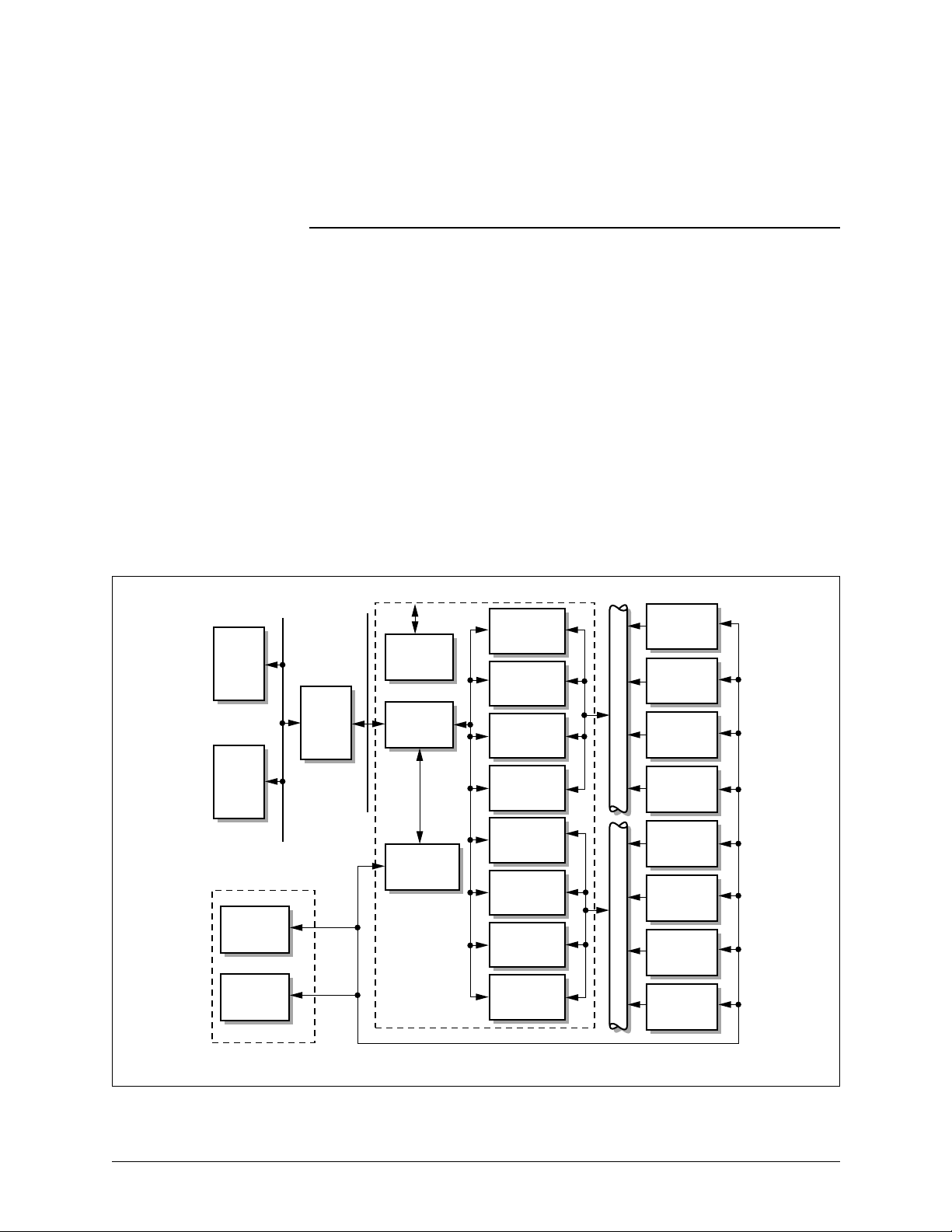
Access to MUSYCC is available through PCI read, write, and configuration cycles (see Figure 1-1).
Figure 1-1. System Block Diagram
System
Host
System
Memory
Optional
Components
Local
Host
Local
Memory
8478_001
Local Bus
Local
Bridge
Bus
PCI
PCI Bus
EBUS
JTAG
Host
Interface
(PCI)
Expansion
Bus
Interface
MUSYCC
Serial
Interface 0
Serial
Interface 1
Serial
Interface 2
Serial
Interface 3
Serial
Interface 4
Serial
Interface 5
Serial
Interface 6
Serial
Interface 7
Physical
Interface 0
Physical
Interface 1
Physical
Interface 2
PCM Highway(s)
Physical
Interface 3
Physical
Interface 4
Physical
Interface 5
Physical
Interface 6
PCM Highway( s)
Physical
Interface 7
100660E Conexant 1-1
Page 16

1.0 System Description CN8478/CN8474A/CN8472A/CN8471A
Multichannel Synchronous Communications Controller (MUSYCC™)
MUSYCC also provides an on-device, 32-bit local expansion bus (EBUS) controller which allows a host
processor to access local memory and physical interface devices directly through MUSYCC over the PCI using
configurable memory mapping features.
MUSYCC manages buffer memory for each active data channel with common list-processing structures.
The on-device features allow data transmission between buffer memory and the serial interfaces with minimum
host processor intervention. This allows the host processor to concentrate on managing the higher layers of the
protocol stack.
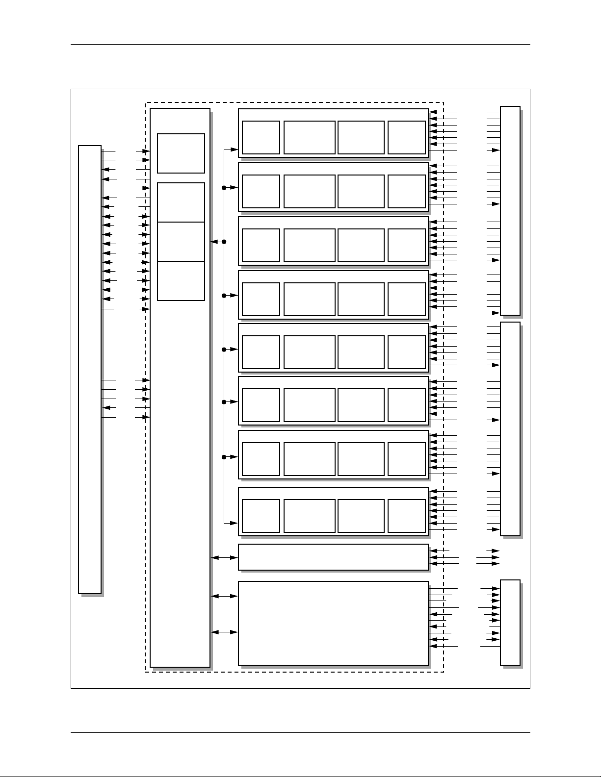
Figures 1-2 and 1-3 illustrate detailed system block diagrams and a sample application.
1-2 Conexant 100660E
Page 17
CN8478/CN8474A/CN8472A/CN8471A 1.0 System Description
Multichannel Synchronous Communications Controller (MUSYCC™)
Figure 1-2. Detailed System Block Diagram
PCLK
PRST*
INTB*
INTA*
GNT*
REQ*
SERR*
PERR*
IDSEL*
FRAME*
IRDY*
TRDY*
DEVSEL*
STOP*
PAR*
CBE[3:0]*
AD[31:0]
M66EN
PCI Bus
TCK
TEN*
3.3/5.0 Volt, 33/66 MHz
TMS
TDO
TDI
Host Interface
Device
Configuration
Registers
PCI
Interface
PCI
Configuration
Space
[Function 0]
PCI
Configuration
Space
[Function 1]
Interrupt
Controller
Interrupt
Controller
Interrupt
Controller
Interrupt
Controller
Interrupt
Controller
Interrupt
Controller
Interrupt
Controller
Serial Interface Channel Group 0
DMA
Controller
Tx/Rx-DMAC
Serial Interface Channel Group 1
DMA
Controller
Tx/Rx-DMAC
Serial Interface Channel Group 2
DMA
Controller
Tx/Rx-DMAC
Serial Interface Channel Group 3
DMA
Controller
Tx/Rx-DMAC
Serial Interface Channel Group 4
DMA
Controller
Tx/Rx-DMAC
Serial Interface Channel Group 5
DMA
Controller
Tx/Rx-DMAC
Serial Interface Channel Group 6
DMA
Controller
Tx/Rx-DMAC
Bit-Level
Processor
Tx/Rx-BLP
Bit-Level
Processor
Tx/Rx-BLP
Bit-Level
Processor
Tx/Rx-BLP
Bit-Level
Processor
Tx/Rx-BLP
Bit-Level
Processor
Tx/Rx-BLP
Bit-Level
Processor
Tx/Rx-BLP
Bit-Level
Processor
Tx/Rx-BLP
Port
Interface
Tx/Rx
Port
Interface
Tx/Rx
Port
Interface
Tx/Rx
Port
Interface
Tx/Rx
Port
Interface
Tx/Rx
Port
Interface
Tx/Rx
Port
Interface
Tx/Rx
RCLK0
RSYNC0
RDAT0
ROOF0
TCLK0
TSYNC0
TDAT0
RCLK1
RSYNC1
RDAT1
ROOF1
TCLK1
TSYNC1
TDAT1
RCLK2
RSYNC2
RDAT2
ROOF2
TCLK2
TSYNC2
TDAT2
RCLK3
RSYNC3
RDAT3
ROOF3
TCLK3
TSYNC3
TDAT3
RCLK4
RSYNC4
RDAT4
ROOF4
TCLK4
TSYNC4
TDAT4
RCLK5
RSYNC5
RDAT5
ROOF5
TCLK5
TSYNC5
TDAT5
RCLK6
RSYNC6
RDAT6
ROOF6
TCLK6
TSYNC6
TDAT6
Serial Interface System BusSerial Interface System Bus
RCLK7
RSYNC7
RDAT7
ROOF7
TCLK7
TSYNC7
TDAT7
SCAN_EN
TM0
TM1
ECLK
RD* (DS*)
WR* (R/WR*)
ALE*
BGACK*
HOLD (BR*)
HLDA (BG*)
EBE[3:0]*
EAD[31:0]*
EINT*
Bus
Microprocessor
8478_002
Scan
Data
Control
Interrupt
Controller
Serial Interface Channel Group 7
DMA
Controller
Tx/Rx-DMAC
Boundary Scan and Test Access
Expansion Bus Interface
Bit-Level
Processor
Tx/Rx-BLP
Port
Interface
Tx/Rx
100660E Conexant 1-3
Page 18
1.0 System Description CN8478/CN8474A/CN8472A/CN8471A
Multichannel Synchronous Communications Controller (MUSYCC™)
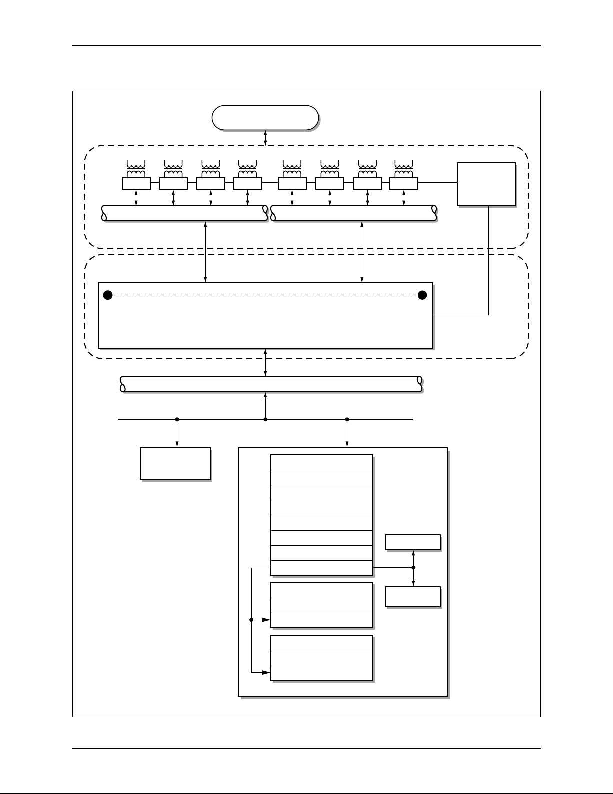
Figure 1-3. MUSYCC Application Example—Frame Relay Switch
Frame Relay Network
Control
PHY
PHY PHY PHY
PHY PHY
PHY
PHY
Data
MPU
(Optional)
System Bus – PCM Highway
Tx
Clk, Data,
Sync
Port 0
Ch Grp 0
Por t 1
Ch Grp 1
System Host
Clk, Data,
Sync, OOF
Port 2
Ch Grp 2
Rx
Physical Layer
Data Link Layer
Port 3
Ch Grp 3
Port 4
Ch Grp 4
Serial Port Interface
CN8478
Host Interface (PCI)
PCI Bus
PCI Local Bus Bridge
Channel Group 7 Descriptor
Channel Group 6 Descriptor
Channel Group 5 Descriptor
Channel Group 4 Descriptor
Channel Group 3 Descriptor
Channel Group 2 Descriptor
Channel Group 1 Descriptor
Channel Group 0 Descriptor
System Bus – PCM Highway
Tx
Clk, Data,
Sync
Port 5
Ch Grp 5
Ch Grp 6
Port 6
Rx
Clk, Data,
Sync, OOF
Por t 7
Ch Grp 7
Interface
Configuration
EBUS
32-Bit
Address
and Data
Multiplexed
EBUS
8478_003
Tx Channel 31 Message List
Tx Channel ... Message List
Tx Channel 0 Message List
Rx Channel 31 Message List
Rx Channel ... Message List
Rx Channel 0 Message List
System Memory
Interrupt
Queue
1-4 Conexant 100660E
Page 19
CN8478/CN8474A/CN8472A/CN8471A 1.0 System Description
Multichannel Synchronous Communications Controller (MUSYCC™)
1.1 Pin Descriptions
1.1 Pin Descriptions
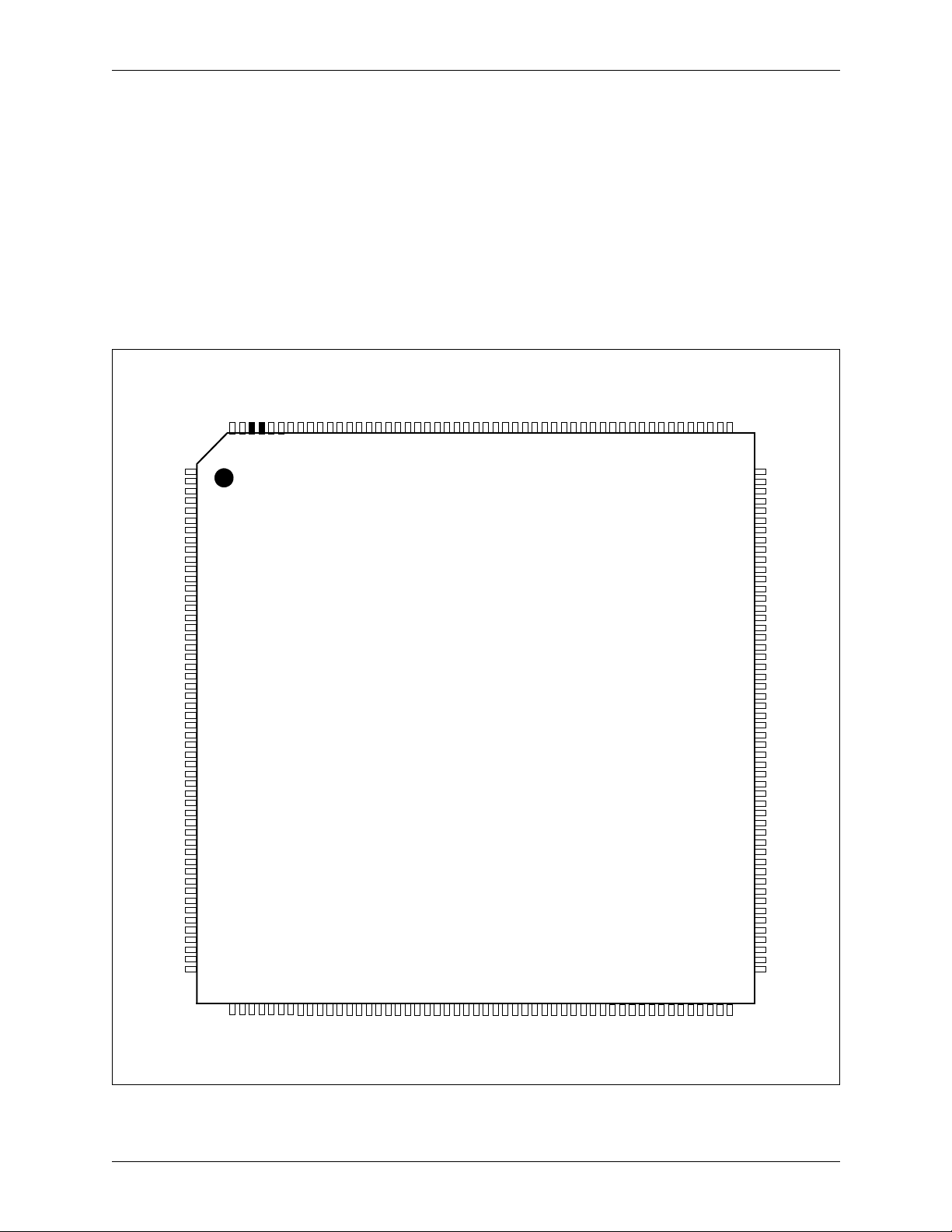
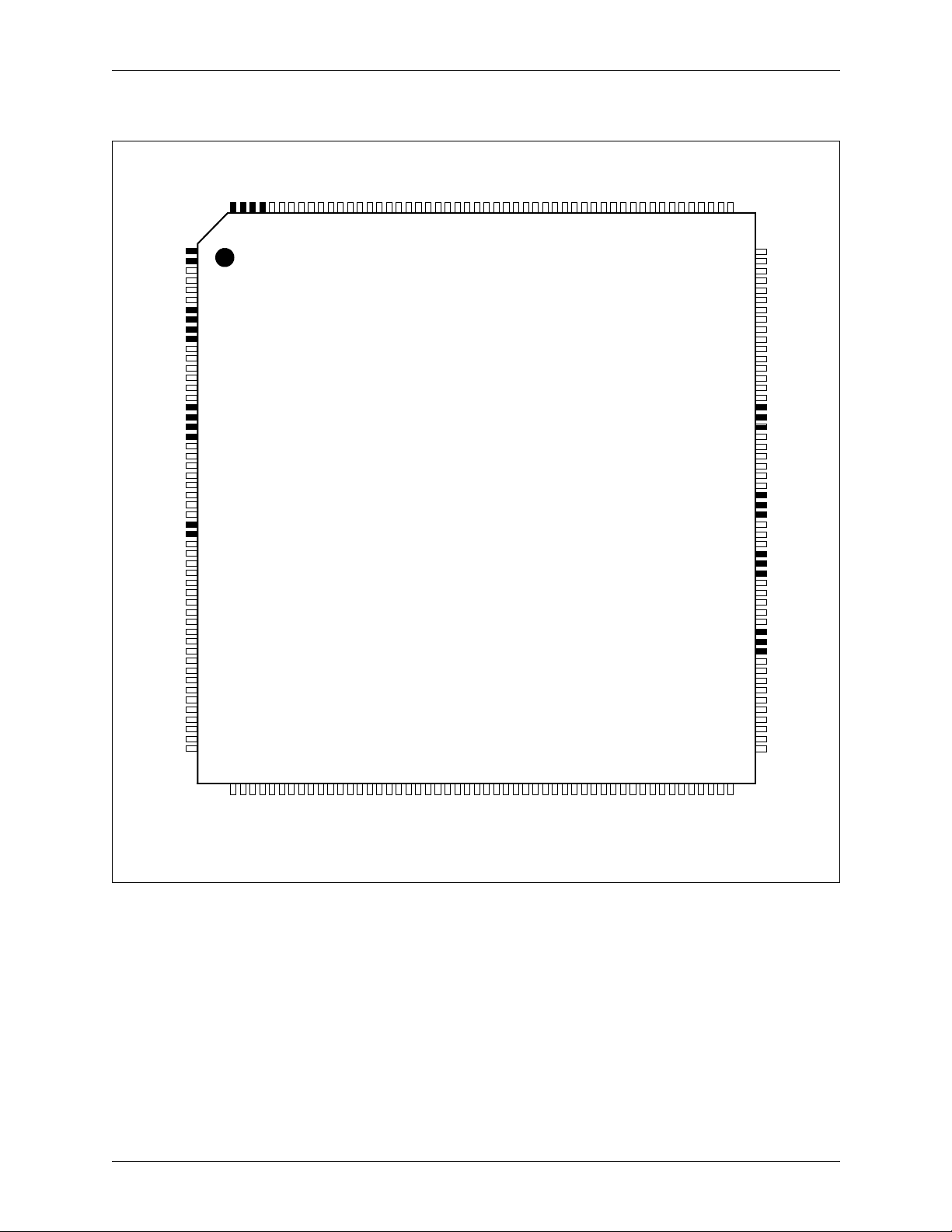
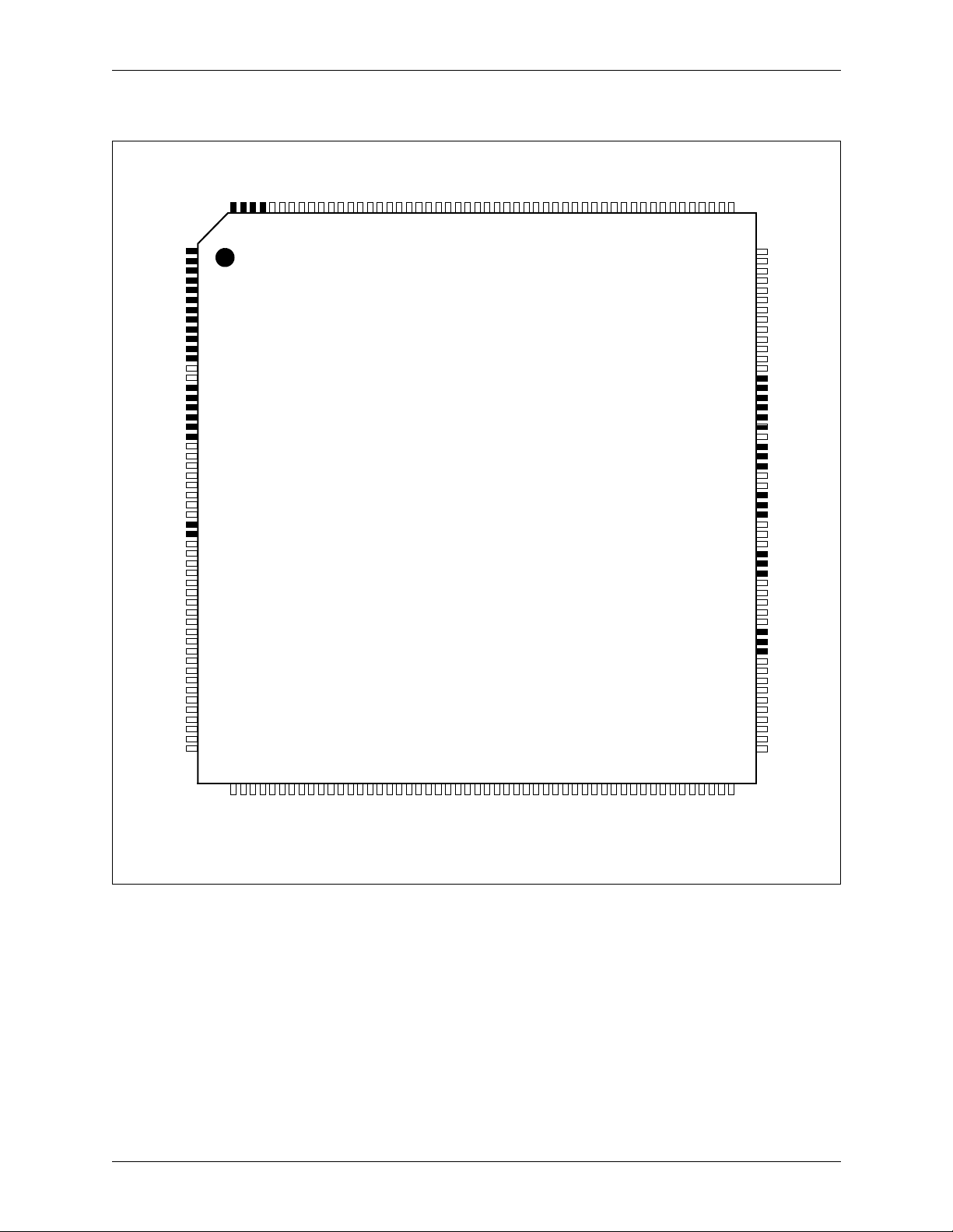
Figures 1-4 through 1-7 illustrate the pinouts for CN8478, CN8474A, CN8472A, and CN8471A. Signals
marked with black are NCs. Tables 1-1 and 1-2 summarize the pin assignments for the CN8478 in the MQFP
and PBGA packages, respectively. Ta ble 1 -3 lists the pin input and output functions. Table 1 -4 lists the hardware
signal definitions.
Figure 1-4. CN8478 MQFP Pinout Configuration
VDDc
EAD[30]
EAD[31]
189
VSS
EAD[29]
186
187
188
VDDo
VSSo
EAD[24]
EAD[25]
EAD[26]
EAD[27]
EAD[28]
181
182
183
184
185
EAD[22]
EAD[23]
176
177
178
179
180
Preliminary
CN8478
EAD[21]
VSSo
174
175
EAD[18]
169
EAD[17]
168
EAD[16]
167
EAD[15]
166
VSSo
165
VDDo
164
EAD[14]
163
EAD[13]
162
EAD[12]
161
EAD[11]
160
EAD[10]
159
VSS
EAD[9]
157
158
156
155
154
153
152
151
150
149
148
147
146
145
144
143
142
141
140
139
138
137
136
135
134
133
132
131
130
129
128
127
126
125
124
123
122
121
120
119
118
117
116
115
114
113
112
111
110
109
108
107
106
105
VGG
EAD[8]
EAD[7]
VSSo
EAD[6]
EAD[5]
EAD[4]
EAD[3]
VSSo
VDDo
EAD[2]
EAD[1]
EAD[0]
TCLK[3]
TSYNC[3]
TDAT[3]
TCLK[7]
TSYNC[7]
TDAT[7]
VSSo
TCLK[2]
TSYNC[2]
TDAT[2]
VSS
VDDc
TCLK[6]
TSYNC[6]
TDAT[6]
TCLK[1]
TSYNC[1]
TDAT[1]
TCLK[5]
TSYNC[5]
TDAT[5]
TCLK[0]
TSYNC[0]
TDAT[0]
VSS
VDDp
TCLK[4]
TSYNC[4]
TDAT[4]
TM[0]
TM[1]
TM[2]
VSSo
VDDo
AD[0]
AD[1]
AD[2]
AD[3]
AD[4]
EAD[19]
VDDp
EAD[20]
VSS
170
171
172
173
RSYNC[7]
RDAT[7]
ROOF[3]
RCLK[3]
RSYNC[3]
RDAT[3]
ROOF[6]
RCLK[6]
RSYNC[6]
RDAT[6]
ROOF[2]
RCLK[2]
VDDp
VSS
RSYNC[2]
RDAT[2]
ROOF[5]
RCLK[5]
RSYNC[5]
RDAT[5]
ROOF[1]
RCLK[1]
RSYNC[1]
RDAT[1]
ROOF[4]
RCLK[4]
VDDc
VSS
RSYNC[4]
RDAT[4]
ROOF[0]
RCLK[0]
RSYNC[0]
RDAT[0]
TCK
TRST*
TMS
TDO
TDI
INTB*
INTA*
VDDo
PCLK
VSSo
PRST
GNT*
REQ*
AD[31]
AD[30]
AD[29]
AD[28]
VGG
VDDo
VSSo
EBE[2]*
EBE[1]*
EBE[0]*NCNC
ROOF[7]
RCLK[7]
200
201
202
203
204
205
206
207
208
1
2
3
4
5
6
7
8
9
10
11
12
13
14
15
16
17
18
19
20
21
22
23
24
25
26
27
28
29
30
31
32
33
34
35
36
37
38
39
40
41
42
43
44
45
46
47
48
49
50
51
52
EINT*
HOLD(BR*)
HLDA(BG*)
BGACK*
EBE[3]*
195
196
197
198
199
ALE*(AS*)
194
ECLK
R*(R/WR*)
RD*(DS*)
VSSo
190
191
192
193
104
103
102
101
100
VSS
AD[27]
555453
VSSo
AD[26]
AD[25]
AD[24]
IDSEL
CBE[3]*
AD[23]
AD[22]
VSSo
VDDo
AD[21]
AD[20]
VSS
VDDp
AD[19]
AD[18]
AD[17]
AD[16]
VSSo
CBE[2]*
FRAME*
IRDY*
VDDc
VSS
TRDY*
DEVSEL*
VDDo
VSSo
STOP*
SERR*
PERR*
PAR
86858483828180797877767574737271706968676665646362616059585756
AD[15]
CBE[1]*
VSSo
AD[14]
AD[13]
AD[12]
AD[11]
AD[10]
VDDo
VSSo
AD[9]
99989796959493929190898887
AD[8]
M66EN
AD[7]
CBE[0]*
AD[5]
AD[6]
VSSo
100660E Conexant 1-5
Page 20

1.0 System Description CN8478/CN8474A/CN8472A/CN8471A
1.1 Pin Descriptions Multichannel Synchronous Communications Controller (MUSYCC™)
Table 1-1. CN8478 MQFP Pin List
Pin
Number
1 RSYNC[7]
2 RDAT[7]
3 ROOF[3]
4 RCLK[3]
5 RSYNC[3]
6 RDAT[3]
7 ROOF[6]
8 RCLK[6]
9 RSYNC[6]
10 RDAT[6]
11 ROOF[2]
12 RCLK[2]
13 VDDi
14 VSS
15 RSYNC[2]
16 RDAT[2]
17 ROOF[5]
18 RCLK[5]
19 RSYNC[5]
20 RDAT[5]
21 ROOF[1]
22 RCLK[1]
23 RSYNC[1]
24 RDAT[1]
25 ROOF[4]
26 RCLK[4]
27 VDDc
28 VSS
29 RSYNC[4]
30 RDAT[4]
31 ROOF[0]
32 RCLK[0]
33 RSYNC[0]
34 RDAT[0]
35 TCK
Pin Label
Pin
Number
36 TRST*
37 TMS
38 TDO
39 TDI
40 INTB*
41 INTA*
42 VDDo
43 PCLK
44 VSSo
45 PRST*
46 GNT*
47 REQ*
48 AD[31]
49 AD[30]
50 AD[29]
51 AD[28]
52 VGG
53 VSS
54 AD[27]
55 VSSo
56 AD[26]
57 AD[25]
58 AD[24]
59 CBE[3]*
60 IDSEL
61 AD[23]
62 AD[22]
63 VDDo
64 VSSo
65 AD[21]
66 AD[20]
67 VDDi
68 VSS
69 AD[19]
70 AD[18]
Pin Label
Pin
Number
71 AD[17]
72 AD[16]
73 VSSo
74 CBE[2]*
75 FRAME*
76 IRDY*
77 VDDc
78 VSS
79 TRDY*
80 DEVSEL*
81 VDDo
82 VSSo
83 STOP*
84 PERR*
85 SERR*
86 PAR
87 CBE[1]
88 AD[15]
89 VSSo
90 AD[14]
91 AD[13]
92 AD[12]
93 AD[11]
94 AD[10]
95 VDDo
96 VSSo
97 AD[9]
98 M66EN
99 AD[8]
100 CBE[0]*
101 AD[7]
102 AD[6]
103 AD[5]
104 VSSo
105 AD[4]
Pin Label
1-6 Conexant 100660E
Page 21

CN8478/CN8474A/CN8472A/CN8471A 1.0 System Description
Multichannel Synchronous Communications Controller (MUSYCC™)
Pin
Number
106 AD[3]
107 AD[2]
108 AD[1]
109 AD[0]
110 VDDo
111 VSSo
112 TM[2]
113 TM[1]
114 TM[0]
115 TDAT[4]
116 TSYNC[4]
117 TCLK[4]
118 VDDi
119 VSS
Pin Label
Pin
Number
142 TSYNC[3]
143 TCLK[3]
144 EAD[0]
145 EAD[1]
146 EAD[2]
147 VDDo
148 VSSo
149 EAD[3]
150 EAD[4]
151 EAD[5]
152 EAD[6]
153 VSSo
154 EAD[7]
155 EAD[8]
Pin Label
1.1 Pin Descriptions
Pin
Number
178 EAD[24]
179 EAD[25]
180 EAD[26]
181 VDDo
182 VSSo
183 EAD[27]
184 EAD[28]
185 VDDc
186 VSS
187 EAD[29]
188 EAD[30]
189 EAD[31]
190 ECLK
191 VSSo
Pin Label
120 TDAT[0]
121 TSYNC[0]
122 TCLK[0]
123 TDAT[5]
124 TSYNC[5]
125 TCLK[5]
126 TDAT[1]
127 TSYNC[1]
128 TCLK[1]
129 TDAT[6]
130 TSYNC[6]
131 TCLK[6]
132 VDDc
133 VSS
134 TDAT[2]
135 TSYNC[2]
136 TCLK[2]
137 VSSo
156 VGG
157 VSS
158 EAD[9]
159 EAD[10]
160 EAD[11]
161 EAD[12]
162 EAD[13]
163 EAD[14]
164 VDDo
165 VSSo
166 EAD[15]
167 EAD[16]
168 EAD[17]
169 EAD[18]
170 EAD[19]
171 VDDi
172 VSS
173 EAD[20]
192 WR*(R/ WR*)
193 RD*(DS*)
194 ALE*(AS*)
195 EINT*
196 HOLD(BR*)
197 HLDA(BG*)
198 BGACK*
199 EBE[3]*
200 EBE[2]*
201 VDDo
202 VSSo
203 EBE[1]*
204 EBE[0]*
205 NC
206 NC
207 ROOF[7]
208 RCLK[7]
138 TDAT[7]
139 TSYNC[7]
140 TCLK[7]
141 TDAT[3]
174 EAD[21]
175 VSSo
176 EAD[22]
177 EAD[23]
100660E Conexant 1-7
Page 22
1.0 System Description CN8478/CN8474A/CN8472A/CN8471A
1.1 Pin Descriptions Multichannel Synchronous Communications Controller (MUSYCC™)
Figure 1-5. CN8474A MPQF Pinout Configuration
ROOF[3]
RCLK[3]
RSYNC[3]
RDAT[3]
ROOF[2]
RCLK[2]
VDDp
VSS
RSYNC[2]
RDAT[2]
ROOF[1]
RCLK[1]
RSYNC[1]
RDAT[1]
VDDc
VSS
ROOF[0]
RCLK[0]
RSYNC[0]
RDAT[0]
TCK
TRST*
TMS
TDO
TDI
INTB*
INTA*
VDDo
PCLK
VSSo
PRST
GNT*
REQ*
AD[31]
AD[30]
AD[29]
AD[28]
VGG
161
EAD[12]
VSS
EAD[9]
EAD[10]
EAD[11]
157
158
159
160
156
VGG
155
EAD[8]
154
EAD[7]
153
VSSo
152
EAD[6]
151
EAD[5]
150
EAD[4]
149
EAD[3]
148
VSSo
147
VDDo
146
EAD[2]
145
EAD[1]
144
EAD[0]
143
TCLK[3]
142
TSYNC[3]
141
TDAT[3]
140
NC
139
NC
138
NC
137
VSSo
136
TCLK[2]
135
TSYNC[2]
134
TDAT[2]
133
VSS
132
VDDc
131
NC
130
NC
129
NC
TCLK[1]
128
TSYNC[1]
127
126
TDAT[1]
125
NC
124
NC
123
NC
122
TCLK[0]
121
TSYNC[0]
120
TDAT[0]
119
VSS
118
VDDp
117
NC
116
NC
115
NC
114
TM[0]
113
TM[1]
112
TM[2]
111
VSSo
110
VDDo
109
AD[0]
AD[1]
108
AD[2]
107
AD[3]
106
AD[4]
105
VDDc
VDDo
EBE[1]*
EBE[0]*NCNC
NC
NC
207
208
NC
1
NC
2
3
4
5
6
NC
7
NC
8
9
NC
NC
10
11
12
13
14
15
16
17
NC
NC
18
NC
19
NC
20
21
22
23
24
NC
25
NC
26
27
28
NC
29
NC
30
31
32
33
34
35
36
37
38
39
40
41
42
43
44
45
46
47
48
49
50
51
52
VSSo
201
202
203
204
205
206
HOLD(BR*)
HLDA(BG*)
BGACK*
EBE[3]*
EBE[2]*
196
197
198
199
200
VSSo
EAD[29]
EAD[30]
EAD[31]
ECLK
R*(R/WR*)
RD*(DS*)
ALE*(AS*)
EINT*
191
192
193
194
195
VSS
186
187
188
189
190
Preliminary
CN8474A
VDDo
VSSo
EAD[26]
EAD[27]
EAD[28]
180
181
182
183
184
185
EAD[25]
179
EAD[24]
178
EAD[23]
177
176
EAD[22]
VSSo
174
175
EAD[21]
EAD[19]
EAD[20]
VDDp
VSS
170
171
172
173
VSSo
EAD[13]
EAD[14]
EAD[15]
EAD[16]
EAD[17]
EAD[18]
169
VDDo
162
163
164
165
166
167
168
104
103
102
101
100
VSSo
VDDo
AD[9]
99989796959493929190898887
AD[8]
M66EN
AD[7]
CBE[0]*
AD[5]
AD[6]
VSSo
53
VSS
AD[27]
VSSo
AD[26]
AD[25]
AD[24]
IDSEL
CBE[3]*
AD[23]
AD[22]
VSSo
VDDo
AD[21]
AD[20]
VSS
VDDp
AD[19]
AD[18]
AD[17]
AD[16]
VSSo
CBE[2]*
FRAME*
IRDY*
VSS
VDDc
TRDY*
DEVSEL*
VSSo
VDDo
STOP*
SERR*
PERR*
PAR
868584838281807978777675747372717069686766656463626160595857565554
AD[15]
CBE[1]*
VSSo
AD[14]
AD[13]
AD[12]
AD[11]
AD[10]
NOTE(S): An active low signal is denoted by a trailing asterisk (*).
1-8 Conexant 100660E
Page 23
CN8478/CN8474A/CN8472A/CN8471A 1.0 System Description
Multichannel Synchronous Communications Controller (MUSYCC™)
Figure 1-6. CN8472A MQFP Pinout Configuration
VDDc
VDDo
VSSo
EAD[24]
EAD[25]
EAD[26]
EAD[27]
EAD[28]
178
179
180
181
182
183
184
185
NC
NC
NC
NC
NC
NC
NC
NC
NC
NC
NC
NC
VDDp
VSS
NC
NC
NC
NC
NC
NC
ROOF[1]
RCLK[1]
RSYNC[1]
RDAT[1]
NC
NC
VDDc
VSS
NC
NC
ROOF[0]
RCLK[0]
RSYNC[0]
RDAT[0]
TCK
TRST*
TMS
TDO
TDI
INTB*
INTA*
VDDo
PCLK
VSSo
PRST
GNT*
REQ*
AD[31]
AD[30]
AD[29]
AD[28]
VGG
VDDo
EBE[1]*
EBE[0]*NCNC
NC
NC
207
208
1
2
3
4
5
6
7
8
9
10
11
12
13
14
15
16
17
18
19
20
21
22
23
24
25
26
27
28
29
30
31
32
33
34
35
36
37
38
39
40
41
42
43
44
45
46
47
48
49
50
51
52
VSSo
201
202
203
204
205
206
HOLD(BR*)
HLDA(BG*)
BGACK*
EBE[3]*
EBE[2]*
196
197
198
199
200
VSSo
EAD[29]
EAD[30]
EAD[31]
ECLK
R*(R/WR*)
RD*(DS*)
ALE*(AS*)
EINT*
191
192
193
194
195
VSS
186
187
188
189
190
Preliminary
CN8472A
EAD[23]
177
176
EAD[22]
VSSo
174
175
EAD[21]
1.1 Pin Descriptions
161
EAD[12]
VSS
EAD[9]
EAD[10]
EAD[11]
157
158
159
160
156
VGG
155
EAD[8]
154
EAD[7]
153
VSSo
152
EAD[6]
151
EAD[5]
150
EAD[4]
149
EAD[3]
148
VSSo
147
VDDo
146
EAD[2]
145
EAD[1]
144
EAD[0]
143
NC
142
NC
141
NC
140
NC
139
NC
138
NC
137
VSSo
136
NC
135
NC
134
NC
133
VSS
132
VDDc
131
NC
130
NC
129
NC
TCLK[1]
128
TSYNC[1]
127
126
TDAT[1]
125
NC
124
NC
123
NC
122
TCLK[0]
121
TSYNC[0]
TDAT[0]
120
119
VSS
118
VDDp
117
NC
116
NC
115
NC
114
TM[0]
113
TM[1]
112
TM[2]
111
VSSo
110
VDDo
109
AD[0]
AD[1]
108
AD[2]
107
AD[3]
106
AD[4]
105
VDDp
VSS
169
170
171
172
173
VDDo
162
163
164
165
166
167
168
VSSo
EAD[13]
EAD[14]
EAD[15]
EAD[16]
EAD[17]
EAD[18]
EAD[19]
EAD[20]
104
103
102
101
100
VSSo
VDDo
AD[9]
99989796959493929190898887
AD[8]
M66EN
AD[7]
CBE[0]*
AD[5]
AD[6]
VSSo
53
VSS
AD[27]
VSSo
AD[26]
AD[25]
AD[24]
IDSEL
CBE[3]*
AD[23]
AD[22]
VSSo
VDDo
AD[21]
AD[20]
VSS
VDDp
AD[19]
AD[18]
AD[17]
AD[16]
VSSo
CBE[2]*
FRAME*
IRDY*
VSS
VDDc
TRDY*
DEVSEL*
VSSo
VDDo
STOP*
SERR*
PERR*
PAR
868584838281807978777675747372717069686766656463626160595857565554
AD[15]
CBE[1]*
VSSo
AD[14]
AD[13]
AD[12]
AD[11]
AD[10]
NOTE(S): An active low signal is denoted by a trailing asterisk (*).
100660E Conexant 1-9
Page 24
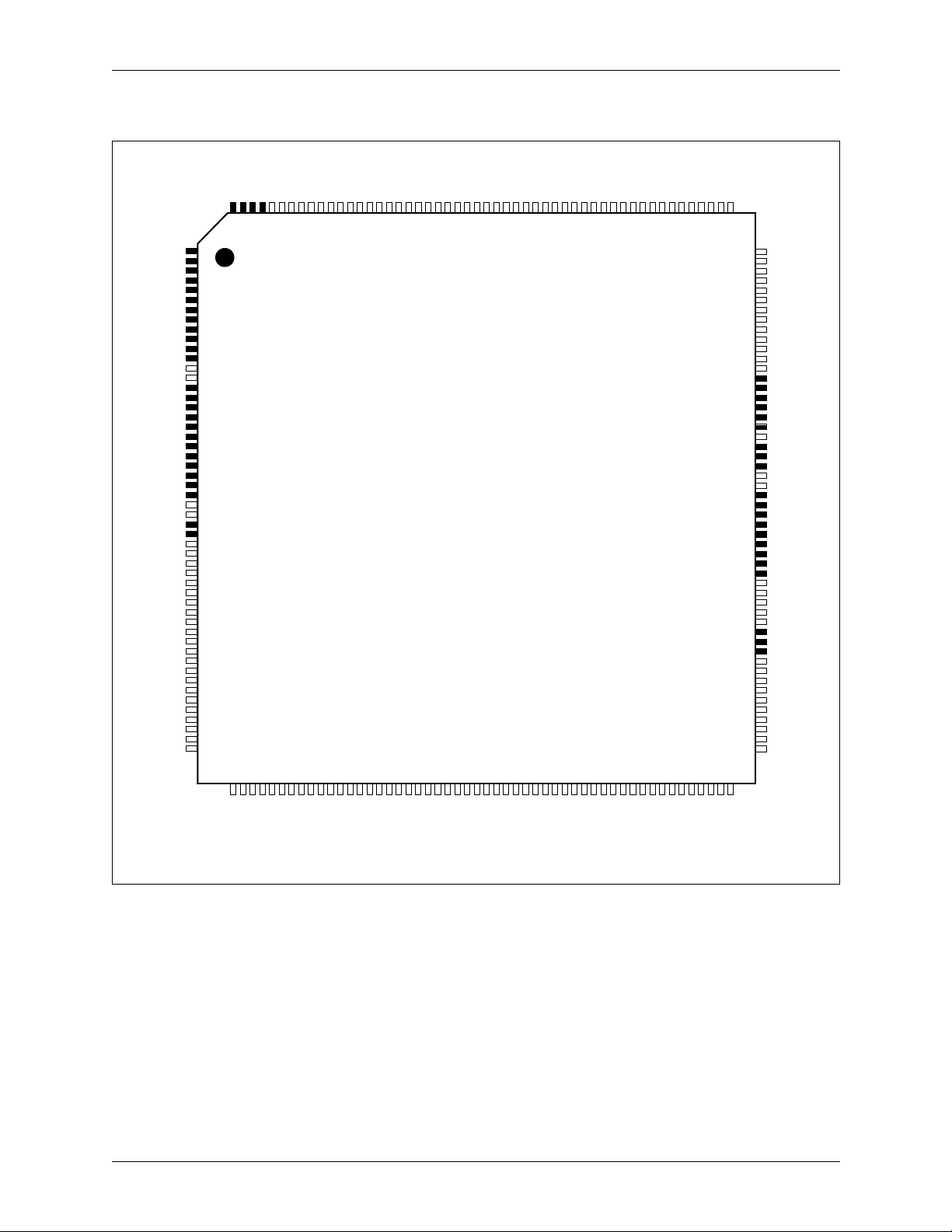
1.0 System Description CN8478/CN8474A/CN8472A/CN8471A
1.1 Pin Descriptions Multichannel Synchronous Communications Controller (MUSYCC™)
Figure 1-7. CN8471A MQFP Pinout Configuration
VDDp
VSS
VDDc
VSS
ROOF[0]
RCLK[0]
RSYNC[0]
RDAT[0]
TCK
TRST*
TMS
TDO
TDI
INTB*
INTA*
VDDo
PCLK
VSSo
PRST
GNT*
REQ*
AD[31]
AD[30]
AD[29]
AD[28]
VGG
VDDo
VSSo
EBE[1]*
EBE[0]*NCNC
NC
NC
201
202
203
204
205
206
207
208
NC
1
NC
2
NC
3
NC
4
NC
5
NC
6
NC
7
NC
8
9
NC
NC
10
NC
11
NC
12
13
14
NC
15
NC
16
17
NC
NC
18
NC
19
NC
20
NC
21
NC
22
NC
23
NC
24
NC
25
NC
26
27
28
NC
29
NC
30
31
32
33
34
35
36
37
38
39
40
41
42
43
44
45
46
47
48
49
50
51
52
HOLD(BR*)
HLDA(BG*)
BGACK*
EBE[3]*
EBE[2]*
195
196
197
198
199
200
ECLK
R*(R/WR*)
RD*(DS*)
ALE*(AS*)
EINT*
VSSo
190
191
192
193
194
VDDc
EAD[30]
EAD[31]
189
VSS
EAD[29]
186
187
188
VDDo
VSSo
EAD[24]
EAD[25]
EAD[26]
EAD[27]
EAD[28]
182
183
184
185
EAD[23]
176
177
178
179
180
181
Preliminary
CN8471A
EAD[22]
VSSo
174
175
EAD[21]
EAD[19]
VDDp
EAD[20]
VSS
170
171
172
173
VSSo
EAD[12]
EAD[13]
EAD[14]
EAD[15]
EAD[16]
EAD[17]
EAD[18]
169
VDDo
162
163
164
165
166
167
168
VSS
EAD[9]
EAD[11]
EAD[10]
157
158
159
160
161
156
VGG
155
EAD[8]
154
EAD[7]
153
VSSo
152
EAD[6]
151
EAD[5]
150
EAD[4]
149
EAD[3]
148
VSSo
147
VDDo
146
EAD[2]
145
EAD[1]
144
EAD[0]
143
NC
142
NC
141
NC
140
NC
139
NC
138
NC
137
VSSo
136
NC
135
NC
134
NC
133
VSS
132
VDDc
131
NC
130
NC
129
NC
NC
128
127
NC
126
NC
125
NC
124
NC
123
NC
122
TCLK[0]
121
TSYNC[0]
120
TDAT[0]
119
VSS
118
VDDp
117
NC
116
NC
115
NC
114
TM[0]
113
TM[1]
112
TM[2]
111
VSSo
110
VDDo
109
AD[0]
AD[1]
108
AD[2]
107
AD[3]
106
AD[4]
105
104
103
102
101
100
VSSo
VDDo
AD[9]
99989796959493929190898887
AD[8]
M66EN
AD[7]
CBE[0]*
AD[5]
AD[6]
VSSo
53
VSS
AD[27]
VSSo
AD[26]
AD[25]
AD[24]
IDSEL
CBE[3]*
AD[23]
AD[22]
VSSo
VDDo
AD[21]
AD[20]
VSS
VDDp
AD[19]
AD[18]
AD[17]
AD[16]
VSSo
CBE[2]*
FRAME*
IRDY*
VSS
VDDc
TRDY*
DEVSEL*
VSSo
VDDo
STOP*
SERR*
PERR*
PAR
868584838281807978777675747372717069686766656463626160595857565554
AD[15]
CBE[1]*
VSSo
AD[14]
AD[13]
AD[12]
AD[11]
AD[10]
NOTE(S): An active low signal is denoted by a trailing asterisk(*).
1-10 Conexant 100660E
Page 25
CN8478/CN8474A/CN8472A/CN8471A 1.0 System Description
Multichannel Synchronous Communications Controller (MUSYCC™)
Figure 1-8. CN8478 PBGA Pinout Configuration (Top View)
2 3 4 5 6 7 8 9 10 11 12 13 14 15 16
1
A
B
C
D
E
F
G
H
J
K
L
M
N
P
R
T
VSSo
RSYNC[7]
ROOF[3]
RDAT[3]
ROOF[2]
RDAT[2]
RDAT[5]
RSYNC[1]
ROOF[4]
RCLK[0]
RDAT[0]
INTA*
GNT*
AD[30]
AD[28]
VSSo
RCLK[7]
VSSo
RDAT[7]
RSYNC[3]
RSYNC[6]
RSYNC[2]
RCLK[5]
RCLK[1]
RCLK[4]
RDAT[4]
TCK
INTB*
PRST*
AD[31]
VSSo
VGG
ROOF[7]
NC
VSSo
RCLK[3]
RCLK[6]
RCLK[2]
ROOF[5]
RSYNC[5]
ROOF[1]
RDAT[1]
RSYNC[4]
RSYNC[0]
TDO
PCLK
VSSo
AD[29]
AD[27]
NC
EBE[0]*
EBE[1]*
VSSo
RDAT[6]
VDDi
VDDc
ROOF[0]
TRST*
TMS
VDDo
VSSo
REQ*
AD[26]
AD[25]
EBE[2]*
HOLD(BR*)
HLDA(BG*)
WR*(R/WR*)
EBE[3]*
ROOF[6]
TDI
AD[24]
CBE[3]*
IDSEL
EINT*
VDDo
VDDi
AD[23]
AD[21]
AD[22]
ECLK
EAD[30]
ALE*(AS*)
BGACK*
VSS
VSS
VSS
VSS
AD[17]
AD[20]
AD[19]
AD[18]
EAD[27]
EAD[29]
EAD[24]
EAD[28]
EAD[26]
RD*(DS*)
VDDc
EAD[31]
CN8478
VSS
VSS
VSS
VSS VSS
VSS
VSS
VSS
VSS VSS
PAR
VDDc
IRDY*
AD[16]
TRDY*
CBE[2]*
DEVSEL*
FRAME*
EAD[23]
EAD[21]
EAD[22]
EAD[25]
VSS
VSS
AD[13]
PERR*
STOP*
SERR*
EAD[20]
EAD[17]
EAD[19]
VDDi
VDDo
AD[15]
CBE[1]
AD[14]
EAD[18]
EAD[14]
EAD[13]
EAD[15]
AD[8]
AD[11]
AD[12]
AD[10]
EAD[16]
EAD[11]
EAD[6]
VSSo
EAD[1]
VDDo
TSYNC[7]
VDDc
TCLK[1]
TCLK[5]
VDDi
TSYNC[4]
VSSo
M66EN
AD[9]
CBE[0]*
EAD[12]
EAD[9]
VSSo
EAD[4]
TCLK[3]
TDAT[3]
TCLK[2]
TSYNC[6]
TDAT[1]
TCLK[0]
TDAT[0]
TM[0]
AD[1]
VSSo
AD[7]
AD[6]
EAD[10]
VSSo
EAD[7]
EAD[3]
EAD[0]
TCLK[7]
TSYNC[2]
TCLK[6]
TSYNC[1]
TDAT[5]
TCLK[4]
TM[1]
AD[0]
AD[3]
VSSo
AD[5]
1.1 Pin Descriptions
VSSo
VGG
EAD[8]
EAD[5]
EAD[2]
TSYNC[3]
TDAT[7]
TDAT[2]
TDAT[6]
TSYNC[5]
TSYNC[0]
TDAT[4]
TM[2]
AD[2]
AD[4]
VSSo
8478_044
100660E Conexant 1-11
Page 26

1.0 System Description CN8478/CN8474A/CN8472A/CN8471A
1.1 Pin Descriptions Multichannel Synchronous Communications Controller (MUSYCC™)
Table 1-2. CN8478 PBGA Pin List
Pin
Number
A1 VSSo
A2 RCLK[7]
A3 ROOF[7]
A4 NC
A5 EBE[2]*
A6 HOLD(BR*)
A7 ECLK
A8 EAD[29]
A9 EAD[27]
A10 EAD[23]
A11 EAD[20]
A12 EAD[18]
A13 EAD[16]
A14 EAD[12]
A15 EAD[10]
A16 VSSo
B1 RSYNC[7]
B2 VSSo
B3 NC
B4 EBE[0]*
B5 HLDA(BG*)
B6 WR*(R/ WR*)
B7 EAD[30]
B8 EAD[28]
B9 EAD[24]
B10 EAD[21]
B11 EAD[17]
B12 EAD[14]
B13 EAD[11]
B14 EAD[9]
B15 VSSo
B16 VGG
C1 ROOF[3]
C2 RDAT[7]
C3 VSSo
Pin Label
Pin
Number
C4 EBE[1]*
C5 EBE[3]*
C6 EINT*
C7 ALE*(AS*)
C8 RD*(DS*)
C9 EAD[26]
C10 EAD[22]
C11 EAD[19]
C12 EAD[13]
C13 EAD[6]
C14 VSSo
C15 EAD[7]
C16 EAD[8]
D1 RDAT[3]
D2 RSYNC[3]
D3 RCLK[3]
D4 VSSo
D5 ROOF[6]
D6 VDDo
D7 BGACK*
D8 EAD[31]
D9 VDDc
D10 EAD[25]
D11 VDDi
D12 EAD[15]
D13 VSSo
D14 EAD[4]
D15 EAD[3]
D16 EAD[5]
E1 ROOF[2]
E2 RSYNC[6]
E3 RCLK[6]
E4 RDAT[6]
E13 EAD[1]
E14 TCLK[3]
Pin Label
Pin
Number
E15 EAD[0]
E16 EAD[2]
F1 RDAT[2]
F2 RSYNC[2]
F3 RCLK[2]
F4 VDDi
F13 VDDo
F14 TDAT[3]
F15 TCLK[7]
F16 TSYNC[3]
G1 RDAT[5]
G2 RCLK[5]
G3 ROOF[5]
G4 RSYNC[5]
G7 VSS
G8 VSS
G9 VSS
G10 VSS
G13 TSYNC[7]
G14 TCLK[2]
G15 TSYNC[2]
G16 TDAT[7]
H1 RSYNC[1]
H2 RCLK[1]
H3 ROOF[1]
H4 VDDc
H7 VSS
H8 VSS
H9 VSS
H10 VSS
H13 VDDc
H14 TSYNC[6]
H15 TCLK[6]
H16 TDAT[2]
J1 ROOF[4]
Pin Label
1-12 Conexant 100660E
Page 27

CN8478/CN8474A/CN8472A/CN8471A 1.0 System Description
Multichannel Synchronous Communications Controller (MUSYCC™)
Pin
Number
J2 RCLK[4]
J3 RDAT[1]
J4 ROOF[0]
J7 VSS
J8 VSS
J9 VSS
J10 VSS
J13 TCLK[1]
J14 TDAT[1]
J15 TSYNC[1]
J16 TDAT[6]
K1 RCLK[0]
K2 RDAT[4]
K3 RSYNC[4]
K4 TRST*
Pin Label
Pin
Number
M14 TM[0]
M15 TM[1]
M16 TDAT[4]
N1 GNT*
N2 PRST*
N3 PCLK
N4 VSSo
N5 TDI
N6 VDDi
N7 AD[17]
N8 VDDc
N9 PAR
N10 AD[13]
N11 VDDo
N12 AD[8]
Pin Label
Pin
Number
R2 VSSo
R3 AD[29]
R4 AD[26]
R5 CBE[3]*
R6 AD[21]
R7 AD[19]
R8 CBE[2]*
R9 TRDY*
R10 STOP*
R11 CBE[1]
R12 AD[12]
R13 AD[9]
R14 AD[7]
R15 VSSo
R16 AD[4]
Pin Label
1.1 Pin Descriptions
K7 VSS
K8 VSS
K9 VSS
K10 VSS
K13 TCLK[5]
K14 TCLK[0]
K15 TDAT[5]
K16 TSYNC[5]
L1 RDAT[0]
L2 TCK
L3 RSYNC[0]
L4 TMS
L13 VDDi
L14 TDAT[0]
L15 TCLK[4]
L16 TSYNC[0]
M1 INTA*
M2 INTB*
N13 VSSo
N14 AD[1]
N15 AD[0]
N16 TM[2]
P1 AD[30]
P2 AD[31]
P3 VSSo
P4 REQ*
P5 AD[24]
P6 AD[23]
P7 AD[20]
P8 AD[16]
P9 IRDY*
P10 PERR*
P11 AD[15]
P12 AD[11]
P13 M66EN
P14 VSSo
T1 VSSo
T2 VGG
T3 AD[27]
T4 AD[25]
T5 IDSEL
T6 AD[22]
T7 AD[18]
T8 FRAME*
T9 DEVSEL*
T10 SERR*
T11 AD[14]
T12 AD[10]
T13 CBE[0]*
T14 AD[6]
T15 AD[5]
T16 VSSo
M3 TDO
M4 VDDo
M13 TSYNC[4]
P15 AD[3]
P16 AD[2]
R1 AD[28]
100660E Conexant 1-13
Page 28

1.0 System Description CN8478/CN8474A/CN8472A/CN8471A
1.1 Pin Descriptions Multichannel Synchronous Communications Controller (MUSYCC™)
Figure 1-9. CN8474A PBGA Pinout Configuration (Top View)
2 3 4 5 6 7 8 9 10 11 12 13 14 15 16
1
A
B
C
D
E
F
G
H
J
K
L
M
N
P
R
T
VSSo
NC
ROOF[3]
RDAT[3]
RSYNC[3]
ROOF[2]
RDAT[2]
RSYNC[2]
NC
RSYNC[1]
NC
RCLK[0]
RDAT[0]
INTA*
GNT*
AD[30]
AD[28]
VSSo
NC
VSSo
NC
NC
NC
RCLK[1]
NC
NC
TCK
INTB*
PRST*
AD[31]
VSSo
VGG
NC
NC
VSSo
RCLK[3]
NC
RCLK[2]
NC
ROOF[1]
RDAT[1]
NC
RSYNC[0]
TDO
PCLK
VSSo
AD[29]
AD[27]
NC
EBE[0]*
EBE[1]*
VSSo
NC
VDDi
NC
VDDc
ROOF[0]
TRST*
TMS
VDDo
VSSo
REQ*
AD[26]
AD[25]
EBE[2]*
HOLD(BR*)
HLDA(BG*)
WR*(R/WR*)
EBE[3]*
NC
TDI
AD[24]
CBE[3]*
IDSEL
EINT*
VDDo
VDDi
AD[23]
AD[21]
AD[22]
ECLK
EAD[30]
ALE*(AS*)
BGACK*
VSS
VSS
VSS
VSS
AD[17]
AD[20]
AD[19]
AD[18]
EAD[27]
EAD[29]
EAD[24]
EAD[28]
EAD[26]
RD*(DS*)
VDDc
EAD[31]
CN8474A
VSS
VSS
VSS
VSS VSS
VSS
VSS
VSS
VSS VSS
PAR
VDDc
IRDY*
AD[16]
TRDY*
CBE[2]*
DEVSEL*
FRAME*
EAD[23]
EAD[21]
EAD[22]
EAD[25]
VSS
VSS
AD[13]
PERR*
STOP*
SERR*
EAD[20]
EAD[17]
EAD[19]
VDDi
VDDo
AD[15]
CBE[1]
AD[14]
EAD[18]
EAD[14]
EAD[13]
EAD[15]
AD[8]
AD[11]
AD[12]
AD[10]
EAD[16]
EAD[11]
EAD[6]
VSSo
EAD[1]
VDDo
NC
VDDc
TCLK[1]
NC
VDDi
NC
VSSo
M66EN
AD[9]
CBE[0]*
EAD[12]
EAD[9]
VSSo
EAD[4]
TCLK[3]
TDAT[3]
TCLK[2]
NC
TDAT[1]
TCLK[0]
TDAT[0]
TM[0]
AD[1]
VSSo
AD[7]
AD[6]
EAD[10]
VSSo
EAD[7]
EAD[3]
EAD[0]
NC
TSYNC[3]
TSYNC[2]
NC
TSYNC[1]
NC
NC
TSYNC[0]
TM[1]
AD[0]
AD[3]
VSSo
AD[5]
VSSo
VGG
EAD[8]
EAD[5]
EAD[2]
NC
TDAT[2]
NC
NC
NC
TM[2]
AD[2]
AD[4]
VSSo
8478_045
1-14 Conexant 100660E
Page 29
CN8478/CN8474A/CN8472A/CN8471A 1.0 System Description
Multichannel Synchronous Communications Controller (MUSYCC™)
Figure 1-10. CN8472A PBGA Pinout Configuration (Top View)
2 3 4 5 6 7 8 9 10 11 12 13 14 15 16
1
A
B
C
D
E
F
G
H
J
K
L
M
N
P
R
T
VSSo
NC
NC
NC
NC
NC
NC
RSYNC[1]
NC
RCLK[0]
RDAT[0]
INTA*
GNT*
AD[30]
AD[28]
VSSo
NC
VSSo
NC
NC
NC
NC
NC
RCLK[1]
NC
NC
TCK
INTB*
PRST*
AD[31]
VSSo
VGG
NC
NC
VSSo
NC
NC
NC
NC
ROOF[1]
RDAT[1]
NC
RSYNC[0]
TDO
PCLK
VSSo
AD[29]
AD[27]
NC
EBE[0]*
EBE[1]*
VSSo
NC
VDDi
NC
VDDc
ROOF[0]
TRST*
TMS
VDDo
VSSo
REQ*
AD[26]
AD[25]
EBE[2]*
HOLD(BR*)
HLDA(BG)*
WR*(R/WR*)
EBE[3]*
NC
TDI
AD[24]
CBE[3]*
IDSEL
EINT*
VDDo
VDDi
AD[23]
AD[21]
AD[22]
ECLK
EAD[30]
ALE*(AS*)
BGACK*
VSS
VSS
VSS
VSS
AD[17]
AD[20]
AD[19]
AD[18]
EAD[27]
EAD[29]
EAD[24]
EAD[28]
EAD[26]
RD*(DS*)
VDDc
EAD[31]
CN8472A
VSS
VSS
VSS
VSS VSS
VSS
VSS
VSS
VSS VSS
PAR
VDDc
IRDY*
AD[16]
TRDY*
CBE[2]*
DEVSEL*
FRAME*
EAD[23]
EAD[21]
EAD[22]
EAD[25]
VSS
VSS
AD[13]
PERR*
STOP*
SERR*
EAD[20]
EAD[17]
EAD[19]
AD[15]
CBE[1]
AD[14]
VDDi
VDDo
EAD[18]
EAD[14]
EAD[13]
EAD[15]
AD[8]
AD[11]
AD[12]
AD[10]
EAD[16]
EAD[11]
EAD[6]
VSSo
EAD[1]
VDDo
NC
VDDc
TCLK[1]
NC
VDDi
NC
VSSo
M66EN
AD[9]
CBE[0]*
EAD[12]
EAD[9]
VSSo
EAD[4]
NC
NC
NC
NC
TDAT[1]
TCLK[0]
TDAT[0]
TM[0]
AD[1]
VSSo
AD[7]
AD[6]
EAD[10]
VSSo
EAD[7]
EAD[3]
EAD[0]
NC
NC
NC
TSYNC[1]
NC
NC
TSYNC[0]
TM[1]
AD[0]
AD[3]
VSSo
AD[5]
1.1 Pin Descriptions
VSSo
VGG
EAD[8]
EAD[5]
EAD[2]
NC
NC
NC
NC
NC
NC
TM[2]
AD[2]
AD[4]
VSSo
8478_046
100660E Conexant 1-15
Page 30

1.0 System Description CN8478/CN8474A/CN8472A/CN8471A
1.1 Pin Descriptions Multichannel Synchronous Communications Controller (MUSYCC™)
Figure 1-11. CN8471A PBGA Pinout Configuration (Top View)
2 3 4 5 6 7 8 9 10 11 12 13 14 15 16
1
VSSo
A
NC
B
NC
C
NC
D
NC
E
NC
F
NC
G
NC
H
NC
J
RCLK[0]
K
RDAT[0]
L
INTA*
M
GNT*
N
AD[30]
P
AD[28]
R
VSSo
T
NC
VSSo
NC
NC
NC
NC
NC
NC
NC
NC
TCK
INTB*
PRST*
AD[31]
VSSo
VGG
NC
NC
VSSo
NC
NC
NC
NC
NC
NC
NC
RSYNC[0]
TDO
PCLK
VSSo
AD[29]
AD[27]
NC
EBE[0]*
EBE[1]*
VSSo
NC
VDDi
NC
VDDc
ROOF[0]
TRST*
TMS
VDDo
VSSo
REQ*
AD[26]
AD[25]
EBE[2]*
HOLD(BR*)
HLDA(BG*)
WR*(R/WR*)
EBE[3]*
NC
TDI
AD[24]
CBE[3]*
IDSEL
EINT*
VDDo
VDDi
AD[23]
AD[21]
AD[22]
ECLK
EAD[30]
ALE*(AS*)
BGACK*
VSS
VSS
VSS
VSS
AD[17]
AD[20]
AD[19]
AD[18]
EAD[27]
EAD[29]
EAD[24]
EAD[28]
EAD[26]
RD*(DS*)
VDDc
EAD[31]
CN8471A
VSS
VSS
VSS
VSS VSS
VSS
VSS
VSS
VSS VSS
PAR
VDDc
IRDY*
AD[16]
TRDY*
CBE[2]*
DEVSEL*
FRAME*
EAD[23]
EAD[21]
EAD[22]
EAD[25]
VSS
VSS
AD[13]
PERR*
STOP*
SERR*
EAD[20]
EAD[17]
EAD[19]
VDDi
VDDo
AD[15]
CBE[1]
AD[14]
EAD[18]
EAD[14]
EAD[13]
EAD[15]
AD[8]
AD[11]
AD[12]
AD[10]
EAD[16]
EAD[11]
EAD[6]
VSSo
EAD[1]
VDDo
NC
VDDc
NC
NC
VDDi
NC
VSSo
M66EN
AD[9]
CBE[0]*
EAD[12]
EAD[9]
VSSo
EAD[4]
NC
NC
NC
NC
NC
TCLK[0]
TDAT[0]
TM[0]
AD[1]
VSSo
AD[7]
AD[6]
EAD[10]
VSSo
EAD[7]
EAD[3]
EAD[0]
NC
NC
NC
NC
NC
NC
TM[1]
AD[0]
AD[3]
VSSo
AD[5]
VSSo
VGG
EAD[8]
EAD[5]
EAD[2]
NC
NC
NC
NC
NC
TSYNC[0]
NC
TM[2]
AD[2]
AD[4]
VSSo
8478_047
1-16 Conexant 100660E
Page 31

CN8478/CN8474A/CN8472A/CN8471A 1.0 System Description
Multichannel Synchronous Communications Controller (MUSYCC™)
Figure 1-12. CN8478 Logic Diagram
198
Bus Grant Acknowledge
Hold Acknowledge
Hold Request
Expansion Bus Interrupt
Address Latch Enable
Read Strobe
Write Strobe/Read
Out-Of-Frame
Synchronization
Out-Of-Frame
Synchronization
Out-Of-Frame
Synchronization
Out-Of-Frame
Synchronization
Out-Of-Frame
Synchronization
Out-Of-Frame
Synchronization
Out-Of-Frame
Synchronization
Out-Of-Frame
Synchronization
JTAG Clock
JTAG Reset
JTAG Mode Select
JTAG Data Out
JTAG Data In
Initialization Device Select
Initiator Ready
Target Ready
Device Select
Parity Error
478_004
Clock
Data
Clock
Data
Clock
Data
Clock
Data
Clock
Data
Clock
Data
Clock
Data
Clock
Data
Clock
Reset
Grant
Frame
Stop
Parity
I/O
I/O
I/O
I/O
I/O
I/O
I/O
I/O
I
O
I
O
O
O
I
I
I
I
I
I
I
I
I
I
I
I
I
I
I
I
I
I
I
I
I
I
I
I
I
I
I
I
I
I
I
I
I
I
I
O
I
I
I
I
I
I
197
196
195
194
193
192
207
208
10
17
18
19
20
25
26
29
30
11
12
15
16
21
22
23
24
31
32
33
34
35
36
37
38
39
43
45
46
60
75
76
79
80
83
84
86
(3)
98
1
2
7
8
9
3
4
5
6
BGACK*
HLDA (BG*)
HOLD (BR*)
EINT*
ALE* (AS*)
RD* (DS*)
WR* (R/WR*)
ROOF[7]
RCLK[7]
RSYNC[7]
RDAT[7]
ROOF[6]
RCLK[6]
RSYNC[6]
RDAT[6]
ROOF[5]
RCLK[5]
RSYNC[5]
RDAT5]
ROOF[4]
RCLK[4]
RSYNC[4]
RDAT[4]
ROOF[3]
RCLK[3]
RSYNC[3]
RDAT[3]
ROOF[2]
RCLK[2]
RSYNC[2]
RDAT[2]
ROOF[1]
RCLK[1]
RSYNC[1]
RDAT[1]
ROOF[0]
RCLK[0]
RSYNC[0]
RDAT[0]
TCK
TRST*
TMS
TDO
TDI
PCLK
PRST*
GNT*
IDSEL
FRAME*
IRDY*
TRDY*
DEVSEL*
STOP*
PERR*
PAR
AD[31:0]Address and Data Bus I/O
M66ENM66EN
Expansion Bus
Interface
Serial Interface
Receive Serial
Channel Group
7
Receive Serial
Channel Group
6
Receive Serial
Channel Group
5
Receive Serial
Channel Group
4
Receive Serial
Channel Group
3
Receive Serial
Channel Group
2
Receive Serial
Channel Group
1
Receive Serial
Channel Group
0
Boundary Scan
Test Signal
Host (PCI)
Interface
Transmit Ser ial
Channel Group
7
Transmit Serial
Channel Group
6
Transmit Serial
Channel Group
5
Transmit Serial
Channel Group
4
Transmit Serial
Channel Group
3
Transmit Serial
Channel Group
2
Transmit Serial
Channel Group
1
Transmit Serial
Channel Group
0
Scan Chain
Test Access
190
ECLK
EBE[3:0]*
EAD[31:0]
TCLK[7]
TSYNC[7]
TDAT[7]
TCLK[6]
TSYNC[6]
TDAT[6]
TCLK[5]
TSYNC[5]
TDAT[5]
TCLK[4]
TSYNC[4]
TDAT[4]
TCLK[3]
TSYNC[3]
TDAT[3]
TCLK[2]
TSYNC[2]
TDAT[2]
TCLK[1]
TSYNC[1]
TDAT[1]
TCLK[0]
TSYNC[0]
TDAT[0]
CBE[3:0]*
140
149
138
131
130
129
125
124
123
117
116
115
143
142
141
136
135
134
128
127
126
122
121
120
114
TM[0]
113
TM[1]
112
TM[2]
INTB* PCI Interrupt BO
INTA* PCI Interrupt AO
REQ* RequestO
SERR* System ErrorO
1.1 Pin Descriptions
O
(1)
(2)
40
41
(4)
47
85
Clock
O
Expansion Bus Byte Enable
I/O
Expansion Bus Address/Data
I
Clock
I
Synchronization
O
Data
Clock
I
Synchronization
I
Data
O
Clock
I
Synchronization
I
Data
O
Clock
I
Synchronization
I
Data
O
Clock
I
Synchronization
I
Data
O
Clock
I
Synchronization
I
Data
O
Clock
I
Synchronization
I
Data
O
Clock
I
Synchronization
I
Data
O
I
Scan Enable
I
Scan Mode Bit 1
I
Scan Mode Bit 2
O
Command and Byte Enables
NOTE(S):
(1)
EBE [3:0]* pin numbers are 199-200, 203-204.
(2)
EAD [31:0] pin numbers are 144-146, 149-152, 145-155, 158-163, 166-170, 173-174, 176-180, 183-184, 187-189.
(3)
AD [31:0] pin numbers are 48-51, 54, 56-58, 61-62, 65-66, 69-72, 88, 90-94, 97, 99, 101-103, 105-109.
(4)
CBS [3.0]* pin numbers are 59, 74, 87,100.
(5)
An active low signal is denoted by a trailing asterisk (*).
100660E Conexant 1-17
Page 32

1.0 System Description CN8478/CN8474A/CN8472A/CN8471A
1.1 Pin Descriptions Multichannel Synchronous Communications Controller (MUSYCC™)
Table 1-3. I/O Pin Types
I/O Definition
I Input. High impedance, TTL.
OOutput. CMOS.
I/O Input/Output. TTL input/CMOS output.
t/s Three-state. Bidirectional three-state I/O pin.
s/t/s Sustained three-state. This is an active-low, three-state signal owned by only one driver at a time. The driver
that drives an s/t/s signal low must drive it high for at least one clock cycle before allowing it to float. A pullup
is required to sustain the deaserted value.
o/d Open drain.
NOTE(S): All outputs are CMOS drive levels and can be used with CMOS or TTL logic.
1-18 Conexant 100660E
Page 33

CN8478/CN8474A/CN8472A/CN8471A 1.0 System Description
Multichannel Synchronous Communications Controller (MUSYCC™)
1.1 Pin Descriptions
Table 1-4. CN8478 Hardware Signal Definitions (1 of 6)
MQFP
Pin No.
190 ECLK Expansion Bus Clock t/s O ECLK is an inverted version of the PCI clock applied at the PCLK
144-146,
149-152,
154-155,
158-163,
166-170,
173-174,
176-180,
183-184,
187-189
199, 200,
203, 204
Pin Label Signal Name I/O Definition
input.
EAD[31:0] Expansion Bus
Address and Data
EBE[3:0]* Expansion Bus
Byte Enables
t/s I/O EAD[31:0] is a multiplexed address/data bus. During the address
phase, pins EAD[17:0] contains meaningful address information.
It is the same address as PCI AD[19:2] for the corresponding
cycle.
Pins EAD[31:18] are driven to 0 during the address phase.
This is because those upper bits are compared, during the PCI
address phase, to the value in the relocatable EBUS Base
Address register to determine if the PCI cycle is in fact
addressing into MUSYCC EBUS space.
During data phase of an EBUS access cycle, the PCI signals
AD[31:0] are transferred to the EBUS signal lines EAD[31:0]
unaltered.
t/s O EBE* contains the same information as the PCI byte enables but
is driven in chip select style protocol used as active-low chip
selects when MUSYCC is connected to more than one byte-wide
device. All PCI accesses with byte lane 0’s byte enable asserted
would go to the byte-wide device connected to EAD[7:0].
Likewise, for byte lanes 1, 2, and 3 and EAD[15:8], EAD[23:16],
and EAD[31:24], respectively.
Only the CBE[3:0]* signals from the PCI data phase
(byte-enable signals and not the command signals from the PCI
address phase) are transferred to the EBE[3:0]* signal lines.
EBE* is held high during all other phases of PCI access cycles.
192 WR*
(R/WR*)
Expansion Bus Interface
193 RD*
(DS*)
194 ALE*
(AS*)
195 EINT* Expansion Bus
196 HOLD
(BR*)
197 HLDA
(BG*)
198 BGACK* Bus Grant
Write Strobe t/s O High-to-low transition enables write data from MUSYCC into
Read Strobe t/s O High-to-low transition enables read data from peripheral into
Address Latch Enable t/s O High-to-low transition indicates that EAD[31:0] bus contains
Interrupt
Hold Request
(Bus Request)
Hold Acknowledge
(Bus Grant)
Acknowledge
peripheral device. Rising edge defines write. (In Motorola mode,
R/WR* is held high throughout read operation and held low
throughout write operation. Determines meaning of DS* strobe.)
MUSYCC. Held high throughout write operation. (In Motorola
mode, DS* transitions low for both read and write operations
and is held low throughout the operation.
valid address. Remains asserted low through the data phase of
the EBUS access. (In Motorola mode, high-to-low transition
indicates EBUS contains valid address. Remains asserted for the
entire access cycle.)
I EINT* transfers interrupts from local devices to the PCI INTB*
pin.
t/s O When asserted, MUSYCC requests control of the EBUS.
I When asserted, MUSYCC has access to the EBUS. It is held
asserted when there are no other masters connected to the bus,
or asserted as a handshake mechanism to control EBUS
arbitration.
t/s O When asserted, MUSYCC acknowledges to the bus arbiter that
the bus grant signal was detected and a bus cycle will be
sustained by MUSYCC until this signal is deasserted.
100660E Conexant 1-19
Page 34

1.0 System Description CN8478/CN8474A/CN8472A/CN8471A
1.1 Pin Descriptions Multichannel Synchronous Communications Controller (MUSYCC™)
Table 1-4. CN8478 Hardware Signal Definitions (2 of 6)
MQFP
Pin No.
117, 122,
125, 128,
131, 136,
140, 143
116, 121,
124, 127,
130, 135,
139, 142
115, 120,
123, 126,
129, 134,
138, 141
Serial Interface
4, 8, 12,
18, 22,
26, 32,
208
Pin Label Signal Name I/O Definition
TCLK[7:0]
Transmit Clock
(1)
I Controls the rate at which data is transmitted. Synchronizes
transitions for TDATx and sampling of TSYNCx. Valid frequencies
TSYNC[7:0] Transmit
Synchronization
(1)
from DC to 8.192
I TSYNC is sampled on the specified active edge of the
corresponding transmit clock, TCLKx. See TSYNC_EDGE bit field
±10% MHz. Schmitt trigger driver.
in Tab le 5 -1 2.
As TSYNCx signal transitions low-to-high, start of a transmit
frame is indicated. For T1 mode, the corresponding data bit
latched out during the same bit time period (but not necessarily
the same clock edge) is the F-bit of the T1 frame. For E1 modes,
the corresponding data bit latched out during the same bit time
period (but not necessarily the same clock edge) is bit 0 of the E1
frame. For Nx64 mode, the corresponding data bit is latched out
4-bit time periods later and is bit 0 of the Nx64 frame.
TSYNCx must remain asserted high for a minimum of a setup
and hold time relative to the active clock edge for this signal. If
the flywheel mechanism is used, no other synchronization signal
is required, because MUSYCC tracks the start of each
subsequent frame. If the flywheel mechanism is not used, then a
subsequent low-to-high assertion is required to indicate the start
of the next frame. See SFALIGN bit field in Tab le 5- 10 .
TDAT[7:0] Transmit Data t/s O Serial data latched out on active edge of transmit clock, TCLKx. If
channel is unmapped to time slot, data bit is considered invalid
and MUSYCC outputs either three-state signal or logic 1
depending on value of bit field TRITX in Tab le 5 -1 2.
RCLK[7:0]
Receive Clock
(1)
I Active edge samples RDATx and RSYNCx. Valid frequencies from
DC to 8.192 ± 10% MHz. Schmitt trigger driver.
1, 5, 9,
15, 19,
23, 29, 33
RSYNC[7:0] Receive
Synchronization
(1)
I RSYNCx is sampled on the specified active edge of the
corresponding receive clock, RCLKx. See RSYNC_EDGE bit field
in Tab le 5 -1 2.
As RSYNCx signal transitions low-to-high, start of a receive
frame is indicated. For T1 mode, the corresponding data bit
sampled and stored during the same bit time period (but not
necessarily the same clock edge) is the F-bit of the T1 frame. For
E1 modes, the corresponding data bit sampled and stored during
the same bit time period (but not necessarily the same clock
edge) is bit 0 of the E1 frame. For Nx64 mode, the corresponding
data bit sampled and stored during the same bit time period (but
not necessarily the same clock edge) is bit 0 of the Nx64 frame.
RSYNCx must be asserted high for a minimum of a setup and
hold time relative to the active clock edge for this signal. If the
flywheel mechanism is used, no other synchronization signal is
required, because MUSYCC tracks the start of each subsequent
frame. If the flywheel mechanism is not used, a subsequent
low-to-high assertion is required to indicate the start of the next
frame. See SFALIGN bit field in Tab le 5- 10 .
1-20 Conexant 100660E
Page 35

CN8478/CN8474A/CN8472A/CN8471A 1.0 System Description
Multichannel Synchronous Communications Controller (MUSYCC™)
Table 1-4. CN8478 Hardware Signal Definitions (3 of 6)
MQFP
Pin No.
2, 6, 10,
16, 20,
24, 30, 34
3, 7, 11,
17, 21,
25, 31,
207
Serial Interface (Continued)
Pin Label Signal Name I/O Definition
RDAT[7:0]
ROOF[7:0] Receiver
Receive Data
Out-of-Frame
(1)
(1)
I Serial data sampled on active edge of receive clock, RCLKx.
If channel is mapped to a time slot, input bit is sampled and
transferred to memory. If channel is unmapped to time slot, data
bit is considered invalid, and MUSYCC ignores received sample.
I ROOFx is sampled on the specified active edge of the
corresponding receive clock, RCLKx. See ROOF_EDGE bit field in
Tabl e 5-1 2.
As ROOFx signal transitions from low to high, an
Out-of-Frame (OOF) condition is indicated. As long as ROOFx is
asserted, the received serial data is considered OOF.
Depending on the state of OOFABT bit field in Ta ble 5 -10,
receive bit processing may be disabled for the entire channel
group (all channels disabled) while ROOFx remains asserted.
Upon deassertion of ROOFx, bit-level processing resumes for
all affected channels. If the flywheel mechanism is used, no other
synchronization signal is required, because MUSYCC tracks the
start of each subsequent frame during the OOF period. If the
flywheel mechanism is not used, then a subsequent RSYNCx
assertion is required to indicate the start of the next frame. See
SFALIGN bit field in Tab le 5 -1 0.
1.1 Pin Descriptions
100660E Conexant 1-21
Page 36

1.0 System Description CN8478/CN8474A/CN8472A/CN8471A
1.1 Pin Descriptions Multichannel Synchronous Communications Controller (MUSYCC™)
Table 1-4. CN8478 Hardware Signal Definitions (4 of 6)
MQFP
Pin No.
48-51, 54,
56-58, 61,
65-66,
69-72, 88,
90-94, 97,
99,
101-103,
105-109
43 PCLK PCI Clock I PCLK provides timing for all PCI transitions. All PCI signals
45 PRST* PCI Reset I This input resets all functions on MUSYCC.
59, 74,
87, 100
PCI Interface
Pin Label Signal Name I/O Definition
AD[31:0] PCI Address
and Data
CBE[3:0]* PCI Command
and Byte Enables
t/s I/O AD[31:0] is a multiplexed address/data bus. A PCI transaction
consists of an address phase during the first clock period
followed by one or more data phases. AD[7:0] is the LSB.
except PRST*, INTA*, and INTB* are synchronous to PCLK and
are sampled on the rising edge of PCLK. MUSYCC supports a
PCI clock up to 66 MHz.
t/s I/O During the address phase, CBE[3:0]* contain command
information; during the data phases, these pins contain
information denoting which byte lanes are valid.
PCI commands are defined as follows:
CBE[3:0] Command Type
Oh 0000b Interrupt Acknowledge
1h 0001b Special Cycle
6h 0110b Memory Read
7h 0111b Memory Write
Ah 1010b Configuration Read
Bh 1011b Configuration Write
Ch 1100b Memory Read Multiple
Dh 1101b Dual Address Cycle
Eh 1110b Memory Read Line
Fh 1111b Memory Write and Invalidate
86 PAR PCI Parity t/s I/O The number of 1s on PAR, AD[31:0], and CBE[3:0]* is an even
number. PAR always lags AD[31:0] and CBE* by one clock.
During address phases, PAR is stable and valid one clock after
the address; during the data phases it is stable and valid one
clock after TRDY* on reads and one clock after IRDY* on writes.
It remains valid until one clock after the completion of the data
phase.
75 FRAME* PCI Frame s/t/s
76 IRDY* PCI Initiator Ready s/t/s
79 TRDY* PCI Target Ready s/t/s
83 STOP* PCI Stop s/t/s
FRAME* is driven by the current master to indicate the beginning
I/O
and duration of a bus cycle. Data cycles continue as FRAME*
stays asserted. The final data cycle is indicated by the
deassertion of FRAME*. For a non-burst, one-data-cycle bus
cycle, this pin is only asserted for the address phase.
IRDY* asserted indicates the current master’s readiness to
I/O
complete the current data phase.
TRDY* asserted indicates the target’s readiness to complete the
I/O
current data phase.
STOP* asserted indicates the selected target is requesting the
I/O
master to stop the current transaction.
1-22 Conexant 100660E
Page 37

CN8478/CN8474A/CN8472A/CN8471A 1.0 System Description
Multichannel Synchronous Communications Controller (MUSYCC™)
1.1 Pin Descriptions
Table 1-4. CN8478 Hardware Signal Definitions (5 of 6)
MQFP
Pin No.
80 DEVSEL* PCI Device Select s/t/s
60 IDSEL PCI Initialization
85 SERR* System Error o/d O Any PCI device can assert SERR* to indicate a parity error on the
84 PERR* Parity Error s/t/s
PCI Interface
Pin Label Signal Name I/O Definition
When asserted, DEVSEL* indicates that the driving device has
I/O
decoded its address as the target of the current cycle.
I This input is used to select MUSYCC as the target for
Device Select
configuration read or write cycles.
address cycle or parity error on the data cycle of a special cycle
command or any other system error where the result will be
catastrophic. MUSYCC only asserts SERR* if it detects a parity
error on the address cycle.
Since SERR* is not an s/t/s signal, restoring it to the
deasserted state is done with a weak pullup (same value as used
for s/t/s).
MUSYCC does not input SERR*. It is assumed that the host
will reset MUSYCC in the case of a catastrophic system error.
PERR* is asserted by the agent receiving data when it detects a
I/O
parity error on a data phase. It is asserted one clock after PAR is
driven, which is two clocks after the AD and CBE* parity was
checked.
MUSYCC generates the PERR Interrupt Descriptor toward the
host under the following conditions:
• MUSYCC masters a PCI cycle.
• After supplying data during the data phase of the cycle,
MUSYCC detects this signal being asserted by the agent
receiving the data.
• MUSYCC asserts the PCI read cycle and generates the
PERR Interrupt Descriptor toward the host under the
following conditions:
• MUSYCC masters a PCI read cycle.
• After receiving the data during the data phase of the
cycle, MUSYCC calculates that a parity error has
occurred.
41 INTA* PCI MUSYCC
Interrupt
40 INTB* PCI Expansion Bus
Interrupt
47 REQ* PCI Bus Request t/s O MUSYCC drives REQ* to notify the PCI arbiter that it desires to
46 GNT* PCI Bus Grant I The PCI bus arbiter asserts GNT* when MUSYCC is free to take
98 M66EN 66 MHz Enable I When asserted, M66EN indicates the system is operating at a
o/d O INTA* is driven by MUSYCC to indicate a MUSYCC Layer 2
interrupt condition to the host processor.
o/d O INTB* is driven by MUSYCC to notify the host processor of an
interrupt pending from the EBUS.
master the bus. Every master in the system has its own REQ*.
control of the bus, assert FRAME*, and execute a bus cycle.
Every master in the system has its own GNT*.
66 MHz PCI clock rate. Otherwise, it is operating at a 33 MHz or
less clock rate. This pin is a no-connect on Revision A and B
devices.
100660E Conexant 1-23
Page 38

1.0 System Description CN8478/CN8474A/CN8472A/CN8471A
1.1 Pin Descriptions Multichannel Synchronous Communications Controller (MUSYCC™)
Table 1-4. CN8478 Hardware Signal Definitions (6 of 6)
MQFP
Pin No.
Pin Label Signal Name I/O Definition
35 TCK JTAG Clock I Clock in the TDI and TMS signals and clock out TDO signal.
36 TRST* JTAG Reset I An active-low input that resets the JTAG state machine. This pin
should be pulled low in normal operation.
37 TMS JTAG Mode Select I The test signal input decoded by the TAP controller to control
test operations.
38 TDO JTAG Data Output t/s O The test signal that transmits serial test instructions and tests
data.
39 TDI JTAG Data Input I The test signal that receives serial test instructions and tests
data.
112-114 TM[0]
Boundary Scan and Test Access
(2)
TM[1]
TM[2]
VDDc
VDDi
VDDo
VGG
Test Mode I Encodes test modes.
These pins have internal pull-downs and may be left open by
the system designer.
TM[0] TM[1] TM[2]
0 0 0 Normal Operation. Tie to ground.
1 1 1 All outputs three-stated.
Power – 19 pins are provided for power. Four VDDc (core), four VDDi
(3)
(input), nine VDDo (output), and two VGG (5 V-tolerant supply).
The VDDc require 2.5 V +/- 5%, the VDDi and VDDo require 3.3 V
+/- 5%, and the VGG require 5 V +/- 5%. The recommended
power ramp sequence is VDDi and VDDo together, then VDDc at
+
. VGG can be powered at any time.
t = 0
Power and Ground
(3)
VSS
VSSo
(3)
Ground – 27 pins are provided for ground, 0 V DC. 10 VSS (core and input)
and 17 VSSo (output).
NOTE(S):
(1)
These pins have internal pullups and may be left open by the system designer.
(2)
VDDc Pin Numbers: 27, 77, 132, 185
VDDi Pin Numbers: 13, 67, 118, 171
VDDo Pin Numbers: 42, 63, 81, 95, 110, 147, 164, 181, 201
VGG Pin Numbers: 52, 156
(3)
VSS Pin Numbers: 14, 28, 53, 68, 78, 119, 133, 157, 172, 186
VSSo Pin Numbers: 44, 55, 64, 73, 82, 89, 96, 104, 111, 137, 148, 153, 165, 175, 182, 191, 202
(4)
An active low signal is denoted by a trailing asterisk (*).
1-24 Conexant 100660E
Page 39

2.0 Host Interface
MUSYCC’s host interface performs the following major functions:
• Transfers data between the serial interface and shared memory over the
PCI bus
• Bridges system host processors to the devices connected to the EBUS
• Stores configuration state information
Figure 2-1 illustrates the host interface block diagram.
Figure 2-1. Host Interface Functional Block Diagram
Clock
PCI
Bus
Control
Data
Interrupt
Host
Interface
Device
Configuration
Registers
PCI
Interface
PCI
Configuration
Space
(Function 0)
PCI
Configuration
Space
(Function 1)
2
Tx Control
Tx Data
Rx Control
Rx Data
Interrupts
Clock
Control
Data
Interrupt
Serial
Interface
Local
Expansion
Bus (EBUS)
8478_005
100660E Conexant 2-1
Page 40

2.0 Host Interface CN8478/CN8474A/CN8472A/CN8471A
2.1 PCI Interface Multichannel Synchronous Communications Controller (MUSYCC™)
2.1 PCI Interface
The host interface in MUSYCC is compliant with the PCI Local Bus
Specification (Revision 2.1, June 1, 1995). MUSYCC provides a PCI interface
specific to 3.3 V and 33 or 66 MHz operation.
NOTE: The PCI Local Bus Specification (Revision 2.1, June 1, 1995) is an
architectural, timing, electrical, and physical interface standard providing
the parameters for a device to connect with processor and memory
systems.
The host interface can act as both a PCI master and PCI slave, and contains
MUSYCC’s PCI configuration space and internal registers. When MUSYCC
must access shared memory, it masters the PCI bus and completes the memory
cycles without external intervention.
MUSYCC provides the host with a PCI bridge to an on-device EBUS, and
behaves as a PCI slave when providing this access.
MUSYCC is a multifunction PCI agent. One function is mapped to the layer 2
HDLC control logic; a second function is mapped to the layer 1 physical interface
for the expansion bus pins.
2.1.1 PCI Initialization
Generally, when a system initializes a module containing a PCI device, the
configuration manager reads the configuration space of each PCI device on a PCI
bus. Hardware signals select a specific PCI device based on a bus number, a slot
number, and a function number. If the addressed device (via signal lines) responds
to the configuration cycle by claiming the bus, that function’s configuration space
is read out from the device during the cycle. Because any PCI device can be a
multifunction device, every supported function’s configuration space must be
read from the device. Based on the information read, the configuration manager
assigns system resources to each supported function within the device.
Sometimes new information must be written to the function’s conf iguration
space; this is accomplished with a configuration write cycle.
MUSYCC is a multifunction device with device-resident memory to store the
required configuration information. MUSYCC supports Function 0 and
Function 1 and, as such, only responds to Function 0 and Function 1
configuration cycles, defined as listed below:
• Function 0: All HDLC processing as an HDLC network controller. Can
master the PCI bus or respond to slave accesses from another bus master.
• Function 1: EBUS bridge to local devices. Responds only when another
bus master performs a memory access into the Function 1 address range.
2-2 Conexant 100660E
Page 41

CN8478/CN8474A/CN8472A/CN8471A 2.0 Host Interface
Multichannel Synchronous Communications Controller (MUSYCC™)
2.1.2 PCI Bus Operations
MUSYCC behaves either as a PCI master or a PCI slave at any time and switches
between these modes as required during device operation.
As a PCI slave, MUSYCC responds to the following PCI bus operations:
• Memory Read
•Memory Write
• Configuration Read
• Configuration Write
• Memory Read Multiple (treated like Memory Read in slave mode)
• Memory Read Line (treated like Memory Read in slave mode)
• Memory Write and Invalidate (treated like Memory Write)
All other PCI cycles are ignored by MUSYCC. Only memory cycles are
mapped to operations on the EBUS.
As a PCI-master, MUSYCC generates the following PCI bus operations:
• Memory Read Multiple (generated only in master mode)
•Memory Write
• Dual Address Cycle
2.1 PCI Interface
2.1.3 PCI Configuration Space
This section describes how MUSYCC implements the required PCI configuration
register space to provide configuration registers. These registers satisfy the needs
of current and anticipated system configuration mechanisms, without specifying
those mechanisms or otherwise placing constraints on their use. The
configuration registers provide the following functions:
• Full device relocation, including interrupt binding
• Installation, configurations, and booting without user intervention
• System address map construction by device-independent software
MUSYCC responds only to Type 0 configuration cycles. Type 1 cycles, which
pass a configuration request on to another PCI bus, are ignored.
MUSYCC is a two-function PCI agent; therefore, it must implement
configuration space for both functions.
The PCI controller in MUSYCC responds to configuration and memory
cycles, but only memory cycles cause bus activity on the EBUS.
100660E Conexant 2-3
Page 42

2.0 Host Interface CN8478/CN8474A/CN8472A/CN8471A
2.1 PCI Interface Multichannel Synchronous Communications Controller (MUSYCC™)
The address phase during a MUSYCC configuration cycle indicates the
function number and register number being addressed which can be decoded by
observing the status of the address lines AD[31:0]. Figure 2-2 shows the address
lines during the configuration cycle.
Figure 2-2. Address Lines During Configuration Cycle
31 11 10 8 7 2 1 0
Don't
Care
NOTE(S):
(1)
MUSYCC supports Functions 0 and 1.
(2)
MUSYCC supports Registers 0 through 15, inclusive.
(3)
MUSYCC supports Type 0 configuration cycles.
The value of the signal lines AD[10:8] selects the function being addressed.
MUSYCC supports Functions 0 and 1 and will not respond if another function is
selected.
The value of the signal lines AD[7:2] during the address phase of
configuration cycles selects the register of the configuration space to access.
Valid values are 0–15. Accessing registers outside this range results in an all 0s’
value being returned on reads, and no action being taken on writes.
The value of the signal lines AD[1:0] must be 00b for MUSYCC to respond. If
these bits are 0 and the IDSEL signal line is asserted, then MUSYCC will respond
to the configuration cycle.
Although there are two separate configuration spaces, one for Function 0 and
one for Function 1, some internal registers are shared between the two spaces.
The Base Code register contains the Class Code, Sub Class Code, and
Register Level Programming Interface registers. Tables 2 -1 and 2-2 list
Function 0 and Function 1 configuration spaces.
3-Bit
Function
Number
(1)
6-Bit
Register
Number
(2)
2-Bit
Type
Number
Bit
Number
(3)
8478_006
2-4 Conexant 100660E
Page 43

CN8478/CN8474A/CN8472A/CN8471A 2.0 Host Interface
Multichannel Synchronous Communications Controller (MUSYCC™)
Table 2-1. Function 0 Configuration Space
Register
Number
000h
Byte Offset
(Hex)
31 24 16 8 0
Device ID
(1)
1 04h Status Command
2 08h Base Code
3 0Ch Reserved Header Type LatencyTimer Reserved
4 10h MUSYCC Base Address Register (BAR)
514h —
Function Number 0
— — Reserved
14 38h —
15 3Ch Max Latency Min Grant Interrupt Pin Interrupt Line
NOTE(S):
(1)
Registers shared between Function 0 and 1.
Vendor ID
2.1 PCI Interface
(1)
Revision ID
(1)
Table 2-2. Function 1 Configuration Space
Register
Number
Byte Offset
(Hex)
000h
1 04h Status Command
2 08h Base Code
3 0Ch Reserved Header Type Reserved Reserved
4 10h EBUS Base Address Register (BAR)
514h —
Function Number 1
— — Reserved
14 38h —
15 3Ch Reserved Interrupt Pin Interrupt Line
NOTE(S):
(1)
Registers shared between Function 0 and 1.
31 24 16 8 0
Device ID
(1)
Vendor ID
(1)
Revision ID
(1)
100660E Conexant 2-5
Page 44

2.0 Host Interface CN8478/CN8474A/CN8472A/CN8471A
2.1 PCI Interface Multichannel Synchronous Communications Controller (MUSYCC™)
In summary, both configuration spaces have unique registers except for the
Device ID, Vendor ID, and Revision ID, which are shared between the
configuration spaces for Functions 0 and 1.
MUSYCC is a multifunction device with two sources of interrupts: the HDLC
controller interrupts and the expansion bus physical layer interrupts. MUSYCC
uses the INTA* pin for HDLC controller interrupts and the INTB* pin for
interrupts generated by devices on the expansion bus connected to the EINT* pin.
All writable bits in the configuration space are reset to 0 by the hardware
reset, PRST* asserted. After reset, MUSYCC is disabled and responds only to
PCI configuration write and PCI configuration read cycles. Write cycles to
reserved bits and registers have no effect. Read cycles to reserved bits always
result in 0 being read.
2-6 Conexant 100660E
Page 45

CN8478/CN8474A/CN8472A/CN8471A 2.0 Host Interface
Multichannel Synchronous Communications Controller (MUSYCC™)
2.2 PCI Configuration Registers
2.2.1 Function 0 Network Controller—PCI Master and Slave
MUSYCC provides the necessary configuration space for a PCI bus controller to
query and configure MUSYCC’s PCI interface. PCI configuration space consists
of a device-independent header region (64 bytes) and a device-dependent header
region (192 bytes). MUSYCC provides the device-independent header section
only. Access to the device-dependent header region results in 0s being read, with
no effect on writes.
There are three types of registers available in MUSYCC:
1. Read-Only (RO): Returns a fixed bit pattern if the register is used, or a 0 if
the register is unused or reserved.
2. Read-Resettable (RR): Can be reset to 0 by writing a 1 to the register.
3. Read/Write (RW): Retains the value last written to it.
MUSYCC’s Function 0 PCI Configuration Space has 16 dword registers.
Tables 2 -3 through 2-9 define these registers.
2.2 PCI Configuration Registers
Register 0, Address 00h
Table 2-3. Register 0, Address 00h
Bit
Field
31:16
15:0
NOTE(S):
(1)
Registers shared between Function 0 and 1.
Name
Device ID
Vendor ID
(1)
(1)
Reset
Value
847xh RO This unique device identification is assigned by the
14F1h RO The unique vendor identification assigned to the manufacturer.
Type Description
manufacturer. This field always returns the value 847xh where x
can be 1, 2, 4, or 8 depending on the 32, 64, 128, or 256 channel
version of the device, respectively.
This field always returns the value 14F1h.
100660E Conexant 2-7
Page 46

2.0 Host Interface CN8478/CN8474A/CN8472A/CN8471A
2.2 PCI Configuration Registers Multichannel Synchronous Communications Controller (MUSYCC™)
Register 1, Address 04h The Status register records status information for PCI bus related events. The
Command register provides coarse control to generate and respond to PCI
commands.
At reset, MUSYCC sets the bits in this register to 0, meaning MUSYCC is
logically disconnected from the PCI bus for all cycle types except configuration
read and configuration write cycles.
Table 2-4. Register 1, Address 04h (1 of 2)
Bit
Field
31 Status 0 RR Detected Parity Error. This bit is set by MUSYCC whenever it
30 0 RR Detected System Error. This bit is set by MUSYCC whenever it
29 0 RR Received Master Abort. This bit is set by MUSYCC whenever a
28 0 RR Received Target Abort. MUSYCC sets this bit when a
27 0 RO Unused.
26:25 01b RO DEVSEL* Timing. Indicates MUSYCC is a medium-speed PCI
24 0 RR Data Parity Detected. MUSYCC sets this bit when three
23 1b RO Fast Back-to-Back Capable. Read Only. Indicates that when
Name
Reset
Value
Type Description
detects a parity error on a data phase when MUSYCC is a target,
even if parity error response is disabled.
asserts SERR*.
MUSYCC-initiated cycle is terminated with master-abort.
MUSYCC-initiated cycle is terminated by a target-abort.
device. This means the longest time it will take MUSYCC to
return DEVSEL* when it is a target of 3 clock cycles.
conditions are met:
1. MUSYCC asserts PERR* or observes PERR*.
2. MUSYCC is the master for that transaction.
3. The Parity Error Response bit in this register is set.
MUSYCC is a target, it is capable of accepting fast back-to-back
transactions when the transactions are not to the same agent.
22 0 RO Unused.
21 I RO Indicates the device is 66 MHz capable. This bit is set by
Revision C and later devices.
20:16 0 RO Unused.
2-8 Conexant 100660E
Page 47

CN8478/CN8474A/CN8472A/CN8471A 2.0 Host Interface
Multichannel Synchronous Communications Controller (MUSYCC™)
2.2 PCI Configuration Registers
Table 2-4. Register 1, Address 04h (2 of 2)
Bit
Field
15:10 Command 0 RO Unused.
9 0 RW Fast back-to-back mode is not supported.
8 0 RW SERR* enable.
7 0 RO Wait cycle control. MUSYCC does not support address stepping.
6 0 RW Parity error response. This bit controls MUSYCC’s Function 0
5 0 RO VGA palette snoop. Unused.
4 0 RO Memory write and invalidate. The only write cycle type MUSYCC
Name
Reset
Value
Type Description
If 1, disables MUSYCC’s SERR* driver.
If 0, enables MUSYCC’s SERR* driver and allows reporting of
address parity errors.
response to parity errors.
If 1, MUSYCC takes normal action when a parity error is
detected on a cycle with Function 0 as the target.
If 0, MUSYCC ignores parity errors.
generates is memory write.
3 0 RO Special cycles. Unused. MUSYCC ignores all special cycles.
2 0 RW Bus master.
If 1, MUSYCC is permitted to act as bus master.
If 0, MUSYCC is disabled from generating PCI accesses.
1 0 RW Memory space. Access control.
If 1, enables MUSYCC to respond to Function 0 memory
space access cycles.
If 0, disables MUSYCC’s response.
0 0 RO I/O space accesses. MUSYCC does not contain any I/O space
registers.
NOTE(S): An active-low signal is denoted by a trailing asterisk (*).
100660E Conexant 2-9
Page 48

2.0 Host Interface CN8478/CN8474A/CN8472A/CN8471A
2.2 PCI Configuration Registers Multichannel Synchronous Communications Controller (MUSYCC™)
Register 2, Address 08h This location contains the Class Code and Revision ID registers. The Class Code
register contains the Base Class Code, Sub-Class Code, and Register Level
Programming Interface fields, used to specify the generic function of MUSYCC.
The Revision ID register denotes the version of the device.
Table 2-5. Register 2, Address 08h
Bit
Field
31:24
23:16 80h RO Sub-Class Code: Other Network Controller.
15:8 0 RO Register Level Programming Interface: Indicates there is nothing
7:0
NOTE(S):
(1)
Class Code
Revision ID
Registers shared between Function 0 and 1.
Name
(1)
Reset
Value
02h RO Base Class Code: Network Controller.
01h RO Denotes the revision number of MUSYCC. Rev A = 0Ah,
Type Description
special about programming MUSYCC.
Rev B = 0Bh, Rev C = 0Ch, etc.
2-10 Conexant 100660E
Page 49

CN8478/CN8474A/CN8472A/CN8471A 2.0 Host Interface
Multichannel Synchronous Communications Controller (MUSYCC™)
2.2 PCI Configuration Registers
Register 3, Address 0Ch
Table 2-6. Register 3, Address 0Ch
Bit
Field
31 Built-In Self Test (BIST)
Capable
30 Start BIST 0 RW Writes 1 to invoke BIST. Device resets the bit when BIST is
29:27 Reserved 0 RO Unused.
26 BIST Error in the
Interrupt Queue
25 BIST Error in the
Transmitter
24 BIST Error in the
Receiver
23:16 Header Type 80h RO MUSYCC is a multifunction device with the standard layout of
Name
Reset
Value
1 RO Returns 1 if device supports BIST. Returns 0 if it does not
— RO After “Start BIST” bit gets reset, this bit indicates if there were
— RO After “Start BIST” bit gets reset, this bit indicates if there were
— RO After “Start BIST” bit gets reset, this bit indicates if there were
Type Description
support BIST.
complete. Software should fail the device if BIST is not complete
after two seconds.
any errors in the interrupt queue RAM areas.
any errors in the transmit queue RAM areas.
any errors in the receive queue RAM areas.
configuration register space.
15:11 Latency Timer 0 RW The latency timer is an 8-bit value that specifies the maximum
10:8 0 RO
7:0 Reserved 0 RO Unused.
NOTE(S): An active-low signal is denoted by a trailing asterisk (*).
number of PCI clock cycles that MUSYCC can keep the bus after
starting the access cycle by asserting its FRAME*. The latency
timer ensures that MUSYCC has a minimum time slot for it to
own the bus, but places an upper limit on how long it will own
the bus.
100660E Conexant 2-11
Page 50

2.0 Host Interface CN8478/CN8474A/CN8472A/CN8471A
2.2 PCI Configuration Registers Multichannel Synchronous Communications Controller (MUSYCC™)
Register 4, Address 10h
Table 2-7. Register 4, Address 10h
Bit
Field
31:20 MUSYCC - Function 0
Base Address Register
19:4 0 RO When appended to bits 31:20, these bits specify a 1 MB bound
3 0 RO MUSYCC memory space is not prefetchable.
2:1 0 RO MUSYCC can be located anywhere in 32-bit address space.
0 0 RO This base register is a memory space base register, as opposed
NOTE(S): An active-low signal is denoted by a trailing asterisk (*).
Name
Reset
Value
0 RW Allows for 1 MB bounded PCI bus address space to be blocked
Type Description
off as MUSYCC space. MUSYCC responds as a PCI slave with
DEVSEL* to all bus cycles whose address bits 31:20 match the
value of bits 31:20 of this register, and whose upper address bits
are non-zero, and memory space is enabled in the Function 0
Register 1, memory space bit field.
Reads to addresses within this space that are not
implemented will read back 0; writes have no effect.
memory range. 1 MB is the only amount of address space that a
MUSYCC function can be assigned.
to I/O mapped.
Register 5–14, Address
14h–38h
Table 2-8. Registers 5–14, Addresses 14h–38h
Bit
Field
31:0 Reserved 0 RO Unused.
Name
Reset
Value
Type Description
2-12 Conexant 100660E
Page 51

CN8478/CN8474A/CN8472A/CN8471A 2.0 Host Interface
Multichannel Synchronous Communications Controller (MUSYCC™)
2.2 PCI Configuration Registers
Register 15, Address 3Ch
Table 2-9. Register 15, Address 3Ch
Bit
Field
31:24 Maximum Latency 0Fh RO Specifies how quickly MUSYCC needs to gain access to the PCI
23:16 Minimum Grant 0 RO This value specifies, in 0.25 µs increments, the minimum burst
15:8 Interrupt Pin 01b RO Defines which PCI interrupt pin Function 0 uses. 01h means
7:0 Interrupt Line 0 RW Communicates interrupt line routing. System initialization
Name
Reset
Value
Type Description
bus. The value is specified in 0.25 µs increments and assumes a
33 MHz clock. 0Fh means MUSYCC needs to gain access to the
PCI bus every 130 PCI clock cycles, expressed as 3.75 µs in this
register for 33 MHz PCI and 1.87 µs for 66 MHz PCI.
period MUSYCC needs. MUSYCC does not have any special
MIN_GNT requirements. In general, the more channels MUSYCC
has active, the worse the bus latency and the shorter the burst
cycle.
MUSYCC uses pin INTA* for HDLC controller interrupts.
software will write a value to this register indicating which host
interrupt controller input is connected to MUSYCC’s INTA* pin.
NOTE(S): An active-low signal is denoted by a trailing asterisk (*).
2.2.2 Function 1 Expansion Bus Bridge, PCI Slave
MUSYCC, a multifunction PCI device, provides the necessary configuration
space allowing a PCI bus or system controller to query and configure the host
interface of MUSYCC as a PCI device. PCI configuration space consists of a
device-independent header region (64 bytes) and a device-dependent header
region (192 bytes). MUSYCC provides the 64-byte device-independent header
section only. Access to the device-dependent header region results in 0s being
read, and no effect on writes.
There are three types of registers available in MUSYCC:
1. Read-Only (RO)—Returns a fixed bit pattern if the register is used, or a 0
if the register is unused or reserved.
2. Read-Resettable (RR)—Can be reset to 0 by writing a 1 to the register.
3. Read/Write (RW)—Retains the value last written to it.
MUSYCC’s Function 1 Configuration Space has 16 dword registers.
Tables 2-10 through 2-16 describe these registers.
100660E Conexant 2-13
Page 52

2.0 Host Interface CN8478/CN8474A/CN8472A/CN8471A
2.2 PCI Configuration Registers Multichannel Synchronous Communications Controller (MUSYCC™)
Register 0, Address 00h
Table 2-10. Register 0, Address 00h
Bit
Field
31:16
15:0
NOTE(S):
(1)
Device ID
Vendor ID
Registers shared between Function 0 and 1.
Name
(1)
(1)
Reset
Value
847xh RO This unique device identification is assigned by the
14F1h RO The unique vendor identification assigned to the manufacturer.
Type Description
manufacturer. This field always returns the value 847xh where x
can be 1, 2, 4, or 8 depending on the 32, 64, 128, or 256 channel
version of the device, respectively.
This field always returns the value 14F1h.
Register 1, Address 04h The Status register records status information for PCI bus-related events. The
Command register provides coarse control to generate and respond to PCI
commands.
At reset, MUSYCC sets the bits in this register to 0. This means MUSYCC is
logically disconnected from the PCI bus for all cycle types except configuration
read and configuration write cycles.
Table 2-11. Register 1, Address 04h (1 of 2)
Bit
Field
Name
Reset
Value
Type Description
31 Status 0 RR Detected parity error. This bit is set by MUSYCC whenever it
detects a parity error on a data phase.
30 0 RO Unused.
29 0 RO Unused.
28 0 RO Unused.
27 0 RO Unused.
26:25 01b RO DEVSEL* timing. Indicates MUSYCC is a medium-speed device.
This means the longest time it will take MUSYCC to return
DEVSEL* when the EBUS is the target is 3 clock cycles.
24 0 RO Unused.
23 01b RO Fast back-to-back capable. Indicates that when the EBUS is a
target, it is capable of accepting fast back-to-back transactions
when the transactions are not to the same agent.
22 0 RO Unused.
21 01b RO Indicates the device is 66 MHz capable. This bit is set by
Revision C and later devices.
20:16 0 RO Unused.
2-14 Conexant 100660E
Page 53

CN8478/CN8474A/CN8472A/CN8471A 2.0 Host Interface
Multichannel Synchronous Communications Controller (MUSYCC™)
2.2 PCI Configuration Registers
Table 2-11. Register 1, Address 04h (2 of 2)
Bit
Field
15:7 Command 0 RO Unused.
6 0 RW Parity error response.
5:2 0 RO Unused.
1 0 RW Memory Space access control.
0 0 RO I/O space accesses. MUSYCC does not contain any I/O space
NOTE(S): An active-low signal is denoted by a trailing asterisk (*).
Name
Reset
Value
Type Description
This bit controls MUSYCC’s Function 1 response to parity
errors.
If 1, MUSYCC will take normal action when a parity error is
detected on a cycle with Function 1 as the target.
If 0, MUSYCC will ignore parity errors.
If 1, enables MUSYCC to respond to Function 1 memory
space access cycles.
If 0, disables MUSYCC’s response.
registers.
Register 2, Address 08h This location contains the Class Code and Revision ID registers. The Class Code
register contains the Base Class Code, Sub-Class Code, and Register Level
Programming Interface fields, used to specify the generic functions of MUSYCC.
The Revision ID register denotes the version of silicon.
Table 2-12. Register 2, Address 08h
Bit
Field
31:24
23:16 80h RO Sub-Class Code Type: Other Bridge Device.
15:8 0 RO Register Level Programming Interface: Indicates there is nothing
7:0
NOTE(S):
(1)
Class Code
Revision ID
Registers shared between Function 0 and 1.
Name
(1)
Reset
Value
06h RO Base Class Code: Bridge Device.
01h RO Denotes the revision number of MUSYCC. Rev A = 0Ah,
Type Description
special about programming MUSYCC.
Rev B = 0Bh, Rev C = 0Ch, etc.
100660E Conexant 2-15
Page 54

2.0 Host Interface CN8478/CN8474A/CN8472A/CN8471A
2.2 PCI Configuration Registers Multichannel Synchronous Communications Controller (MUSYCC™)
Register 3, Address 0Ch
Table 2-13. Register 3, Address 0Ch
Bit
Field
31:24 Reserved 0 RO Unused.
23:16 Header Type 80h RO MUSYCC is a multifunction device with the standard layout of
15:0 Reserved 0 RO Unused.
Name
Reset
Value
Type Description
configuration register space.
Register 4, Address 10h
Table 2-14. Register 4, Address 10h
Bit
Field
31:20 EBUS—Function 1
Name
Base Address Register
Reset
Value
0 RW Allows for 1 MB bounded PCI bus address space to be blocked
Type Description
off as MUSYCC expansion bus space. MUSYCC responds as a
PCI slave with DEVSEL* to all memory cycles whose non-zero
address bits 31:20 match the value of bits 31:20 of this register,
with memory space enabled in Function 1 Register 1, memory
space bit field.
Reads to addresses within this space that are not
implemented. Reads back 0; writes have no effect.
PCI cycles to this space will be mapped to read or write
cycles on the expansion bus.
19:4 0 RO When appended to bits 31:20, specifies a 1 MB bound memory
space. 1 MB is the only size of address space that a MUSYCC
function can be assigned.
3 0 RO Expansion bus memory space is not prefetchable.
2:1 0 RO Means MUSYCC expansion bus space can be located anywhere
in 32-bit address space.
0 0 RO Means this base register is a memory space base register, as
opposed to I/O mapped.
NOTE(S): An active-low signal is denoted by a trailing asterisk (*).
Register 5–14,
Addresses 14h–38h
Table 2-15. Registers 5 through 14–Addresses 14h through 38h
Bit
Field
31:0 Reserved 0 RO Unused.
Name
Reset
Value
Type Description
2-16 Conexant 100660E
Page 55

CN8478/CN8474A/CN8472A/CN8471A 2.0 Host Interface
Multichannel Synchronous Communications Controller (MUSYCC™)
2.2 PCI Configuration Registers
Register 15, Address 3Ch
Table 2-16. Register 15, Address 3Ch
Bit
Field
31:16 Reserved 0 RO Unused.
15:8 Interrupt Pin 02h RO Defines which PCI interrupt pin Function 1 uses. 02h means
7:0 Interrupt Line 0 RW Communicates interrupt line routing. System initialization
NOTE(S): An active-low signal is denoted by a trailing asterisk (*).
Name
Reset
Value
Type Description
MUSYCC uses pin INTB* for interrupts sourced by devices
connected to EBUS.
software writes a value to this register indicating which host
interrupt controller input is connected to MUSYCC’s INTB* pin.
2.2.3 PCI Reset
MUSYCC resets all internal functions when it detects the assertion of the PRST*
signal line. Upon reset, the following occurs:
• All PCI output signals go to three-state immediately and asynchronously
with respect to the PCI clock input, PCLK.
• All EBUS output signals go to three-state immediately and asynchronously
with respect to the EBUS clock output, ECLK.
• All writable register bits are set to 0.
• All PCI data transfers terminate immediately.
• All serial data transfers terminate immediately.
• MUSYCC disables and responds only to PCI configuration cycles.
2.2.4 Host Interface
After a hardware reset, the PCI configuration space within MUSYCC needs to be
configured by the host with the following information:
For Function 0:
• Base address register
• Fast back-to-back enable/disable
• SERR* signal driver enable/disable
• Parity error response enable/disable
• Bus mastering enable/disable
• Memory space access enable/disable
For Function 1:
• Base address register
• Parity error response enable/disable
• Memory space access enable/disable
Function 0 provides services to the serial interfaces in MUSYCC; Function 1
provides services to the EBUS interface in MUSYCC.
After the configuration spaces are configured, MUSYCC can master the PCI
bus or provide slave-mode access to the host.
100660E Conexant 2-17
Page 56

2.0 Host Interface CN8478/CN8474A/CN8472A/CN8471A
2.2 PCI Configuration Registers Multichannel Synchronous Communications Controller (MUSYCC™)
2.2.5 PCI Bus Parity
The agent driving the AD[31:0] signals during any bus phase must also drive the
even parity signal (PAR). PAR is driven one clock after AD[31:0] has been driven
as follows:
• Address phase: master always drives PAR one clock after address phase.
• Read data phase: target always drives PAR one clock after read data phase.
• Write data phase: master always drives PAR one clock after write data
phase.
PAR provides even parity across the AD[31:0] and CBE[3:0]* signal lines.
The agent receiving the data must assert PERR* if it detects a parity error,
provided its Parity Error Response enable bit is set.
If a parity error occurs, the master that generated the cycle (whether it asserted
PERR* or detected it) reports parity errors to the host. MUSYCC does this by
generating an Interrupt Descriptor. It also sets the Data Parity Detected bit (for
masters only) in the Status register in the appropriate function’s PCI conf iguration
space and sets the Detected Parity Error (for masters or targets) in the same
register if MUSYCC is the agent that detected the error.
PERR* reports errors on the data phases. MUSYCC not only asserts PERR*
when appropriate, but monitors PERR* for its own memory transactions and
notifies the host of the parity error.
SERR* reports parity errors on the address phases. It is assumed that this open
drain PCI signal is tied directly to the host’s system error pin. MUSYCC does not
generate an Interrupt Descriptor if it detects a parity error on an address phase,
nor does it respond to SERR* assertion.
2.2.6 PCI Throughput and Latency Considerations
In PCI systems, achieving high bus throughput works against achieving low bus
latency. As devices burst more data, they keep the bus longer, causing other
devices waiting for the bus to experience a longer acquisition latency as a result.
A PCI bus master introduces latency each time it uses the PCI bus to perform
a transaction. The bus master latency is a function of the following:
• Behavior of the master
– State of the GNT* signal
– Bus command used (read, write,...)
– Burst length
– Master data latency for each data phase
– Value of Latency Timer
• Behavior of the target
– Bus command used (read, write,...)
– Target latency
2-18 Conexant 100660E
Page 57

CN8478/CN8474A/CN8472A/CN8471A 2.0 Host Interface
Multichannel Synchronous Communications Controller (MUSYCC™)
When MUSYCC requests the PCI bus, it needs the bus to transfer data
between an internal FIFO buffer and shared memory across the PCI bus with
either a read or a write access. While MUSYCC waits for the bus to be granted,
and then while MUSYCC transfers the data, another equal-sized internal FIFO
buffer is simultaneously being filled or emptied at the serial interface. When
MUSYCC requests the bus, it has data to transfer, and also has a finite amount of
time (which is directly related to the speed of the serial line clock) before a
separate FIFO buffer at the serial interface overflows or underflows.
For an application with many logical channels, MUSYCC requires a new
access cycle on the PCI bus more frequently than an application with fewer
logical channels. If FIFO buffer space is evenly distributed across all channels,
more channels result in less FIFO buffer space per channel, and FIFO buffer
space must be cleared more frequently.
Conversely, an application with high data rate serial interfaces requires a new
access cycle on the PCI bus more frequently than an application with a low data
rate serial interface, because the FIFO buffer fills faster in the former.
Acquiring the PCI bus requires having to deal with arbitration latency, which
is defined as the number of PCI clock cycles a master must wait after asserting its
REQ* and before asserting the GNT* signal. This number is a function of the
system’s arbitration algorithm and takes into account the sequence in which
masters are given access to the bus and the latency timer of each master.
Arbitration latency is also affected by the loading of the system and how
efficiently the bus is being utilized.
The master’s latency timer specifies the maximum number of PCI clock cycles
that the master can (and in the case of MUSYCC, will) keep the bus after starting
the access cycle by asserting its FRAME*. The latency timer also ensures that the
master has a minimum time slot for it to own the bus, but places an upper limit on
how long it will own the bus. In MUSYCC, the Latency Timer is reset to 0 on
PRST* (PCI reset).
Once the bus is acquired and bursting begins, PCI throughput becomes the
point of focus. MUSYCC is capable of multi-dword bursts (read or write). As
each FIFO buffer for a logical channel and direction is serviced on the PCI,
MUSYCC relinquishes and then reacquires the bus to service the FIFO buffer of
the next logical channel. If more logical channels are serviced, bus turnover is
increased, which decreases throughput (but does not necessarily affect service). If
fewer logical channels are serviced, bus turnover decreases, and that increases
throughput (but not necessarily to the benefit of channel processing).
Refer to Chapter 3 of the PCI Local Bus Specification, Revision 2.1, for a
description of bandwidth and latency considerations.
2.2 PCI Configuration Registers
2.2.6.1 PCI Bus Latency The latency that a PCI master encounters as it tries to gain access to the PCI bus
has three components:
1. Arbitration latency: usually 2 clock cycles for a high priority device, but is
added into the total latency time only if the bus is idle when a device
requests it, otherwise, it overlaps with the bus acquisition latency.
2. Bus acquisition latency: length of time a device must wait for the bus to
become free.
3. Target latency: length of time the selected target takes to assert TRDY* for
the first data transfer.
100660E Conexant 2-19
Page 58

2.0 Host Interface CN8478/CN8474A/CN8472A/CN8471A
k 1
2.2 PCI Configuration Registers Multichannel Synchronous Communications Controller (MUSYCC™)
The longest latency MUSYCC experiences in gaining access to the PCI bus is
–
x (T + 8)] when all T
or [k
Latency
Total
s are equal, where:
i
=
å
i 0=
T
i
8+()
k = the number of PCI masters in the system
T = the value of the latency timers in those masters
8 = the longest target latency allowed, in clock cycles (exception: the first data
phase is allowed 16 clock cycles)
Once a master gets the bus, it starts a count-down timer loaded with the
value T, from the latency timer register. When the count reaches 0, the master
relinquishes the bus when its GNT* is removed and it sees TRDY* on the final
data phase. As long as its GNT* is still asserted, the master is free to burst
indefinitely. Ta bl e 2 -1 7 provides an example of PCI latency.
Table 2-17. PCI Latency Example
PCI Clock Increment Bus Activity
0 Bus is idle.
Host asserts REQ*.
MUSYCC asserts REQ*.
+1 Host gets GNT*. These 2 clock cycles are the arbitration latency
+1 Host asserts FRAME* to start access cycle.
+(T + 8) or [16 + (n - 1) x 8]
whichever is smaller
— Host has bus —
This is the bus acquisition latency time—the amount of time the next requestor must wait for the
bus because of current master, the host.
During this time, assume the host loses its GNT* just +1 clock cycle into its acquisition and
MUSYCC0 receives the GNT* +1 into this time.
The host’s first data phase must finish within 16 PCI clock cycles, and subsequent data phases
must finish within 8 cycles each. Therefore, 16 + (n - 1)
need the bus to execute n data phases (n dword burst), assuming the host’s access finishes before
its latency timer expires.
As the cycle finishes, the host relinquishes the bus, and one clock cycle later, MUSYCC0 gets
the GNT* and subsequently asserts its FRAME* to start the access cycle.
that becomes 0 if the bus was not idle.
x 8 clock cycles is how long the host will
+(T + 8) or [16 + (n - 1) x 8]
whichever is smaller
— MUSYCC0 has bus —
+(T + 8) or [16 + (n - 1) x 8]
whichever is smaller
— MUSYCC1 has bus —
NOTE(S): An active low signal is denoted by a trailing asterisk (*).
MUSYCC0 finishes with the bus, and MUSYCC1 has it on the next clock cycle. During this time,
MUSYCC0 loses its GNT*, and MUSYCC1 receives its GNT*. MUSYCC0 behaves similarly to the
host above.
MUSYCC1 finishes with the bus, and MUSYCC2 has it on the next clock cycle. During this time,
MUSYCC1 loses its GNT*, and MUSYCC2 receives its GNT*. MUSYCC1 behaves similarly to the
host above.
2-20 Conexant 100660E
Page 59

CN8478/CN8474A/CN8472A/CN8471A 2.0 Host Interface
Multichannel Synchronous Communications Controller (MUSYCC™)
The predictable worst case time MUSYCC must wait for the bus in a system
with k masters with equal latency timers is [k
If one MUSYCC is configured with all 256 channels active, and receiving and
transmitting at 64 kbps, it must maintain a data rate of 16 Mbps across the PCI
bus. Therefore:
• 256 channels
x (64 kbps Rx + 64 kbps Tx) = 32,768 kbps
With 32 bits in each dword, the data rate in kilo dwords per second (kdwps) is:
• 32,768 kbps / (32 bits/dword) = 1,024 kdwps
The 16-clock rule (PCI Local Bus Specification, Revision 2.1) requires that a
single access device must complete the access cycle within 16 clock cycles of the
FRAME* signal being asserted. For devices capable of burst-mode, the 16-clock
rule applies to the completion of the first data cycle.
2.2.6.2 Latency
Computation—Single
Dword Access
Assuming the worst case scenario where the system allows only single dword
access, even a burst-mode device such as MUSYCC must relinquish the PCI bus
within 16 clock cycles from receiving the bus. Using this scenario, the
calculations continue as follows:
• The time per dword would be:
1 dword / 1,024 kdwps = 0.98
• Assuming a PCI bus rate of 33 MHz, the time per clock cycle would be:
1 cycle / 33 MHz = 30.303 ns per clock cycle
• Assuming a PCI bus rate of 66 MHz, the time per clock cycle would be:
1 cycle / 66 MHz = 15.152 ns per clock cycle
• To get the number of clock cycles per dword:
µs per dword / 0.0303 µs per clock cycle = 33 PCI clock cycles per
0.98
dword
• To get the number of clock cycles per dword:
µs per dword / 0.0152 µs per clock cycle = 66 PCI clock cycles per
0.98
dword
2.2 PCI Configuration Registers
x (T + 8)].
µs per dword
With one MUSYCC and one host, the host can use the following:
• Assuming a PCI bus rate of 33 MHz:
33 cycles per dword – 16 cycles (16 clock rule) = 17 clock cycles between
dword transfers
• Assuming a PCI bus rate of 66 MHz:
66 cycles per dword – 16 cycles (16 clock rule) = 50 clock cycles between
dword transfers
Accordingly, MUSYCC's T must be:
• Assuming a PCI bus rate of 33 MHz:
17 cycles – 8 cycle (target latency) = 9 clock cycles. As T has a granularity
of 8 units, T must be programmed to 8 PCI clock cycles.
• Assuming a PCI bus rate of 66 MHz:
50 cycles – 8 cycle (target latency) = 42 clock cycles. As T has a
granularity of 8 units, T must be programmed to 40 PCI clock cycles.
100660E Conexant 2-21
Page 60

2.0 Host Interface CN8478/CN8474A/CN8472A/CN8471A
2.2 PCI Configuration Registers Multichannel Synchronous Communications Controller (MUSYCC™)
2.2.6.3 Latency
Computation—Burst
Access
When the following is assumed:
• MUSYCC has enough internal buffering to buffer up to 4-dwords worth of
information per channel before performing a 2-dword burst cycle for every
access.
• MUSYCC has a granularity of 8 for its latency timer (that is, MUSYCC is
always configured to give up the bus in equal to or less than the desired
time-out).
• The system will support MUSYCC burst writes and reads.
• MUSYCC, with all 256 receive and transmit channels active, needs to
move 1,024 kdwords/s, or one dword every 0.98
every 3.92
µs. That is, 130 clock cycles between bursts for a 33-MHz PCI
µs, or 4-dword bursts
bus rate, and 260 clock cycles for a 66-MHz PCI bus rate.
The following can be seen:
• The worst case time it would take each burst cycle to finish is 16 cycles (16
clock rule) + 8 cycles, target latency = 24 clock cycles to finish, worst
case.
• With one MUSYCC and one host operating at a PCI bus rate of 33 MHz:
The host has 130 cycles between bursts – 24 cycles to finish, worst case =
106 clock cycles. The host's T must be programmed to 106 cycles –
8 cycles, target latency = 98 cycles. Rounding for granularity yields
96 cycles.
• With one MUSYCC and one host operating at a PCI bus rate of 66 MHz:
The host has 260 cycles between bursts – 24 cycles to finish, worst case =
236 clock cycles. The host's T must be programmed to 236 cycles –
8 cycles, target latency = 228 cycles. Rounding for granularity yields
224 cycles.
• For n MUSYCC and one host operating at a PCI bus rate of 33 MHz:
The host has 130 cycles between bursts – (n x 24 cycles, worst case) –
8 clock cycles, target latency = T cycles. Therefore, for two MUSYCC's
and one host, a host's T of 24 would be sufficient; that is, 130 cycles –
(2 x 24) – 8 cycles = 74 clock cycles. Rounding for granularity equals
72 cycles.
• For n MUSYCC and one host operating at a PCI bus rate of 66 MHz:
The host has 260 cycles between bursts – (n x 24 cycles, worst case) –
8 clock cycles, target latency = T cycles. Therefore, for two MUSYCC's
and one host, a host's T of 24 would be sufficient; that is, 260 cycles –
(2 x 24) – 8 cycles = 204 clock cycles. Rounding for granularity equals
200 cycles.
On reset, the value of the latency timers are reset to 0.
2-22 Conexant 100660E
Page 61

3.0 Expansion Bus (EBUS)
MUSYCC provides a PCI bridge to a local bus interface on MUSYCC called the
Expansion Bus (EBUS). The EBUS provides a host processor across the PCI bus
to access up to 1 MB of peripheral memory space on the EBUS.
Although EBUS utilization is optional, the most notable application for the
EBUS is the connection to peripheral devices (e.g., Bt8370 T1/E1 framers) local
to MUSYCC’s serial port. Figures 3-1 and 3-2 illustrate block diagrams of the
EBUS interface with and without local Multiprocessor Unit (MPU).
Figure 3-1. EBUS Functional Block Diagram with Local MPU
EBUS
Interface
Clock
Address/Data
Regenerated
and
Inverted
3
Clock
Address/Data
Local
Expansion
Bus
MPU
Intel
Motorola
Bus
Arbiter
Interrupt
8478_007
Figure 3-2. EBUS Functional Block Diagram without Local MPU
Clock
Address/Data
EBUS
Interface
Control
EINT*
Control
Bus Arbitration
EINT*
Downloadable
T1/E1
Framer
Bt8370
Local RAM
ROM
Peripheral
Devices
8478_008
100660E Conexant 3-1
Page 62

3.0 Expansion Bus (EBUS) CN8478/CN8474A/CN8472A/CN8471A
3.1 Operation Multichannel Synchronous Communications Controller (MUSYCC™)
3.1 Operation
3.1.1 Initialization
At initialization, MUSYCC’s PCI Function 1 Configuration Space is initialized
with a value representing a 1 MB memory range assigned to MUSYCC’s EBUS.
This is detailed in Table 2-14, Register 4, Address 10h, and listed as
EBUS—Function 1 Base Address Register. An unmapped 1 MB system memory
range must be specified by assigning the upper 12 bits of the memory range to the
upper 12 bits of this register.
Command bit field memory space access control and optional parity error
response must be properly configured for MUSYCC to respond to EBUS
memory space accesses (see Table 2 -4, Register 1, Address 04h).
On reset, MUSYCC disables EBUS memory space access. If the PCI attempts
to access EBUS memory space, there will be a PCI master-abort termination.
3.1.2 Address and Data
When MUSYCC’s host interface claims the cycle during a PCI access cycle, the
host interface compares the upper 12 bits of the PCI address lines to each of its
function’s base address registers. If signal lines AD[31:20] are identical to the
upper 12 bits of the Expansion Bus Base Address register, MUSYCC forwards
the access cycle to the EBUS interface within MUSYCC.
NOTE: Only single dword PCI operations can be performed when accessing the
EBUS.
MUYSCC accepts PCI slave burst write cycles to either function 0 or
function 1.
MUSYCC’s host interface has an internal 4-dword write FIFO buffer shared
by both functions; therefore a 1–4 dword burst write cycle can be performed to
either function. When the burst write data phase exceeds the length, MUSYCC
asserts a PCI target disconnect.
MUSYCC performs a PCI target disconnect after the first data phase of any
burst read cycle to either Function 0 or Function 1. Therefore, the PCI bridge
must be able to fragment a burst access into a single phase read or 1–4 phase burst
writes as controlled by the target disconnect.
Assuming the EBUS is connected to byte-wide peripheral devices, the EBUS
interface uses the lower 20 bits from PCI address lines AD[19:0] to construct a
byte address for the EBUS. Specifically, PCI address lines AD[19:2] are
converted to EBUS address lines EAD[17:0] by shifting out the two least
significant bits, AD[1:0]. This allows for byte-level addressing for up to 4
byte-wide devices on the EBUS. Given the above, the EBUS provides an 18-bit
addressing structure allowing byte addressing of up to four banks of 256 kB
address space each.
3-2 Conexant 100660E
Page 63

CN8478/CN8474A/CN8472A/CN8471A 3.0 Expansion Bus (EBUS)
Multichannel Synchronous Communications Controller (MUSYCC™)
The EBUS interface transfers 32 bits of the data lines between the EBUS and
the PCI bus. The byte-enable signal lines EBE[3:0]* are transferred from the PCI
byte-enable signal lines CBE[3:0]* to the EBUS, and indicate which byte(s) in the
data dword are valid. Figure 3-3 illustrates both data and data configurations of
the 32-bit word.
Figure 3-3. EBUS Address/Data Line Structure
Address Lines–EAD[31:0] During Address Phase
31 2019 17 0 Bit Number
00000000000000 YYYYYYYYYYYYYYYYYY
Upper 12 Bits
always 0 during
address phase
Data Lines–EAD[31:0] During Data Phase
31 0 Bit Number
YYYYYYYYYYYYYYYYYYYYYYYYYYYYYYYY
All 32 bits transferred between PCI bus and EBUS.
The byte enable lines indicate which bits are valid in
the 32-bit dword during the data phase.
8478_009
00
Lower 20 Bits
AD[19:2] transferred from PCI Bus
to EAD[17:0] on the EBUS.
Byte addressing with bits 19 and 18
always 0 during address phase.
3.1 Operation
NOTE(S):
1. Byte Enable 0–EBE[0]* signals if EAD[7:0] are valid data bits during data phase.
2. Byte Enable 1–EBE[1]* signals if EAD[15:8] are valid data bits during data phase.
3. Byte Enable 2–EBE[2]* signals if EAD[23:16] are valid data bits during data phase.
4. Byte Enable 3–EBE[3]* signals if EAD[31:24] are valid data bits during data phase.
5. An active low signal is denoted by a trailing asterisk (*).
3.1.3 Clock
The ECLK is derived from the PCI clock and runs at up to a 33 MHz clock rate.
This operation is controlled by the M66EN input on Revision C and later devices.
An asserted M66EN input implies that the overall system is operating at a 66
MHz PCI clock rate; the ECLK is running at half of the PCI clock rate.
Otherwise, the ELCK is operating at the same rate as the PCI clock frequency. In
order to ensure that the ELCK is properly operational, the M66EN input state
shall not be changed during the whole operational period.
The EBUS clock output can be disabled by setting the ECKEN bit field (see
Table 5 -6 ). In the disabled state, the ECLK output is three-stated.
100660E Conexant 3-3
Page 64

3.0 Expansion Bus (EBUS) CN8478/CN8474A/CN8472A/CN8471A
3.1 Operation Multichannel Synchronous Communications Controller (MUSYCC™)
3.1.4 Interrupt
When a device connected to the EBUS drives the EINT* signal, MUSYCC
carries this signal through to the PCI interrupt line, INTB*. Thus, peripheral
devices can interrupt the host processor.
In MUSYCC’s Function 1 PCI Configuration Space (the EBUS function), the
Interrupt Pin bit field indicates that the INTB* PCI interrupt be asserted for
interrupts sourced by devices connected to the EBUS (see Table 2-16, Register
15, Address 3Ch). Also, the Interrupt Line bit field in the same register is set up
by the system initialization software to indicate which host interrupt controller
input pin is to be connected to MUSYCC’s INTB* pin.
3.1.5 Address Duration
MUSYCC can extend the duration the address bits are valid for any EBUS
address phase by specifying a value from 0–3 in ALAPSE bit field (refer to
Table 5 -6 , Global Configuration Descriptor). The value specifies the additional
ECLK periods the address bits remain asserted. That is, a value of 0 specifies the
address remains asserted for one ECLK period, and a value of 3 specifies the
address remains asserted for four ECLK periods. Disabling the ECLK signal
output does not affect the delay mechanism. Refer to the timing diagrams in
Section 7.2.4 for more details.
Both pre- and post-address cycles are always present during the address phase
of an EBUS cycle. The post-address cycle is one PCI period long and provides
MUSYCC time to transition between the address phase and the following data
phase. The pre- and post-address cycles are not included in the address duration.
3.1.6 Data Duration
MUSYCC can extend the duration that the data bits are valid for any EBUS data
phase by specifying a value from 0–7 in ELAPSE bit field (refer to
Table 5 -6 , Global Configuration Descriptor). The value specifies the additional
ECLK periods the data bits remain asserted. That is, a value of 0 specifies the
data that remains asserted for one ECLK period, and a value of 7 specifies the
data that remains asserted for eight ECLK periods. Disabling the ECLK signal
output does not affect the delay mechanism. Refer to the timing diagrams in
Section 7.2.4 for more details.
A pre-data and post-data cycle are always present during the data phase of an
EBUS cycle. The pre-data cycle is one PCI period long and provides MUSYCC
setup and hold time for the data signals. The post-data cycle is one ECLK period
long and provides MUSYCC time to transition between the data phase and the
following bus cycle termination. The pre- and post-data cycles are not included in
the data duration.
3-4 Conexant 100660E
Page 65

CN8478/CN8474A/CN8472A/CN8471A 3.0 Expansion Bus (EBUS)
Multichannel Synchronous Communications Controller (MUSYCC™)
3.1.7 Bus Access Interval
MUSYCC can be configured to wait a specified amount of time after it releases
the EBUS and before it requests the EBUS a subsequent time. This is
accomplished by specifying a value 0–7 in BLAPSE bit field (refer to
Table 5 -6 , Global Configuration Descriptor). The value specifies the additional
ECLK periods MUSYCC waits immediately after releasing the bus; that is, a
value of 0 specifies MUSYCC will wait for one ECLK period, and a value of 5
specifies six ECLK periods. Disabling the ECLK signal output does not affect
this wait mechanism. Refer to the timing diagrams in Section 7.2.4 for more
details.
The bus grant signal (HLDA/BG*) is deasserted by the bus arbiter only after
the bus request signal (HOLD/BR*) is deasserted by MUSYCC. As the amount
of time between bus request deassertion and bus grant deassertion can vary from
system to system, it is possible for a misinterpretation of the “old” bus grant
signal as an approval to access the EBUS. MUSYCC provides the flexibility
through the bus access interval feature to wait a specific number of ECLK periods
between subsequent bus requests. (Refer to EBUS arbitration timing diagrams,
Figure 7-13, EBUS Write/Read Transactions, Intel-Style and Figure 7-14, EBUS
Write/Read Transactions, Motorola-Style.)
3.1 Operation
3.1.8 PCI to EBUS Interaction
Using the EBUS to perform extensive polling of peripheral devices substantially
increases PCI bus utilization. The EBUS interface within MUSYCC performs
single dword access without burst cycles. Also, the access time for data on the
EBUS is dependent on how fast the peripherals respond to an EBUS read or write
cycle.
PCI write access cycles targeted at the EBUS are not at issue because they
complete immediately. MUSYCC’s host interface autonomously completes
writing data to the EBUS after successfully terminating the host’s PCI write
access cycle.
PCI read access cycles targeted at the EBUS are at issue because they cause
MUSYCC’s host interface to first claim the access cycle, then immediately
initiate a PCI Target Retry sequence. This causes the PCI bridge device to retry
the same EBUS access at a later time. Concurrently, the EBUS interface is
activated to access the requested data from the EBUS. Because this process may
take many EBUS clock cycles to complete, the host interface is capable of
holding off each retry request by initiating a subsequent Target Retry sequence
until the EBUS interface delivers the required data to the host interface. Target
Retry sequences may occur multiple times.
As EBUS data is made available to the host interface, and on the next retry
from the bridge chip, the host interface checks whether or not the retry cycle
address matches the address latched in during the initial EBUS access cycle and,
if so, forwards the EBUS data to the requester. If the addresses do not match,
MUSYCC starts a new EBUS access cycle.
The amount of time to complete a single EBUS cycle accessing a single dword
at a time and the number of bus turnovers between successive retries affect PCI
bus utilization. To avoid affecting the PCI bus adversely, systems must be
designed to throttle EBUS access or use a local microprocessor on the EBUS to
filter the information from peripheral devices.
100660E Conexant 3-5
Page 66

3.0 Expansion Bus (EBUS) CN8478/CN8474A/CN8472A/CN8471A
3.1 Operation Multichannel Synchronous Communications Controller (MUSYCC™)
3.1.9 Microprocessor Interface
The MPUSEL bit field specifies the type of microprocessor interface to use for
the EBUS. (See Table 5 -6, Global Configuration Descriptor.)
Table 3 -1 describes the effective signals when Intel-style protocol is selected.
Table 3-1. Intel Protocol Signals
Signal Description Interpretation
ALE* Address Latch Enable Asserted low by MUSYCC to indicate that the
address lines contain a valid address. This signal
remains asserted for the duration of the access
cycle.
RD* Read Strobed low by MUSYCC to enable data reads out of
the device. Held high during writes.
WR* Write Strobed low by MUSYCC to enable data writes into
the device. Held high during reads.
HOLD Hold Request Asserted high by MUSYCC when it requests the
EBUS from a bus arbiter.
HLDA Hold Acknowledge Asserted high by bus arbiter in response to HOLD
signal assertion. Remains asserted until after the
HOLD signal is deasserted. If the EBUS is connected
and there are no bus arbiters on the EBUS, this
signal must be asserted high at all times.
NOTE(S): An active low signal is denoted by a trailing asterisk (*).
3-6 Conexant 100660E
Page 67

CN8478/CN8474A/CN8472A/CN8471A 3.0 Expansion Bus (EBUS)
Multichannel Synchronous Communications Controller (MUSYCC™)
Table 3 -2 shows the effective signals when Motorola-style protocol is
selected.
Table 3-2. Motorola Protocol Signal
Signal Description Interpretation
AS* Address Strobe Driven low by MUSYCC to indicate that the address
DS* Data Strobe Strobed low by MUSYCC to enable data reads or data
R/WR* Read/Write Held high throughout read operation and held low
BR* Bus Request Asserted low by MUSYCC when it requests the EBUS
BG* Bus Grant Asserted low by bus arbiter in response to BR* signal
3.1 Operation
lines contain a valid address. This signal remains
asserted for the duration of the access cycle.
writes for the addressed device.
throughout write operation by MUSYCC. This signal
determines the meaning (read or write) of DS*.
from a bus arbiter.
assertion. Remains asserted until after the BR* signal
is deasserted. If the EBUS is connected and there are
no bus arbiters on the EBUS, this signal must be
asserted low at all times.
3.1.10 Arbitration
BGACK* Bus Grant
Acknowledge
NOTE(S): An active low signal is denoted by a trailing asterisk (*).
Asserted low by MUSYCC when it detects BGACK*
currently deasserted. As this signal is asserted,
MUSYCC begins the EBUS access cycle. After the
cycle is finished, this signal is deasserted indicating to
the bus arbiter that MUSYCC has released the EBUS.
The HOLD and HLDA (Intel style) or BR* and BG* (Motorola style) signal lines
are used by MUSYCC to arbitrate for the EBUS.
For Intel-style interfaces, the arbitration protocol is as follows (refer to
Figure 7-13, EBUS Write/Read Transactions, Intel-Style):
1. MUSYCC three-states EAD[31:0], EBE*[3:0]. WR*, RD*, and ALE*.
2. MUSYCC requires EBUS access and asserts HOLD.
3. MUSYCC checks for HLDA assertion by bus arbiter.
4. If HLDA is deasserted, MUSYCC waits for the HLDA signal to become
asserted before continuing the EBUS operation.
5. If HLDA is asserted, MUSYCC continues with the EBUS access because
it has control of the EBUS.
6. MUSYCC drives EAD[31:0], EBE*[3:0], WR*, RD*, and ALE*.
7. MUSYCC completes EBUS access and deasserts HOLD.
8. Bus arbiter deasserts HLDA shortly thereafter.
9. MUSYCC three-states EAD[31:0], EBE*[3:0]. WR*, RD*, and ALE*.
100660E Conexant 3-7
Page 68

3.0 Expansion Bus (EBUS) CN8478/CN8474A/CN8472A/CN8471A
3.1 Operation Multichannel Synchronous Communications Controller (MUSYCC™)
For Motorola-style interfaces, the arbitration protocol is as follows (refer to
Figure 7-14, EBUS Write/Read Transactions, Motorola-Style):
1. MUSYCC three-states EAD[31:0], EBE*[3:0]. R/WR*, DS*, and AS*.
2. MUSYCC requires EBUS access and asserts BR*.
3. MUSYCC checks for BG* assertion by bus arbiter.
4. If BG* is deasserted, MUSYCC waits for the BG* signal to become
asserted before continuing the EBUS operation.
5. If BG* is asserted, MUSYCC continues with the EBUS access as it has
control of the EBUS.
6. If BGACK* is deasserted, MUSYCC assumes control of the EBUS by
asserting BGACK*.
7. MUSYCC drives EAD[31:0], EBE*[3:0], R/WR*, DS*, AS*.
8. Shortly after the EBUS cycle is started, MUSYCC deasserts BR*.
9. Bus arbiter deasserts BG* shortly thereafter.
10. MUSYCC completes EBUS cycle.
11. MUSYCC deasserts BGACK*.
12. MUSYCC three-states EAD[31:0], EBE*[3:0]. R/WR*, DS*, and AS*.
3.1.11 Connection
Using the EBUS address lines, EAD[17:0], and the byte enable lines, EBE[3:0]*,
the EBUS can be connected in either a multiplexed or non-multiplexed address
and data mode.
Figures 3-4 and 3-5 illustrate two examples of non-multiplexed address and
data modes. These figures illustrate four separate byte-wide framer devices
connected to the EBUS with each byte enable line used as the chip select for
separate devices. This allows a full dword data transfer over the EBUS.
Figure 3-4. EBUS Connection, Non-multiplexed Address/Data, 8 Framers, No MPU
EAD[31:24]
EAD[23:16]
EAD[15:8]
EAD[7:0]
EAD[8:0]
dev 0,4
Chip
Select
Logic
Data Addr
CN8370
CS*
Device 0,4 Device 1,5 Device 2,6 Device 3,7
Data Addr
CN8370
CS*
MUSYCC
EAD[31:0]
EINT*
AS*, R/WR*, DS*,
ECLK Control Lines
EBE[3:0]*
EAD9
EBE[0]*
EBE[1]*
EBE[2]*
EBE[3]*
Data Addr
CN8370
CS*
Data Addr
CN8370
CS*
8478_010
3-8 Conexant 100660E
Page 69

CN8478/CN8474A/CN8472A/CN8471A 3.0 Expansion Bus (EBUS)
Multichannel Synchronous Communications Controller (MUSYCC™)
Figure 3-5. EBUS Connection, Non-multiplexed Address/Data, 61 Framers, No MPU
EAD[31:24]
Chip
Select
Logic
EAD[23:16]
EAD[15:8]
EAD[7:0]
EAD[8:0]
Dev 0, Bank 0
Control
898 98 98 9
Data Addr
2xCN8370 2xCN8370 2xCN8370 2xCN8370
CS*
Dev 0 Dev 1 Dev 2 Dev 3
Dev 0, Bank 1
Dev 0, Bank 2
Dev 0, Bank 3
Dev 0, Bank 4
Data Addr
CS*
Data Addr
CS*
MUSYCC
EAD[31:0]
EINT*
EAD[10,9]
Control
Lines
EBE[3:0]
Data Addr
CS*
3.1 Operation
Framer Bank 0
Framer Bank 1
Framer Bank 2
Framer Bank 3
Framer Bank 4
8478_011
NOTE(S):
1. EBEx[3:0]* selects device x in each framer block.
2. EAD[31:0], AS* are supplied to each framer block.
3. EBEx*, AS* are supplied to each chip select block.
Figure 3-6 illustrates how additional address lines can be combined with each
byte enable line during the address phase to support multiple framer banks with
each bank containing four byte-wide framer devices.
In the multiplexed address and data mode, four byte-wide peripheral devices
are connected to the EBUS. In this mode, 8 bits of the 32-bit EBUS transfer data
to and from each device individually.
NOTE: The multiplexed address and data mode example does not allow for 4-byte
data transfers.
100660E Conexant 3-9
Page 70

3.0 Expansion Bus (EBUS) CN8478/CN8474A/CN8472A/CN8471A
3.1 Operation Multichannel Synchronous Communications Controller (MUSYCC™)
Figure 3-6. EBUS Connection, Multiplexed Address/Data, 8 Framers, No MPU
EAD[8:0]
8478_012
EINT*
AS*, RWR*, DS*,
ECLK Control Lines
MUSYCC
EAD[10:9]*
ALE
EBE[0]
2:4 Decoder
Y1
Y2
A1
A2
Y3
Y4
Data Addr
2xCN8370 2xCN8370 2xCN8370 2xCN8370
CS*
Data Addr
CS*
Data Addr
CS*
Data Addr
CS*
3-10 Conexant 100660E
Page 71

4
4.0 Serial Interface
Each serial interface consists of Serial Port Interfaces (SERI), Bit Level
Processors (BLP), Direct Memory Access Controllers (DMAC), and an Interrupt
Controller (INTC). A separate set of SERI, BLP, and DMAC services receive
channels and transmit channels independently. A single INTC is shared by the
receive and transmit BLP. Figure 4-1 illustrates the serial port/host interface.
Figure 4-1. Serial Interface Functional Block Diagram, Channel Group 0
Serial Interface
Channel Group 0
Rx
Bit Level
Processor
Tx
Bit Level
Processor
Interface
Interface
8478_013
NOTE(S):
Host Interface
Rx Control
Rx Data
Interrupt
Tx Data
Tx Control
Rx DMAC
Interrupt
Controller
Tx DMAC
Rx Event
Tx Event
1. Channel Groups 1, 2, 3, 4, 5, 6, and 7, when supported, are identical to Group 0.
2. Bt8478 supports Channel Groups 0 through 7.
3. Bt8474 supports Channel Groups 0, 1, 2, and 3.
4. Bt8472 supports Channel Groups 0 and 1.
Rx
Port
Tx
Port
Clock
Synchronization
Data
Out-of-Frame
Status
Serial Port
Clock
Synchronization
Data
100660E Conexant 4-1
Page 72

4.0 Serial Interface CN8478/CN8474A/CN8472A/CN8471A
4.1 Serial Port Interface Multichannel Synchronous Communications Controller (MUSYCC™)
4.1 Serial Port Interface
A receive serial port interface (Rx-SERI) connects to four input signals: RCLK,
RDAT, RSYNC, and ROOF. A transmit serial port interface (Tx-SERI) connects
to two input signals and one output signal, TCLK, TSYNC, and TDAT,
respectively (refer to Table 1-4, CN8478 Hardware Signal Definitions). The SERI
is responsible for receiving and transmitting data bits to FIFO buffers in the BLP.
The receive and transmit data and synchronization signals are synchronous to
the receive and transmit line clocks, respectively. MUSYCC can be configured to
sample in and latch out data signals and sample in status and synchronization
signals on either the rising or falling edges of the respective line clock, RCLK and
TCLK. This configuration is accomplished by setting the ROOF_EDGE,
RSYNC_EDGE, RDAT_EDGE, TSYNC_EDGE, and TDAT_EDGE bit fields
(detailed in Ta ble 5 -12, Port Configuration Descriptor).
The default, after device reset, is to sample in and latch out data,
synchronization, and status on the falling edges of the respective line clock.
4.2 Bit Level Processor
The bit-level processors (Rx-BLP and Tx-BLP) service the bits in the receive and
transmit path. As internal FIFO buffers are filled and flushed, the BLP requests
memory transfers from the DMAC. The BLP coordinates all bit-level transactions
between SERI and DMAC. The BLP also interacts with the INTC to notify the
host of events and errors during bit-level processing.
4.3 DMA Controller
The DMA controllers (Rx-DMAC and Tx-DMAC) manage all memory
operations between a corresponding BLP and the host interface. DMAC takes
requests from BLP to either fill or flush internal FIFO buffers, sets up an access
to data buffers in shared memory, and requests access to the PCI bus through the
host interface.
4.4 Interrupt Controller
The interrupt controller takes receive and transmit events from Rx-BLP and
Tx-BLP, respectively. The INTC coordinates the transfer of internally queued
descriptors to an interrupt queue in shared memory and also coordinates the
notification to the host of pending interrupts.
4-2 Conexant 100660E
Page 73

CN8478/CN8474A/CN8472A/CN8471A 4.0 Serial Interface
Multichannel Synchronous Communications Controller (MUSYCC™)
4.5 Channelized Port Mode
Each SERI can be configured independently using the PORTMD bit field
(see Table 5 -1 2, Port Configuration Descriptor).
Channelized mode refers to a data bit stream segmented into frames. Each
frame consists of a series of 8-bit time slots. Typically, each time slot recurs every
µs at an 8 kHz rate. MUSYCC maintains frame synchronization in both the
125
transmit and receive directions by using the TSYNC and RSYNC input signals. In
addition, the ROOF input signal can be used to notify MUSYCC of the loss of
frame synchronization.
Table 4 -1 describes the contents of a typical 8 kHz frame in each of the
possible channelized port modes.
Table 4-1. Channelized Serial Port Modes
Mode
T1 1.544 MHz 193 Single frame bit, followed by 24 time slots,
Clock
Frequency
Bits per
Frame
4.5 Channelized Port Mode
Description
numbered TS0–TS23.
E1 2.048 MHz 256 32 time slots, numbered TS0–TS31.
2 E1 4.096 MHz 512 64 time slots, numbered TS0–TS63.
4 E1 8.192 MHz 1024 128 time slots, numbered TS0–TS127.
Nx128 Nx64 kHz
4.5.1 Hyperchannels (Nx64)
A hyperchannel results from assigning bits from one or more 8-bit time slots
within a frame. A hyperchannel can comprise from 1–128 time slots. This results
in one logical channel supporting an Nx64 kbps bit rate where the actual data rate
can range between 64 kbps and 8.192 Mbps. The concatenated time slots need not
be contiguous.
Hyperchanneled time slots assigned to the same logical channel number
within a channel group (0–31) are required for proper support.
The Time Slot Descriptor enables and assigns a time slot to a logical channel
(see Table 5 -1 5, Time Slot Descriptor). The configurations for receive and
transmit hyperchannels are independent.
4.5.2 Subchannels (Nx8)
A subchannel results from treating each bit in an 8-bit time slot independently and
assigning a logical channel number to each active bit. Not all 8 bits need to be
active, and any combination of bits within the 8 in a time slot can be assigned to
the same logical channel number. Similarly, multiple time slots can supply one or
more bits to comprise one subchannel. This results in one logical channel
(1 ≤ N ≤ 128)
Nx8
(1 ≤ N ≤ 128)
N time slots, numbered TS0–TSN-1.
100660E Conexant 4-3
Page 74

4.0 Serial Interface CN8478/CN8474A/CN8472A/CN8471A
4.5 Channelized Port Mode Multichannel Synchronous Communications Controller (MUSYCC™)
supporting an Nx8 bit rate between 8 kbps to 64 kbps in multiples of 8 kbps. The
following configurations are required to support subchannels:
• Each active bit is assigned a logical channel number within a channel
group (0–31).
• Each time slot with active bits must be enabled in the Time Slot Map.
• Each active bit (after the first bit, bit 0) must be enabled in the Subchannel
Map.
The Time Slot Descriptor (Table 5 -15), and the Subchannel Descriptor
(Table 5 -1 7), enable and assign a time slot and each individual bit within the time
slot to a logical channel. The configurations for receive and transmit subchannels
are independent.
The Time Slot Descriptor assigns bit 0 of a time slot to a logical channel. The
Subchannel Descriptor assigns bits 1 through 7 of a time slot to a logical channel.
4.5.3 Frame Synchronization Flywheel
MUSYCC utilizes the TSYNC and RSYNC signals to maintain a timebase which
keeps track of the active bit in the current time slot. The mechanism is referred to
as the frame synchronization flywheel. The flywheel counts the number of bits
per frame and automatically rolls over the bit count according to the programmed
mode. The TSYNC or RSYNC input marks the first bit in the frame. The mode
specified in the PORTMD bit field (Ta ble 5 -1 2, Port Configuration Descriptor),
determines the number of bits in the frame. A flywheel exists for both the
transmit and receive functions for every port.
The flywheel is synchronized when MUSYCC detects TSYNC = 1 or
RSYNC = 1, for transmit or receive functions, respectively. Once synchronized,
the flywheel maintains synchronization without further assertion of the
synchronization signal.
A time slot counter within each port is reset at the beginning of each frame
and tracks the current time slot being serviced.
For the Nx64 mode, the value of N cannot be specified; therefore, the data
requires a synchronization pulse every frame period to reset the flywheel. Also, in
Nx64 mode, the TSYNC must precede the output of bit 0 of the frame by four line
clock periods.
Figures 4-2 through 4-4 illustrate the timing relationships between the data
and the synchronization signal for various modes of operation.
4-4 Conexant 100660E
Page 75

CN8478/CN8474A/CN8472A/CN8471A 4.0 Serial Interface
Multichannel Synchronous Communications Controller (MUSYCC™)
Figure 4-2. Transmit and Receive T1 Mode
RCLK
RSYNC-RISE(a)
RDATA-RISE(a)
RSYNC-RISE(b)
RDAT-FALL(b)
RSYNC-FALL(c)
RDATA-RISE(c)
RSYNC-FALL(d)
RDAT-FALL(d)
TCLK
TSYNC-RISE(a)
6 7 F-bit 0 1 2 3 4 5 6 7 0
6 7 F-bit 0 1 2 3 4 5 6 7 0
6 7 F-bit 0 1 2 3 4 5 6 7 0
6 7 F-bit 0 1 2 3 4 5 6 7 0
4.5 Channelized Port Mode
TDAT-RISE(a)
TSYNC-RISE(b)
TDATA-FALL(b)
TSYNC-FALL(c)
TDAT-RISE(c)
TSYNC-FALL(d)
TDATA-FALL(d)
8478_014
NOTE(S):
6 7 F-bit 0 1 2 3 4 5 6 7 0
6 7 F-bit 0 1 2 3 4 5 6 7 0
6 7 F-bit 0 1 2 3 4 5 6 7 0
6 7 F-bit 0 1 2 3 4 5 6 7 0
1. T1 Mode employs 24 time slots (0–23) with 8 bits per time slot (0–7) and 1 frame bit every 193 clock periods. One frame
of 193 bits occurs every 125 µs—1.544 MHz.
2. RSYNC and TSYNC must be asserted for a minimum of 1 CLK period.
3. MUSYCC can be configured to sample RSYNC, TSYNC, RDAT, and TDAT on either a rising or falling clock edge
independent of any other signal sampling configuration.
4. Relationships between the various configurations of active edges for the synchronization signal and the data signal are
shown using a common clock signal for receive and transmit operations. Note the relationship between the frame bit
(within RDAT, TDAT) and the frame synchronization signal (e.g., RSYNC, TSYNC).
5. All received signals (e.g., RSYNC, RDAT, TSYNC) are sampled on the specified clock edge (e.g., RCLK, TCLK). All transmit
data signals (TDAT) are latched on the specified clock edge.
6. In configuration (a), synchronization and data signals are sampled or latched on a rising clock edge.
7. In configuration (b), synchronization signal is sampled on a rising clock edge, and the data signal is sampled or latched on
a falling clock edge.
8. In configuration (c), synchronization signal is sampled on a falling clock edge, and the data signal is sampled or latched on
a rising clock edge.
9. In configuration (d), synchronization and data signals are sampled or latched on a falling clock edge.
100660E Conexant 4-5
Page 76

4.0 Serial Interface CN8478/CN8474A/CN8472A/CN8471A
4.5 Channelized Port Mode Multichannel Synchronous Communications Controller (MUSYCC™)
Figure 4-3. Transmit and Receive E1 (also 2xE1, 4xE1) Mode
RCLK
RSYNC-RISE(a)
RDATA-RISE(a)
RSYNC-RISE(b)
RDAT-FALL(b)
RSYNC-FALL(c)
6701 123456 70
6701 123456 70
RDATA-RISE(c)
RSYNC-FALL(d)
RDAT-FALL(d)
TCLK
TSYNC-RISE(a)
TDAT-RISE(a)
TSYNC-RISE(b)
TDATA-FALL(b)
TSYNC-FALL(c)
TDAT-RISE(c)
TSYNC-FALL(d)
TDATA-FALL(d)
8478_015
NOTE(S):
6701 123456 70
6701 123456 70
6701 123456 70
6701 123456 70
6701 123456 70
6701 123456 70
1. E1 Mode employs 32 time slots (0–31) with 8 bits per time slot (0–7) and 256 bits per frame and one frame every
125 µs—2.048 MHz.
2. 2xE1 mode employs 64 time slots (0–63) with 8 bits per time slot (0–7) and 512 bits per frame and one frame every
125 µs—4.096 MHz.
3. 4xE1 mode employs 128 time slots (0–127) with 8 bits per time slot (0–7) and 1024 bits per frame and one frame every
125 µs—8.192 MHz.
4. RSYNC and TSYNC must be asserted for a minimum of 1 CLK period.
5. MUSYCC can be configured to sample RSYNC, TSYNC, RDAT, and TDAT on either a rising or falling clock edge
independent of any other signal sampling configuration.
6. Relationships between the various configurations of active edges for the synchronization signal and the data signal are
shown using a common clock signal for receive and transmit operations. Note the relationship between the frame bit
(within RDAT, TDAT) and the frame synchronization signal (e.g., RSYNC, TSYNC).
7. All received signals (e.g., RSYNC, RDAT, TSYNC) are sampled on the specified clock edge (e.g., RCLK, TCLK). All transmit
data signals (TDAT) are latched on the specified clock edge.
8. In configuration (a), synchronization and data signals are sampled or latched on a rising clock edge.
9. In configuration (b), synchronization signal is sampled on a rising clock edge, and the data signal is sampled or latched on
a falling clock edge.
10. In configuration (c), synchronization signal is sampled on a falling clock edge, and the data signal is sampled or latched on
a rising clock edge.
11. In configuration (d), synchronization and data signals are sampled or latched on a falling clock edge.
4-6 Conexant 100660E
Page 77

CN8478/CN8474A/CN8472A/CN8471A 4.0 Serial Interface
Multichannel Synchronous Communications Controller (MUSYCC™)
Figure 4-4. Transmit and Receive Nx64 Mode
RCLK
RSYNC-RISE(a)
RDATA-RISE(a)
RSYNC-RISE(b)
RDAT-FALL(b)
RSYNC-FALL(c)
RDATA-RISE(c)
RSYNC-FALL(d)
RDAT-FALL(d)
TCLK
TSYNC-RISE(a)
TDAT-RISE(a)
6701 123456 70
6701 123456 70
6701 123456 70
6701 123456 70
67 01 234523 45
4.5 Channelized Port Mode
TSYNC-RISE(b)
TDATA-FALL(b)
TSYNC-FALL(c)
TDAT-RISE(c)
TSYNC-FALL(d)
TDATA-FALL(d)
8478_016
NOTE(S):
67 01 234523 45
67 01 234523 45
67 01 234523 45
1. Nx64 Mode employs N time slots with 8 bits (0–7) per time slot.
2. RSYNC and TSYNC must be asserted for a minimum of 1 CLK period.
3. Assertion of TSYNC must precede transmission of bit 0 of a frame by exactly 4 line clock periods due to the internal buffer
scheme used for transmitting of Nx64 mode data bits.
4. RSYNC and TSYNC signals must be provided for every received and transmitted frame in Nx64 mode.
5. If N = 1, the minimum, then 8 bits/frame = 64 kHz. If N = 128, the maximum, then 1024 bits/frame = 8.192 MHz.
6. Relationships between the various configurations of active edges for the synchronization signal and the data signal are
shown using a common clock signal for receive and transmit operations. Note the relationship between the frame bit
(within RDAT, TDAT) and the frame synchronization signal (e.g., RSYNC, TSYNC).
7. All received signals (e.g., RSYNC, RDAT, TSYNC) are sampled on the specified clock edge (e.g., RCLK, TCLK). All transmit
data signals (TDAT) are latched on the specified clock edge.
8. In configuration (a), synchronization and data signals are sampled or latched on a rising clock edge.
9. In configuration (b), synchronization signal is sampled on a rising clock edge, and the data signal is sampled or latched on
a falling clock edge.
10. In configuration (c), synchronization signal is sampled on a falling clock edge, and the data signal is sampled or latched on
a rising clock edge.
11. In configuration (d), synchronization and data signals are sampled or latched on a falling clock edge.
100660E Conexant 4-7
Page 78

4.0 Serial Interface CN8478/CN8474A/CN8472A/CN8471A
4.5 Channelized Port Mode Multichannel Synchronous Communications Controller (MUSYCC™)
4.5.4 Change-of-Frame Alignment
A Change of Frame Alignment (COFA) condition is defined as a frame
synchronization event detected when it is not expected, and includes the detection
of the first occurrence of frame synchronization when none is present.
When the serial interface detects a COFA condition, an internal COFA signal
is asserted for one frame period. During that period, MUSYCC’s channel group
processor terminates all active messages during the channel map processing.
For each receiver channel found to be active and processing a message during
the RCOFA event, each of these channels’ Buffer Status Descriptor is written
with the COFA error encoding. The Buffer Status Descriptor is written if
configured to do so in the Group Configuration Descriptor. MUSYCC then
proceeds to the next Message Descriptor in the list of messages.
When the internal COFA is deasserted, MUSYCC generates an Interrupt
Descriptor with the COFA error encoding if the interrupt is not masked in the
Group Configuration Descriptor. If a synchronization signal is received
(low-to-high transition on TSYNC or RSYNC) while the internal COFA is
asserted, an Interrupt Descriptor with the COFA interrupt encoding is generated
immediately if this interrupt is not masked. COFA detection is not applicable to
the N x 64 serial port mode.
4.5.5 Out-of-Frame
The Receiver Out-of-Frame (ROOF) signal is asserted by the physical T1 or E1
interface sourcing the channelized data to MUSYCC. This signal indicates the
interface device has lost frame synchronization.
In the case of multiplexed E1 lines (2xE1 or 4xE1), the ROOF input signal on
a given port can be asserted and deasserted as time slots are received from an
out-of-frame E1 followed by an in-frame E1.
The state of ROOF is evaluated on a bit-by-bit basis when processing data
from a time slot. When ROOF assertion is detected by the receiver serial
interface, MUSYCC checks the OOFABT bit in the Group Configuration
Descriptor. If the OOFABT bit is set (i.e., 1), MUSYCC terminates any active
messages for all mapped and active channels in the channel group. If the
OOFABT bit is not set (i.e., 0), MUSYCC continues to process the received data
but still asserts the OOF Interrupt Descriptor unless it is masked.
For each receive message terminated during the OOF condition, the
corresponding Message Descriptor’s owner bit is returned to the host, and a
Buffer Status Descriptor is written with the OOF error encoding. The Buffer
Status Descriptor is written to host memory only if configured to do so on a per
group basis in the Group Configuration Descriptor.
MUSYCC then proceeds to the next Message Descriptor in the list of messages.
Two frame synchronization events (via external sync or flywheel sync) after ROOF is
asserted, MUSYCC generates an interrupt descriptor with the OOF error encoding if
the interrupt is not masked in the Group Configuration Descriptor.
As ROOF is deasserted, MUSYCC immediately restarts normal bit level
processing on all mapped and active channels. Two frame synchronization events
after deassertion of ROOF is detected, MUSYCC generates an interrupt
descriptor with the Frame Recovery (FREC) interrupt encoding if the interrupt is
not masked (as indicated in Table 5-10, Group Configuration Descriptor).
4-8 Conexant 100660E
Page 79

CN8478/CN8474A/CN8472A/CN8471A 4.0 Serial Interface
Multichannel Synchronous Communications Controller (MUSYCC™)
4.6 Serial Port Mapping
MUSYCC contains up to eight serial ports with each port associated to a channel
group processor that supports up to 32 logical bidirectional channels.
To manage more than 32 logical channels on a single port, the port
configuration options provided in the PORTMAP bit field (as described in
Table 5 -6 , Global Configuration Descriptor) can be programmed to route the
signal on one port to multiple channel groups. Figure 4-5 illustrates the serial port
mapping options.
Figure 4-5. Serial Port Mapping Options
PORTMAP = 0
Channel Group Processor 0
Channel Group Processor 1
Channel Group Processor 2
Channel Group Processor 3
Channel Group Processor 4 Serial Port 4
Channel Group Processor 5
4.6 Serial Port Mapping
Serial Port 0
Serial Port 1
Serial Port 2
Serial Port 3
Serial Port 5
PORTMAP = 1
PORTMAP = 2
Channel Group Processor 6
Channel Group Processor 7 Serial Port 7
Channel Group Processor 0
Channel Group Processor 1
Channel Group Processor 2
Channel Group Processor 3
Channel Group Processor 4
Channel Group Processor 5
Channel Group Processor 6
Channel Group Processor 7
Channel Group Processor 0
Channel Group Processor 1
Channel Group Processor 2
Channel Group Processor 3
Channel Group Processor 4
Serial Port 6
Serial Port 0
Serial Port 1
Serial Port 2
Serial Port 3
Serial Port 0
Serial Port 1
Channel Group Processor 5
Channel Group Processor 6
Channel Group Processor 7
8478_017
100660E Conexant 4-9
Page 80

4.0 Serial Interface CN8478/CN8474A/CN8472A/CN8471A
4.6 Serial Port Mapping Multichannel Synchronous Communications Controller (MUSYCC™)
The following port mappings are available:
• PORTMAP = 0, 1x port mode
Default mode after device reset. Each serial port is logically connected to
one channel group, and each port terminates up to 32 bidirectional
channels.
• PORTMAP = 1, 2x port mode
Each of two serial ports is logically connected to two channel groups. In
this mode, serial port 0 is connected to channel groups 0 and 1, serial port
1 is connected to channel groups 2 and 3, serial port 2 is connected to
channel group 4 and 5, and serial port 3 is connected to channel group 6
and 7. Each serial port terminates up to 64 bidirectional channels.
• PORTMAP = 2, 4x port mode
Serial port 0 is logically connected to channel groups 0, 1, 2, and 3, and
serial port 1 is logically connected to channel groups 4, 5, 6, and 7. Serial
ports 2 through 7 are disabled.
Mapping a serial port to one or more logical channels in a channel group is one
element of serial port configuration; another is indicating the channelized data
rate of the serial interface, accomplished by configuring the PORTMAP bit field
(Table 5 -6 , Global Configuration Descriptor). The connection between the serial
port and the physical layer interface indicates the relationship to physical layer
time slots.
Each serial port can be configured to support 24, 32, 64, 128 or a variable
number of 8-bit time slots up to 128. Each serial port can be configured to
support data rates up to and including 8.192 Mbps. Also, each serial port can be
independently wired to a separate source of serial data, or all four serial ports can
be wired to a single source of serial data.
4-10 Conexant 100660E
Page 81

CN8478/CN8474A/CN8472A/CN8471A 4.0 Serial Interface
Multichannel Synchronous Communications Controller (MUSYCC™)
4.7 Tx and Rx FIFO Buffer Allocation and Management
Each channel group contains a separate internal buffer memory space for transmit
and receive operations. Within each of these spaces, separate areas are set aside
for specific functions.
Each channel within the group must be allocated buffer space before the
channel can be activated. Tab le 4 -2 lists the internal buffer memory allocation.
This space acts as a holding buffer for incoming (Rx) and outgoing (Tx) data.
Data buffers for each channel are allocated using the BUFFLOC and BUFFLEN
bit fields (Table 5 -1 8, Channel Configuration Descriptor). Both receiver and
transmitter of a channel use a data buffer scheme where half the available FIFO
services the serial interface, and the other half services data in shared memory.
Figures 4-6 and 4-7 illustrate the receive and transmit data flows, respectively.
BUFFLEN+1 specifies half the size of the buffer space allocated to a direction of
the channel.
4.7 Tx and Rx FIFO Buffer Allocation and Manage-
Figure 4-6. Receive Data Flow
Receive
Channel
8478_018
Table 4-2. Internal Buffer Memory Layout
Memory Area Transmit Receive
Fixed Data Buffer 64 dwords 64 dwords
Subchannel Map
(or Additional Data Buffer if No Subchanneling)
Time Slot Map 32 dwords 32 dwords
Total 160 dwords
1/2 FIFO
BLP
Data
1/2 FIFO
Internal Data Buffer
Data
Control
DMAC
64 dwords 64 dwords
160 dwords
640 bytes
PCI
Bus
640 bytes
Shared
Memory
NOTE(S): 1/2 FIFO = BUFFLEN+1
100660E Conexant 4-11
Page 82

4.0 Serial Interface CN8478/CN8474A/CN8472A/CN8471A
4.7 Tx and Rx FIFO Buffer Allocation and Management Multichannel Synchronous Communications Controller
Figure 4-7. Transmit Data Flow
Transmit
Channel
8478_019
NOTE(S): 1/2 FIFO = BUFFLEN+1
Data
Control
DMAC
Shared
Memory
PCI
Bus
1/2 FIFO
BLP
Data
1/2 FIFO
Internal Data Buffer
The allocation of internal data buffers requires an understanding of how the
total available FIFO buffer space depends on whether subchannels are enabled
within that channel group. Tab le 4 -2 specifies 64 dwords of internal data buffer
are available to allocate as FIFO buffer space among the 32 channels of each
channel group when any channel within that group is configured to operate as a
subchannel (SUBDSBL = 0 in the Group Configuration Descriptor). Tabl e 4 -2
further specifies that an additional 64 dwords of internal data buffer (128 dwords
total) are available to allocate as FIFO buffer space among the channel group by
reusing the subchannel map area when all subchanneling within that group is
disabled (SUBDSBL = 1).
Other important considerations for allocating internal data buffers include the
number of active channels per group, the channels’ data rate, and the channels’
PCI latency tolerance. Examples given later in this section describe scenarios
where all available internal data buffer space is evenly distributed to form equal
length FIFO buffers for each channel in the group, presuming each channel
operates at the same data rate, and there are a variable number of channels per
group. However, internal data buffer allocation is flexible and allows the host to
assign larger FIFO buffers to channels operating at higher data rates. For
applications operating high speed channels (i.e., hyperchannels), the host
typically allocates 2 dwords (64 bits) of internal data buffer for each 64 kbps
increment in the channel’s data rate. For example, a 1920 kbps hyperchannel
consisting of 30 time slots would typically be allocated 60 dwords of FIFO buffer
space. Smaller FIFO buffers can be allocated if there are multiple, high-speed
channels configured within one group, but at the expense of some PCI latency
tolerance.
PCI latency tolerance equals the maximum length of time a particular channel
can operate normally between PCI bus transactions without reaching an internal
buffer overflow or underflow condition. Therefore, PCI latency tolerance is
primarily dependent on each channel’s FIFO buffer size. Because of MUSYCC’s
internal data buffer scheme, each transmit channel’s PCI latency tolerance is
expressed as the amount of time required to send data from half the FIFO buffer
size [(i.e., (BUFFLEN + 1) dwords)]. While a receive channel’s PCI latency
tolerance is expressed as 1/2 FIFO buffer size plus 1 additional dword
[i.e., (BUFFLEN + 2) dwords]. A 64 kbps channel that is allocated 4 dword
transmit and receive FIFO buffers can tolerate up to 2 dwords (1 ms) of bus
latency in the transmit direction and 3 dwords (1.5 ms) of bus latency in the
receive direction.
4-12 Conexant 100660E
Page 83

CN8478/CN8474A/CN8472A/CN8471A 4.0 Serial Interface
Multichannel Synchronous Communications Controller (MUSYCC™)
4.7 Tx and Rx FIFO Buffer Allocation and Manage-
4.7.1 Example Channel BUFFLOC and BUFFLEN Specification
With some subchanneling, only the Fixed Data Buffer (total of 64 dwords) is the
area available for Internal Data Buffer usage. If the buffer space is evenly divided
across 32 channels, the BUFFLOC and BUFFLEN specifications would be as
described in Table 5-18, Channel Configuration Descriptor. Tabl e 4 -3 lists the
subchannel buffer allocation on 32 channels.
Table 4-3. Example of 32-Channel with Subchanneling Buffer Allocation (Receive or Transmit)
Within Channel Descriptor
Channel
Number
00 0
11 0
22 0
... ... ...
31 31
(dword Offset from Start of
BUFFLOC
Fixed Data Buffer)
BUFFLEN
(2)
0
(1)
NOTE(S):
(1)
Assuming all channels within a group operate at the same bit rate, BUFFLEN = [(Total dwords ÷ Number of Channels) ÷ 2]–1.
(2)
BUFFLEN values larger than 1Fh do not increase the PCI burst length. BUFFLEN determines the number of dwords burst
during a PCI read/write operation to fill or flush the internal data buffer. For example, BUFFLEN = 1Fh specifies a burst length
of 32 dwords.
100660E Conexant 4-13
Page 84

4.0 Serial Interface CN8478/CN8474A/CN8472A/CN8471A
4.7 Tx and Rx FIFO Buffer Allocation and Management Multichannel Synchronous Communications Controller
With no subchanneling, the Fixed Data Buffer area plus the Subchannel Map
area are available for Internal Data Buffer usage (total of 128 dwords). If the
buffer space is evenly divided across 32 channels, the BUFFLOC and BUFFLEN
specification is as listed in Table 4-4, for 32 channels without subchannel buffer
allocation.
Table 4-4. Example of 32-Channel without Subchanneling Buffer Allocation (Receive or Transmit)
Within Channel Descriptor
Channel
Number
00 1
12 1
24 1
... ... ...
31 62
(dword Offset from Start of
BUFFLOC
Fixed Data Buffer)
BUFFLEN
(2)
1
(1)
NOTE(S):
(1)
Assuming all channels within a group operate at the same bit rate, BUFFLEN = [(Total dwords ÷ Number of Channels) ÷ 2]–1.
(2)
BUFFLEN values larger than 1Fh do not increase the PCI burst length. BUFFLEN determines the number of dwords burst
during a PCI read/write operation to fill or flush the internal data buffer. For example, BUFFLEN = 1Fh specifies a burst length
of 32 dwords.
If the buffer space is evenly divided across 16 channels, the BUFFLOC and
BUFFLEN specification would be as listed in Table 4 -5 , for 16 channels with
subchannel buffer allocation.
Table 4-5. Example of 16-Channel without Subchanneling Buffer Allocation (Receive or Transmit)
Within Channel Descriptor
Channel
Number
00 3
14 3
28 3
... ... ...
15 60
(dword Offset from Start of
BUFFLOC
Fixed Data Buffer)
BUFFLEN
(2)
3
(1)
NOTE(S):
(1)
Assuming all channels within a group operate at the same bit rate, BUFFLEN = [(Total dwords ÷ Number of Channels) ÷ 2]–1.
(2)
BUFFLEN values larger than 1Fh do not increase the PCI burst length. BUFFLEN determines the number of dwords burst
during a PCI read/write operation to fill or flush the internal data buffer. For example, BUFFLEN = 1Fh specifies a burst length
of 32 dwords.
4-14 Conexant 100660E
Page 85

CN8478/CN8474A/CN8472A/CN8471A 4.0 Serial Interface
Multichannel Synchronous Communications Controller (MUSYCC™)
4.7.2 Receiving Bit Stream
As a receive channel is activated, MUSYCC reads in descriptors from shared
memory and prepares Rx-BLP and Rx-DMAC to service incoming serial data
accordingly, assuming all configurations are proper, and incoming data can be
written to shared memory.
Upon channel activation, the receiver starts storing received data into a
BUFFLEN+1 size of FIFO, starting at BUFFLOC offset in the FIFO buffer area.
As this buffer fills, the BLP instructs the DMAC to start a PCI data transfer cycle
to shared memory of the FIFO buffer contents and simultaneously starts filling
another BUFFLEN+1 size of FIFO buffer from the serial port. Generally, half the
FIFO buffer space for a channel is used for serial port data reception, and half for
shared memory data transfers.
The DMAC-initiated PCI transfer cycle requires MUSYCC to arbitrate for the
PCI bus, initiate a master write to shared memory over the PCI bus, and conclude
the transfer by releasing the PCI bus. MUSYCC transfers data autonomously and
always attempts to burst data to the PCI.
4.7.3 Transmitting Bit Stream
When a transmit channel is activated, MUSYCC reads in descriptors from shared
memory and prepares Tx-BLP and Tx-DMAC to service outgoing serial data,
assuming all configurations are proper, and outgoing data can be read from
shared memory.
Upon channel activation, the transmitter initiates a PCI data transfer cycle
from shared memory of data to be output to the serial port. As the DMAC
receives data over the PCI, it forwards it to the BLP which fills a BUFFLEN+1
size of FIFO starting at BUFFLOC offset in the FIFO area. Generally, half the
FIFO space for a channel is used for serial port data transmission and half for
shared memory data transfers.
The DMAC-initiated PCI transfer cycle requires that MUSYCC arbitrate for
the PCI bus, initiate a master read from shared memory over the PCI bus, and
conclude the transfer by releasing the PCI bus. MUSYCC transfers data
autonomously and always attempts to burst data from the PCI.
4.7 Tx and Rx FIFO Buffer Allocation and Manage-
100660E Conexant 4-15
Page 86

4.0 Serial Interface CN8478/CN8474A/CN8472A/CN8471A
4.7 Tx and Rx FIFO Buffer Allocation and Management Multichannel Synchronous Communications Controller
4.7.3.1 Transmit Data
Bit Output Value
Determination
The TDAT signal from MUSYCC is the only output signal in the serial interface.
For each bit time specified by the TCLK input signal to MUSYCC and on each
active edge for a data bit specified by the TDAT_EDGE bit field, a value for the
TDAT bit must be determined and output (Table 5 -1 2, Port Configuration
Descriptor). Figure 4-8 illustrates the logic used to determine the output value.
Figure 4-8. Transmit Data Bit Output Value Determination
TRANSMITTER_NOT_ENABLED
if (
TDAT
<= three-state
else
CHANNEL_IS_MAPPED
if (
CHANNEL_IS_ACTIVATED
if (
else
else
THREE_STATE_OUTPUT
if (
TDAT
TDAT
TDAT
BLP_OUTPUT
=
= `logic 1'
= three-state
(1)
)
(2)
)
(3)
)
(4)
(5)
)
else
TDAT
8478_020
NOTE(S):
(1)
TRANSMITTER_NOT_ENABLED. (Check TXENBL bit field in Table 5-10, Group Configuration Descriptor.)
(2)
CHANNEL_IS_MAPPED. (Verify channel to time slot mapping enabled in Table 5-14, Transmit or Receive Time Slot Map.)
(3)
CHANNEL_IS_ACTIVATED. Verify Channel Activate Service Request issued.
(4)
BLP_OUTUT. Data taken from shared memory, through the internal FIFO and ready for transmission.
(5)
THREE_STATE_OUTPUT. Check TRITX bit field in Port Configuration Descriptor.
= `logic 1'
4-16 Conexant 100660E
Page 87

5
5.0 Memory Organization
MUSYCC interfaces with a system host using a set of data structures located in a
shared memory region. MUSYCC also contains a set of internal registers which
the host can configure and which controls MUSYCC. This section describes the
various shared memory data structures and the layout of individual registers
which are required for the operation of MUSYCC.
5.1 Memory Architecture
MUSYCC supports a memory model whereby data is continually moved into and
out of a linked list of data buffers in shared memory for each active channel. This
assumes a system topology in which a host and MUSYCC both have access to
shared memory for data control and data flow. The data structures are defined in a
way that the control structures and the data structures may or may not reside in the
same physical memory and may or may not be contiguous. The host allocates and
deallocates the required memory space as well as the size and number of data
buffers within that space.
Different versions of MUSYCC support different numbers of channel groups.
The host allocates shared memory regions to configure and control each group.
Figure 5-1 illustrates the memory model used by MUSYCC for control and
data structures required for each supported channel group.
100660E Conexant 5-1
Page 88

5.0 Memory Organization CN8478/CN8474A/CN8472A/CN8471A
5.1 Memory Architecture Multichannel Synchronous Communications Controller (MUSYCC™)
Figure 5-1. Shared Memory Model Per Channel Group
Group Base Pointer
Transmit Message List
Channel Group Descriptor
Tx Head Pointer – Ch 00
Tx Head Pointer – Ch.....
Tx Head Pointer – Ch 31
Tx Message Pointer – Ch 00
Tx Message Pointer – Ch .....
Tx Message Pointer – Ch 31
Rx Head Pointer – Ch 00
Rx Head Pointer – Ch ....
Rx Head Pointer – Ch 31
Rx Message Pointer – Ch 00
Rx Message Pointer – Ch ....
Rx Message Pointer – Ch 31
Tx Time Slot Map
Tx Subchannel Map
Tx Channel Config Table
Rx Time Slot Map
Rx Subchannel Map
Rx Channel Config Table
Global Configuration
Interrupt Queue
Group Configuration
Memory Protection
Message Length
Port Configuration
* See Table 5-19 for structure of Message Descriptor.
Buffer Descriptor
Data Buffer Pointer
Msg 1*Msg 2*Msg 3*
Next Message Pointer
Buffer Descriptor
Data Buffer Pointer
Next Message Pointer
Buffer Descriptor
Data Buffer Pointer
Next Message Pointer
Buffer Descriptor
Data Buffer Pointer
Msg 1*Msg 2*Msg 3*
Next Message Pointer
Buffer Descriptor
Data Buffer Pointer
Next Message Pointer
Buffer Descriptor
Data Buffer Pointer
Next Message Pointer
Data Buffer
Data Buffer
Data Buffer
Receive Message List
Data Buffer
Data Buffer
Data Buffer
8478_021
5-2 Conexant 100660E
Page 89

CN8478/CN8474A/CN8472A/CN8471A 5.0 Memory Organization
Multichannel Synchronous Communications Controller (MUSYCC™)
5.1.1 Register Map Access and Shared Memory Access
During MUSYCC’s PCI initialization, the system controller allocates a dedicated
1 MB memory range to each of MUSYCC’s PCI functions. The memory range
allocated to MUSYCC must not map to any other physical or shared memory.
Instead, the system configuration manager allocates a logical memory address
range, and notifies the system or bus controllers that any access to these ranges
must result in a PCI access cycle. MUSYCC is assigned these address ranges for
each function through the PCI configuration cycle. Once configured, MUSYCC
becomes a functional PCI device on the bus.
As the host accesses MUSYCC’s allocated address ranges, it initiates the
access cycles on the PCI bus. It is up to individual MUSYCC devices on the bus
to claim the access cycle. As its address ranges are accessed, MUSYCC behaves
as a PCI slave device while data is being read or written by the host. MUSYCC
responds to all access cycles where the upper 12 bits of a PCI address match the
upper 12 bits of either the EBUS Base Address register (Function 1) or the
MUSYCC Base Address register (Function 0).
For MUSYCC’s Function 1, a 1 MB memory space is assigned to the EBUS
Base Address register which is written into Function 1 PCI configuration space
(Table 2-14, Register 4, Address 10h). Devices connected to the EBUS can then
be allocated memory addresses within this 1 MB memory range. If MUSYCC
claims a PCI access cycle for Function 1, MUSYCC initiates EBUS arbitration
and ultimately accesses data from a device connected to the EBUS.
For MUSYCC’s Function 0, a 1 MB memory space is assigned to the
MUSYCC Base Address register which is written into Function 0 PCI
configuration space (Ta ble 2 -7 , Register 4, Address 10h). Once a base address is
assigned to Function 0, a register map is used to access individual device resident
registers. The register map provides the byte offset from the Base Address register
where registers reside. The register map layout is listed in Table 5 -1.
5.1 Memory Architecture
100660E Conexant 5-3
Page 90

5.0 Memory Organization CN8478/CN8474A/CN8472A/CN8471A
5.1 Memory Architecture Multichannel Synchronous Communications Controller (MUSYCC™)
The 1 MB memory ranges assigned to MUSYCC functions will not restrict
MUSYCC’s PCI interface from attempting to access these ranges. The host must
be cognizant that MUSYCC cannot respond to an access cycle which MUSYCC
itself initiates as the bus master.
Table 5-1. MUSYCC Register Map
Group
Register Map
0 1 2 3 4 5 6 7
Group Base Pointer 0000h 0800h 1000h 1800h 2000h 2800h 3000h 3800h
Dual Address Cycle Base Pointer
(1)
Service Request Descriptor 0008h 0808h 1008h 1808h 2008h 2808h 3008h 3808h
(2)
(2)
(1)
0200h 0A00h 1200h 1A00h 2200h 2A00h 3200h 3A00h
0280h 0A80h 1280h 1A80h 2280h 2A80h 3280h 3A80h
Interrupt Status Descriptor
Transmit Time Slot Map
Transmit Subchannel Map
(Byte Offset from Base Address Register)
00004h
000Ch
Transmit Channel Configuration
(2)
Tabl e
Receive Time Slot Map
Receive Subchannel Map
(2)
(2)
Receive Channel Configuration
(2)
Tabl e
Global Configuration Descriptor
(
Interrupt Queue Descriptor
1)
(1)
0380h 0B80h 1380h 1B80h 2380h 2B80h 3380h 3B80h
0400h 0C00h 1400h 1C00h 2400h 2C00h 3400h 3C00h
0480h 0C80h 1480h 1C80h 2480h 2C80h 3480h 3C80h
0580h 0D80h 1580h 1D80h 2580h 2D80h 3580h 3D80h
00600h
00604h
Group Configuration Descriptor 060Ch 0E0Ch 160Ch 1E0Ch 260Ch 2E0Ch 360Ch 3E0Ch
Memory Protection Descriptor 0610h 0E10h 1610h 1E10h 2610h 2E10h 3610h 3E10h
Message Length Descriptor 0614h 0E14h 1614h 1E14h 2614h 2E14h 3614h 3E14h
Port Configuration Descriptor 0618h 0E18h 1618h 1E18h 2618h 2E18h 3618h 3E18h
Receive BIST Status
Transmit BIST Status
NOTE(S):
(1)
MUSYCC automatically maps Group 1 through 7 addresses for these registers to the Group 0 address (shown). For example,
(3)
(
3)
00640h
00644h
accessing address 00E00h in MUSYCC (address for Group 1 Global Configuration register) automatically maps to address
00600h and the contents of 00600h is read or written.
(2)
The following descriptors are mapped to Internal RAM: Transmit Time Slot Map, Transmit Subchannel Map, Transmit
Channel Configuration Table, Receive Time Slot Map, Receive Subchannel Map, and Receive Configuration Table. Host must
not access internal RAM while channels are active. Updates to RAM must be performed via a service request.
(3)
The receive/transmit BIST diagnostic status registers.
5-4 Conexant 100660E
Page 91

CN8478/CN8474A/CN8472A/CN8471A 5.0 Memory Organization
Multichannel Synchronous Communications Controller (MUSYCC™)
The first four registers in each group (shown in bold-type in Tab le 5 -1) are
located exclusively within MUSYCC. These registers are accessed by the host
using direct reads and writes to the corresponding register map address. The
remaining registers have corresponding locations within shared memory, and the
host accesses the shared memory image rather than the internal registers.
Regardless, the values within MUSYCC are always the values used during device
operation. After configuring the shared memory image of these registers, the host
issues a service request by writing directly into the Service Request Descriptor.
This causes MUSYCC to copy the image from shared memory.
Each supported channel group requires its own group structure to operate. The
Dual Address Cycle Base Pointer, Interrupt Status Descriptor, Global
Configuration Descriptor, and the Interrupt Queue Descriptor are common
among all supported groups.
The Transmit Time Slot Map and the Transmit Subchannel Map are
write-only areas within MUSYCC; reading from these areas results in all 1s being
returned.
The Service Request Descriptors are locations within MUSYCC where
commands can be directed to individual channel groups. The host writes a service
request (a command) directly into the corresponding group’s register. MUSYCC
behaves as a PCI slave as this write is performed. The action resulting from the
command may cause MUSYCC to read or write locations from shared memory.
While MUSYCC accesses shared memory, it behaves as a PCI master and
arbitrates for control of the bus autonomously.
MUSYCC’s registers can be initialized before or after shared memory resident
descriptors are initialized. The recommended sequence is to configure shared
memory descriptors first, then copy the relevant information to MUSYCC’s
registers via the service request mechanism.
5.1 Memory Architecture
NOTE: Upon channel activation, shared memory and internal registers must be
initialized, valid, and available to MUSYCC. MUSYCC uses the
information within the shared memory descriptors to transfer data between
the serial interface and shared memory. MUSYCC assumes the
information is valid once a channel is activated.
100660E Conexant 5-5
Page 92

5.0 Memory Organization CN8478/CN8474A/CN8472A/CN8471A
5.1 Memory Architecture Multichannel Synchronous Communications Controller (MUSYCC™)
The first four sets of pointers for each channel group, listed in Table 5-2,
Group Structure Memory Map, are pointer locations exclusive to shared memory.
MUSYCC does not keep these values internally although they are accessed
regularly during channel processing. The remaining locations have a
corresponding register within MUSYCC.
Table 5-2. Group Structure Memory Map
Channel Group Memory Map
Transmit Head Pointers 00000h 128
Transmit Message Pointers 00080h 128
Receive Head Pointers 00100h 128
Receive Message Pointers 00180h 128
Transmit Time Slot Map 00200h 128
Transmit Sub Channel Map 00280h 256
Transmit Channel Configuration Table 00380h 128
Receive Time Slot Map 00400h 128
Receive Sub Channel Map 00480h 256
Receive Channel Configuration Table 00580h 128
Global Configuration Descriptor 00600h 4
Interrupt Queue Descriptor 00604h 8
Group Configuration Descriptor 0060Ch 4
Memory Protection Descriptor 00610h 4
Message Length Descriptor 00614h 4
Byte Offset from Respective
Group Base Pointer
Length (Bytes)
Port Configuration Descriptor 00618h 4
Total Space Required 1564
5.1.2 Memory Access Illustration
Assume the system memory controller (or the host) allocates addresses for
MUSYCC’s PCI functions as listed in Tabl e 5 -3 .
Table 5-3. MUSYCC PCI Function Memory Allocation
System Allocated MUSYCC Memory Ranges Start Address End Address Length
MUSYCC - Function 0- Base Address Register 0240 0000h 024F FFFFh 1 MB
EBUS - Function 1- Base Address Register 0340 0000h 034F FFFFh 1 MB
5-6 Conexant 100660E
Page 93

CN8478/CN8474A/CN8472A/CN8471A 5.0 Memory Organization
Multichannel Synchronous Communications Controller (MUSYCC™)
The Base Address is written into MUSYCC by the host-initiated PCI
configuration access write cycles. After MUSYCC functions are
memory-mapped to PCI space, the host allocates shared memory space for each
supported channel group descriptors. It requires each Group Base Pointer to start
on a 2 kB boundary, as listed in Tabl e 5 -4 and Tabl e 5-8, Group Base Pointer.
Table 5-4. Shared Memory Allocation—Group Descriptors
Channel Group
Descriptors
Group 0 Base Pointer 0090 0000h 0090 061Ch 1,564 bytes
Group 1 Base Pointer 0090 0800h 0090 0E1Ch 1,564 bytes
Group 2 Base Pointer 0090 1000h 0090 161Ch 1,564 bytes
Group 3 Base Pointer 0090 1800h 0090 1E1Ch 1,564 bytes
Group 4 Base Pointer 0090 2000h 0090 261Ch 1,564 bytes
Group 5 Base Pointer 0090 2800h 0090 2E1Ch 1,564 bytes
Group 6 Base Pointer 0090 3000h 0090 361Ch 1,564 bytes
Group 7 Base Pointer 0090 3800h 0090 3E1Ch 1,564 bytes
Start Address End Address Length
5.1 Memory Architecture
The Group Base Pointer value is written into MUSYCC by the host via PCI
write access cycles. The location of the Group Base Pointer register for each
group within MUSYCC is listed in Tabl e 5 -1 .
For this illustration, the host must perform the following write operations, as
listed in Tabl e 5-5.
Table 5-5. Host Assigns Group Base Pointers
Host Writes Pointer Value To PCI Address
0090 0000h 0240 0000h
0090 0800h 0240 0800h
0090 1000h 0240 1000h
0090 1800h 02401800h
0090 2000h 0240 2000h
0090 2800h 0240 2800h
0090 3000h 0240 3000h
0090 3800h 02403800h
100660E Conexant 5-7
Page 94

5.0 Memory Organization CN8478/CN8474A/CN8472A/CN8471A
5.1 Memory Architecture Multichannel Synchronous Communications Controller (MUSYCC™)
Next, the host allocates the required shared memory for transmit and receive
messages. Assume, for example, the host needs 8 message descriptors for each
channel and direction, and each corresponding data buffer per message is 100h
(256) bytes in length.
Memory for Message Descriptors =
32 channels/group *
2 directions/channel *
12 bytes/message descriptor *
8 buffers/channel
= 1800h bytes/group
= 6144 bytes/group
Memory for Data Buffers =
32 channels/group *
2 directions/channel *
8 buffers/channel *
256 bytes/buffer
= 131, 072 bytes/group
= 20,000h bytes/group
Further, the host may choose to allocate all the memory contiguously, or it
may allocate the memory for message descriptors separately from data buffers. In
this case, message descriptors for 8 Channel Groups may be merged into a
contiguous block of memory [(1800h x 8 = C000h) bytes in length].
5-8 Conexant 100660E
Page 95

CN8478/CN8474A/CN8472A/CN8471A 5.0 Memory Organization
Multichannel Synchronous Communications Controller (MUSYCC™)
5.2 Descriptors
This section further details the descriptors specified in the MUSYCC memory
model. The MUSYCC descriptors are as follows:
1. Host Interface Level Descriptors (see Section 5.2.1)
– Global Configuration
– Dual Address Cycle Base Pointer
2. Channel Group Level Descriptors (see Section 5.2.2)
– Group Base Pointer
– Service Request
– Group Configuration
– Memory Protection
– Port Configuration
– Message Length
–Time Slot Map
– Subchannel Map
3. Channel Level Descriptors (see Section 5.2.3)
– Channel Configuration (see Section 5.2.4)
4. Message Level Descriptor
– Head Pointer
– Message Pointer
– Message Descriptor
– Buffer Descriptor
– Buffer Status Descriptor
– Next Message Pointer
– Data Buffer Pointer
– Message Descriptor Handling
5. Interrupt Level Descriptors (see Section 5.2.5)
– Interrupt Queue Descriptor
– Interrupt Descriptor
– Interrupt Status Descriptor
5.2 Descriptors
Each of the above entities are allocated, deallocated, read from, and written to
by the host. MUSYCC can read all of these entities as well, but can only write to
these:
• Message Pointers
• Buffer Status Descriptors
• Receive Data Buffers
100660E Conexant 5-9
Page 96

5.0 Memory Organization CN8478/CN8474A/CN8472A/CN8471A
5.2 Descriptors Multichannel Synchronous Communications Controller (MUSYCC™)
5.2.1 Host Interface Level Descriptors
Host interface-level descriptors contain information necessary to configure the
global registers. This information applies to the entire device, including all
channel groups, serial ports, and channels.
5.2.1.1 Global
Configuration Descriptor
The Global Configuration Descriptor specifies configuration information
applying to the entire device including all channel groups, serial ports, and
channels.
Memory space is reserved for the Global Conf iguration Descriptor within
each Channel Group Descriptor. By convention, the values corresponding to
Channel Group 0 (a group present in all versions of MUSYCC) provides the
correct data. The host coordinates how this data is transferred into MUSYCC by:
• Instructing MUSYCC to read the Channel Group 0 Global Configuration
Descriptor when setting the global data.
• Copying the Channel Group 0 Global Configuration Descriptor to all other
supported Channel Group Descriptors and requesting a global
initialization service request operation for any supported channel groups.
The components and their descriptions are listed in Tab le 5 -6 .
Table 5-6. Global Configuration Descriptor (1 of 2)
Bit
Field
31
30
29
28
27
26
25
24
23
22
21
20
19
18
17
16
Name Value Description
TCLKACT7
TCLKACT6
TCLKACT5
TCLKACT4
RCLKACT7
RCLKACT6
RCLKACT5
RCLKACT4
TCLKACT3
TCLKACT2
TCLKACT1
TCLKACT0
RCLKACT3
RCLKACT2
RCLKACT1
RCLKACT0
Transmit and Receive Line Clock Activity Indicator.
0,1,2, 3, 4, 5, 6, or 7 corresponds to a channel group number.
Read Only. Reset to 0 after each read.
Each indicator bit is cleared when the respective channel group is reset via PCI
Reset, Soft Group Reset, or Soft Chip Reset.
The TCLKACTx corresponds to TCLKx line clock.
The RCLKACTx corresponds to RCLKx line clock.
The indicator is set to 1 on the second rising edge of the corresponding serial
interface line clock, and the previous value for the indicator bit was 0.
If multiple channel groups are mapped to a single serial port, one clock is driving
each channel group. The indicator bits reflect the activity of the clock driving the
channel group.
If MUSYCC does not detect a line clock, the value of the indicator bit(s) remain at
the reset value 0.
Reading from channel group RAM during the absence of a line clock results in the
dword DEADACCEh (dead access) being returned. Writing to channel group RAM
during the absence of a line clock results in the write being ignored.
15 RSVD 0 Reserved.
14:12 BLAPSE[2:0] 0–7 Expansion Bus Access Interval. MUSYCC waits BLAPSE+4 number of ECLK periods
immediately after relinquishing the bus. This wait ensures that all the bus grant signals
driven by the bus arbiter have sufficient time to be deasserted as a result of bus
request signals being deasserted by MUSYCC.
11 ECKEN 0 Expansion Bus Clock Disabled. ECLK output is three-stated.
1 Expansion Bus Clock Enabled. MUSYCC redrives and inverts PCLK input onto ECLK
output pin.
5-10 Conexant 100660E
Page 97

CN8478/CN8474A/CN8472A/CN8471A 5.0 Memory Organization
Multichannel Synchronous Communications Controller (MUSYCC™)
5.2 Descriptors
Table 5-6. Global Configuration Descriptor (2 of 2)
Bit
Field
10 MPUSEL 0 Expansion Bus Microprocessor Selection, Motorola-style. Expansion bus supports the
9:8 ALAPSE[1:0] 0–3 Expansion Bus Address Duration. MUSYCC extends the duration of valid address bits
7 RSVD 0 Reserved.
6:4 ELAPSE[2:0] 0–7 Expansion Bus Data Duration. MUSYCC extends the duration of valid data bits during
Name Value Description
Motorola-style microprocessor interface and uses Motorola signals: Bus Request
(BR*), Bus Grant (BG*), Address Strobe (AS*), Read/Write (R/WR*), and Read Strobe
(RD*).
1 Expansion Bus Microprocessor Selection, Intel-style. Expansion bus supports the
Intel-style microprocessor interface and uses Intel signals: Hold Request (HOLD), Hold
Acknowledge (HLDA), Address Latch Enable (ALE*), Write Strobe (WR*), and Data
Strobe (DS*).
during an EBUS address phase to ALAPSE+1 number of ECLK periods. The control
lines ALE* (Intel) or AS* (Motorola) indicate that the address bits have had the desired
setup time.
an EBUS data phase to ELAPSE+1 number of ECLK periods. The control lines RD* and
WR* (Intel) or DS* and R/WR* (Motorola) indicate that the data bits have had the
desired setup time.
3 INTAMSK 0 INTA interrupt enabled.
1 INTA interrupt disabled.
2 INTBMSK 0 INTB interrupt enabled.
1 INTB interrupt disabled.
1:0 PORTMAP[1:0] 0 Default.
Port 0 mapped to Channel Group 0.
Port 1 mapped to Channel Group 1.
Port 2 mapped to Channel Group 2.
Port 3 mapped to Channel Group 3.
Port 4 mapped to Channel Group 4.
Port 5 mapped to Channel Group 5.
Port 6 mapped to Channel Group 6.
Port 7 mapped to Channel Group 7.
1 Port 0 mapped to Channel Groups 0 and 1.
Port 1 mapped to Channel Groups 2 and 3.
Port 2 mapped to Channel Groups 4 and 5.
Port 3 mapped to Channel Groups 6 and 7.
2 Port 0 mapped to Channel Groups 0, 1, 2, and 3.
Port 1 mapped to Channel Groups 4, 5, 6, and 7.
3 Reserved.
100660E Conexant 5-11
Page 98

5.0 Memory Organization CN8478/CN8474A/CN8472A/CN8471A
5.2 Descriptors Multichannel Synchronous Communications Controller (MUSYCC™)
5.2.1.2 Dual Address Cycle Base Pointer
MUSYCC supports 32-bit and 64-bit memory addressing. The Dual Address
Cycle Base Pointer (DACBASE) supports 64-bit memory addressing and is
described in Tab le 5-7.
If the value of DACBASE is 0, MUSYCC initiates all memory access cycles
without dual-addressing. If the value is non-0, MUSYCC initiates all memory
access cycles with dual-addressing.
For cycles without dual-addressing, MUSYCC uses the AD[31:0] signal lines
to indicate the address of the memory access. During the address phase,
MUSYCC encodes the type of access cycle (e.g., read, write,...) in the
Command/Byte Enable signal lines, CBE[3:0]*. The address phase lasts one
PCLK period.
For cycles with dual-addressing, MUSYCC multiplexes a 64-bit address onto
the AD[31:0] signal lines and adds an additional PCLK period to the address
phase. To indicate 64-bit addressing, MUSYCC encodes the dual address code
onto the CBE[3:0]* signal lines during the first PCLK period of the address
phase. MUSYCC encodes the access type code (e.g., read, write) onto the
CBE[3:0]* signal lines during the second PCLK period of the address phase.
When MUSYCC accesses a 64-bit memory address using dual addressing, the
upper 32 bits of the address are fixed to a non-0 value from DACBASE. To
change from 64-bit addressing to 32-bit addressing, the value of DACBASE must
be zeroed. Although MUSYCC is capable of initiating 64-bit addressing when in
master mode, it responds only to 32-bit access cycles without dual-addressing.
Table 5-7. Dual Address Cycle Base Pointer
Bit
Field
31:0 DACBASE[31:0] — Dual Address Cycle Base Pointer. A 32-bit base register when non-0 causes all
Name Value Description
MUSYCC master operations (read/write) to use PCI Dual Address Cycle. The value
in this register would be the upper 32-bits of the 64-bit addressing.
5.2.2 Channel Group Level Descriptors
Channel Group Descriptors contain all information needed to configure one
channel group and the associated 32 logical channels, while maintaining pointers
to buffer descriptors for each channel and direction. The contents of the Channel
Group Descriptor are listed in Table 5 -2, Group Structure Memory Map.
5.2.2.1 Group Base Pointer
Table 5-8. Group Base Pointer
Bit
Field
31:11 GBASEx[20:0] — These 21 bits are appended with 11 0s to form a 2 k block-aligned 32-bit address
Name Value Description
The Group Base Pointer (GBASE) register per channel group within the host
interface contains a 2 kB pointer aligned to a corresponding Channel Group
Descriptor in shared memory, as described in Ta ble 5 -8 .
pointing to the first dword of the channel group structure for Channel Group x.
10:0 GBASEx[10:0] 0 These 11 bits appended to GBASE ensure 2 kB block alignment.
5-12 Conexant 100660E
Page 99

CN8478/CN8474A/CN8472A/CN8471A 5.0 Memory Organization
Multichannel Synchronous Communications Controller (MUSYCC™)
5.2 Descriptors
5.2.2.2 Service Request The Service Request is a register per channel group within the host interface
containing a bit field where instructions are written to MUSYCC by the host. The
following instructions are supported:
• Perform device reset and initialization
• Perform channel group reset and initialization
• Configure a channel
• Read specific descriptors from within a Channel Group Descriptor
• Activate a channel
• Deactivate a channel
• Jump (re)activate a channel
• No-operation command
A service request is issued to a specific channel group within MUSYCC. The
channel group then acknowledges by sending a service request acknowledge
interrupt descriptor back to the host.
The soft-chip reset service request is the only service request not
acknowledged by MUSYCC.
Issuing multiple service requests to the same channel group successively
without first receiving acknowledgments from each request may cause the host to
lose track of which service request has been acknowledged, because MUSYCC
cannot uniquely acknowledge service requests for the same channel group. In
addition, issuing multiple simultaneous requests to the same channel group
causes indeterminate results within the channel group. To prevent these problems,
the host software must wait for a Service Request Acknowledgement (SACK)
after issuing any service request except for the soft chip reset request. The soft
chip reset request does not issue an acknowledgement, but this request is
guaranteed to be executed within two line clock periods.
Issuing a single service request to each supported channel group
simultaneously is supported, because MUSYCC acknowledges each one uniquely
with the Group ID bit field. Table 5 -9 lists the bit fields and their descriptions of
the service request descriptor.
100660E Conexant 5-13
Page 100

5.0 Memory Organization CN8478/CN8474A/CN8472A/CN8471A
5.2 Descriptors Multichannel Synchronous Communications Controller (MUSYCC™)
Table 5-9. Service Request Descriptor (1 of 2)
Bit
Field
31:13 RSVD 0 Reserved.
12:8 SREQ[4:0] 0 No Operation. This service request performs no action other than to facilitate a
Name Value Description
Service Request Acknowledge Interrupt (SACK). This would be used as a “UNIX
ping-like” operation to detect the presence of a channel group processor.
1 Soft Chip Reset. This is identical to a hardware reset. Set PORTMAP = 0, disable all
supported ports (both directions), and deactivate all 32 channels of all supported
groups (both directions). The Interrupt Status Descriptor is reset to point to the first
dword in the queue, and all indicator bits are reset.
This service request is not acknowledged by MUSYCC.
2 Soft Group Reset. This is similar to a hardware reset for a specified group and
direction. Disable all specified ports (both directions), and deactivate all 32 channels
of specified group (both directions).
3 Reserved.
4 Global Initialization. For the entire device, read the Global Configuration Descriptor
and the Interrupt Queue Descriptor from shared memory. This initialization is
performed following a hardware or soft-chip reset. The Interrupt Status Descriptor is
reset to point to the first dword in the queue, and all indicator bits are reset.
5 Group Initialization. For this group and direction, read the following from shared
memory:
Time Slot Map
Subchannel Map
Channel Configuration Descriptor
Group Configuration Descriptor
Memory Protection Descriptor
Message Length Descriptor
Port Configuration Descriptor
This initialization must be performed by the host driver for each group and each
direction immediately following any reset or global initialization.
(1)
5-14 Conexant 100660E
 Loading...