

Page 1
Advance Information
This document contains information on a product under development. The parametric information
contains target para meters that are subject to c h ange.
CN8380
Quad T1/E1 Line Interface
The CN8380 is a fully integrated quad line interface unit for both 1.544 Mbps (T1) and
2.048 Mbps (E1) app lications . It is de signed to complement T1/E1 f ramers or oper ate as
a stand-alone line interface to synchronous or plesiochronous mappers and
multiplexers. The device can be controlled through a host mode serial port or by
hardware mode operation, where device control and status are obtained through
non-multiplexed dedicated pins. Many of these pins are also dedicated to individual
channels for maximum flexibility and for use in redundant systems. Integrated in the
CN8380 device is a clock rate adapter (CLAD), which provides various low-jitter
programmable system clock outputs. The receive section of the CN8380 is designed to
recover encoded signals from lines having up to 12 dB of attenuation. The transmit
section consists of a programmable, precision pulse shaper.
Functional Block Diagram
RTIP[1]
RRING[1]
XTIP[1]
XRING[1]
8380_001
Receiver
Driver
Local Analog Loopback
JTAG
Test Port
5
JTAG
Signals
Test
Control and
Alarm Signals
Clock
and
Data
Recovery
Pulse
Shaping
Control
47 4
Host
Serial
Port
RLOS
Detect
TAIS
10 MHz
Reference
Attenuator
Local Digital Loopback
Variable
Fixed
Reference
Jitter
1.544
MHz
Decode
Remote Line Loopback
Decode
Clock Rate Adapter
2.048
MHz
ZCS
ZCS
32.768
MHz
RPOSO[1]
RNEGO[1]
RCKO[1]
TPOSI[1]
TNEGI[1]
TCLK[1]
LIU #1
LIU #2
LIU #3
LIU #4
8 kHz–32 MHz
Selectable
Distinguishing Features
• Four T1/E1 short haul line interface s
in a single chip
• On-chip CLAD /system synchronizer
• Digital (crystal-less) jitter attenuators
selectable for transmitter/receiver on
each line interface
• Meets AT&T pub 62411 jitter spec s
• Meets ITU G.703, ETS 300 011
(PSTNX) Conn ections
• AMI/B8ZS/ HDB3 line codes
• Host serial port or hardware only
control modes
• On-chip receive clock recovery
• Common transformers for 120/75
E1 and 100
Ω
T1
Ω
• Low-power 3.3 V power supply
• Transmitter performance monitor
• Compatible with latest ANSI, ITU-T,
and ETSI standards
• 128-pin MQFP packa ge
• Remote and local loopbacks
Applications
• SONET/SDH multipl exers
• T3 and E3/E4 (PDH) multiplexers
• ATM multiplexers
• Voice compression and vo ice
processing equipment
• WAN routers and bridges
• Digital loop carrier terminals (DLC)
• HDSL terminal units
• Remote concentrators
• Central office equip ment
• PBXs and rural switches
• PCM/voice channel banks
• Digital access and cross-connect
systems (DACS)
Data Sheet Advance Information N8380DSA
April 26, 1999
Page 2

Ordering Information
Model Number Package Operating Temperature
CN8380EPF 128-pin MQFP –40 °C to +85 °C
CN8398EVM BT00–D660–001
Revision History
Revision Level Date Description
A Advance April 26, 1999 Created
Information provided by Conexant Systems, Inc. (Conexant) is believed to be accurate and reliable. However, no responsibility is
assumed by Conexant for its use, nor any infringement of patents or other rights of third parties which may result from its use. No
license is granted by implication or otherwise under any patent rights of Conexant other than for circuitry embodied in Conexant
products. Conexant reserves the right to change circuitry at any time without notice. This document is subject to change without
notice.
Conexant and “What’s Next in Communications Technologies” are trademarks of Conexant Systems, Inc.
Product names or services listed in this publication are for identification purposes only, and may be trademarks or registered
trademarks of their respective companies. All other marks mentioned herein are the property of their respective holders.
© 1999 Conexant Systems, Inc.
Print e d in U.S.A.
All Rights Reserved
Reader Response:
suggestions via e-mail to Conexant Reader Response@conexant.com. Sorry, we can't answer your technical
questions at this address. Please contact your local Conexant sales office or local field applications engineer if you
have technical questions.
To im prove the qu ali ty of our publica tio ns, we welco me your fe edb ack. Please send com me nts or
N8380DSA Conexant
Advance Information
Page 3
CN8398EVM Octal T1/E1 Evaluation Module
CN8380 Quad T1/E1 LIU CN8380 Quad T1/E1 LIU
Eight RJ48C T1 or E1 Line Connections
Microprocessor
Control
8380_002
Local PCM Highway (i.e., 2 @ 8192 kbps)
Contact a Conexant representative for EVM avail a bility and price.
Detailed Feature Summary
Interface Compatibility
• T1.102–1993
• G.703 at 1.544 or 2.048 Mbps
• ITU-T Recommendation I.431
Receive Line Interface
• External Termination
• Equalizer compensation for – 20 dB
bridged monitor levels
• + 3 dB to –12 dB receiver sensitivity
Transmit Line Interface
• Pulse shapes for 0–655 ft., in 133 ft.
steps (T1 DSX–1)
• External termination for improved
return loss
• Line driver enable/disable for
protection switching
• Output short circuit protection (for
BABT applications)
Jitter Atten uator Elastic Store
• Receive or transmit direction
• 8-, 16-, 32-, 64- , or 128-bit depth
• Automatic and manual centering
Line Codes
• Bipolar alternate mark inversi on line
coding
• Optional zero code suppression:
– Independent tra nsmit and receive
– T1: B8ZS
– E1: HDB3
Loopbacks
• Remote loopback towards line
– With or without JAT
– Retains BPV transparency
• Local loopback towards system
– Analog line loopback
– Local digital loopback
• Simultaneous local and remote line
loopbacks
Clock Rate Adapter
• Outputs jitter attenuated line rate
clock
– CLK1544 = 1544 k (T1)
– CLK2048 = 2048 k (E1)
• CLAD output supports 14 output
clock frequencies: 8 kHz to
32,768 kHz
CN8398 Octal T1/E1 Framer
• Programma ble input timing
reference:
– Receive recovered clock from any
channel
– Internal clock (REFCKI)
–CLADI
• Subrate CLADI timing reference:
– Line rate
N
÷2
, N = 0 to 7
– References as low as 8 kHz
Host Serial Interface
• Compatible with existing framers
• Compatible with microprocessor
serial ports
• Bit rates up to 8 Mbps
In-Service Performance Monitoring
• Transmit alarm detectors:
– Loss of Transmit Clock (TLOC)
– Transmit Short Circuit (TSHORT)
• Receive alarm detectors:
– Loss of Signal (RLOS)
– Loss of Analog Input (RALOS)
– Bipolar/Line Code Violations
• Automatic and on-demand transmit
alarms:
– AIS following TLOC
– Automatic AIS clock switching
N8380DSA Conexant
Advance Information
Page 4

N8380DSA Conexant
Advance Information
Page 5

Table of Contents
List of Figures . . . . . . . . . . . . . . . . . . . . . . . . . . . . . . . . . . . . . . . . . . . . . . . . . . . . . . . . . . . . . . . . . . . . . . . . . ix
List of Tables . . . . . . . . . . . . . . . . . . . . . . . . . . . . . . . . . . . . . . . . . . . . . . . . . . . . . . . . . . . . . . . . . . . . . . . . . .xi
1.0 Pin Descriptions. . . . . . . . . . . . . . . . . . . . . . . . . . . . . . . . . . . . . . . . . . . . . . . . . . . . . . . . . . . . . . . .1-1
2.0 Circuit Description. . . . . . . . . . . . . . . . . . . . . . . . . . . . . . . . . . . . . . . . . . . . . . . . . . . . . . . . . . . . . .2-1
2.1 Overview
2.2 Configuration and Control
2.2.1 Hardware Mode
2.2.2 Host Mode
2.2.3 Host Serial Control Interface
2.2.4 Reset
2.3 Receiver
2.3.1 Data Recovery
2.3.2 Clock Recovery
2.3.3 Receive Jitter Attenuator
2.3.4 RZCS Decoder
2.3.5 Receive Digital Interface
. . . . . . . . . . . . . . . . . . . . . . . . . . . . . . . . . . . . . . . . . . . . . . . . . . . . . . . . . . . . . . . . . . 2-1
. . . . . . . . . . . . . . . . . . . . . . . . . . . . . . . . . . . . . . . . . . . . . . . . . . . . . . . . . . .2-3
. . . . . . . . . . . . . . . . . . . . . . . . . . . . . . . . . . . . . . . . . . . . . . . . . . . . . . . . . . . . . . .2-4
2.2.4.1 Power-on Reset
2.2.4.2 Hard Reset
2.2.4.3 Soft Reset
. . . . . . . . . . . . . . . . . . . . . . . . . . . . . . . . . . . . . . . . . . . . . . . . . . . . . . . . . . . . . . . . . . 2-6
. . . . . . . . . . . . . . . . . . . . . . . . . . . . . . . . . . . . . . . . . . . . . . . . . . . . . . . .2-6
2.3.1.1 Raw Receive Mode
2.3.1.2 Sensitivity
2.3.1.3 Bridge Mode
2.3.1.4 Loss Of Signal Detector
2.3.2.1 Phase Lock Loop
2.3.2.2 Jitter Tolera nce
. . . . . . . . . . . . . . . . . . . . . . . . . . . . . . . . . . . . . . . . . . . . . . . . . . . . . . . .2-9
2.3.5.1 Bipolar Mode
2.3.5.2 Unipolar Mode
. . . . . . . . . . . . . . . . . . . . . . . . . . . . . . . . . . . . . . . . . . . . . . . . . . . . . 2-3
. . . . . . . . . . . . . . . . . . . . . . . . . . . . . . . . . . . . . . . . . . . . . . . . . . . . . . .2-3
. . . . . . . . . . . . . . . . . . . . . . . . . . . . . . . . . . . . . . . . . . . . . .2-3
. . . . . . . . . . . . . . . . . . . . . . . . . . . . . . . . . . . . . . . . . . . . . .2-5
. . . . . . . . . . . . . . . . . . . . . . . . . . . . . . . . . . . . . . . . . . . . . . . . . .2-5
. . . . . . . . . . . . . . . . . . . . . . . . . . . . . . . . . . . . . . . . . . . . . . . . . . .2-5
. . . . . . . . . . . . . . . . . . . . . . . . . . . . . . . . . . . . . . . . . . . .2-7
. . . . . . . . . . . . . . . . . . . . . . . . . . . . . . . . . . . . . . . . . . . . . . . . . . .2-7
. . . . . . . . . . . . . . . . . . . . . . . . . . . . . . . . . . . . . . . . . . . . . . . . .2-7
. . . . . . . . . . . . . . . . . . . . . . . . . . . . . . . . . . . . . . . . .2-8
. . . . . . . . . . . . . . . . . . . . . . . . . . . . . . . . . . . . . . . . . . . . . . . . . . . . . . .2-8
. . . . . . . . . . . . . . . . . . . . . . . . . . . . . . . . . . . . . . . . . . . . .2-8
. . . . . . . . . . . . . . . . . . . . . . . . . . . . . . . . . . . . . . . . . . . . . . .2-8
. . . . . . . . . . . . . . . . . . . . . . . . . . . . . . . . . . . . . . . . . . . . . . . . .2-8
. . . . . . . . . . . . . . . . . . . . . . . . . . . . . . . . . . . . . . . . . . . . . . . . .2-9
. . . . . . . . . . . . . . . . . . . . . . . . . . . . . . . . . . . . . . . . . . . . . . . .2-9
. . . . . . . . . . . . . . . . . . . . . . . . . . . . . . . . . . . . . . . . . . . . . . .2-9
N8380DSA Conexant v
Advance Information
Page 6

Table of Contents CN8380
Quad T1/E1 Line Interface
2.4 Transmitter . . . . . . . . . . . . . . . . . . . . . . . . . . . . . . . . . . . . . . . . . . . . . . . . . . . . . . . . . . . . . . . 2-10
2.4.1 Transmit Digital Interface
2.4.1.1 Bipolar Mode
2.4.1.2 Unipolar Mode
2.4.2 TZCS Encoder
2.4.3 Transmit Jitter Attenuator
2.4.4 All 1s AIS Generator
2.4.5 Pulse Shaper
2.4.6 Driver
2.4.7 Transmitter Ou tput Monitoring
2.5 Loopbacks. . . . . . . . . . . . . . . . . . . . . . . . . . . . . . . . . . . . . . . . . . . . . . . . . . . . . . . . . . . . . . . . 2-20
2.5.1 Local An alo g Loop back
2.5.2 Local Dig ital Loopback
2.5.3 Remote Line Loopback
. . . . . . . . . . . . . . . . . . . . . . . . . . . . . . . . . . . . . . . . . . . . . . . . . . . . . . . . . . . . . 2-14
2.4.6.1 Transmit Termination Options
2.4.6.2 Output Disable
2.4.7.1 S hort Circuit Detect
2.4.7.2 Driver Performance Monitor
. . . . . . . . . . . . . . . . . . . . . . . . . . . . . . . . . . . . . . . . . . . . . . . . . . . . . . . 2-11
. . . . . . . . . . . . . . . . . . . . . . . . . . . . . . . . . . . . . . . . . . . . . . . . . . . . . . . . 2-13
. . . . . . . . . . . . . . . . . . . . . . . . . . . . . . . . . . . . . . . . . . . . . . . 2-10
. . . . . . . . . . . . . . . . . . . . . . . . . . . . . . . . . . . . . . . . . . . . . . . 2-10
. . . . . . . . . . . . . . . . . . . . . . . . . . . . . . . . . . . . . . . . . . . . . . 2-11
. . . . . . . . . . . . . . . . . . . . . . . . . . . . . . . . . . . . . . . . . . . . . . . 2-11
. . . . . . . . . . . . . . . . . . . . . . . . . . . . . . . . . . . . . . . . . . . . . . . . . . . 2-11
. . . . . . . . . . . . . . . . . . . . . . . . . . . . . . . . . . . 2-14
. . . . . . . . . . . . . . . . . . . . . . . . . . . . . . . . . . . . . . . . . . . . . . 2-18
. . . . . . . . . . . . . . . . . . . . . . . . . . . . . . . . . . . . . . . . . . . 2-19
. . . . . . . . . . . . . . . . . . . . . . . . . . . . . . . . . . . . . . . . . . . 2-19
. . . . . . . . . . . . . . . . . . . . . . . . . . . . . . . . . . . . 2-19
. . . . . . . . . . . . . . . . . . . . . . . . . . . . . . . . . . . . . . . . . . . . . . . . 2-20
. . . . . . . . . . . . . . . . . . . . . . . . . . . . . . . . . . . . . . . . . . . . . . . . . 2-20
. . . . . . . . . . . . . . . . . . . . . . . . . . . . . . . . . . . . . . . . . . . . . . . . . 2-21
2.6 Jitter Attenuator . . . . . . . . . . . . . . . . . . . . . . . . . . . . . . . . . . . . . . . . . . . . . . . . . . . . . . . . . . . 2-22
2.7 Clock Rate Adapter . . . . . . . . . . . . . . . . . . . . . . . . . . . . . . . . . . . . . . . . . . . . . . . . . . . . . . . . . 2-25
2.7.1 Inputs
2.7.2 Outputs
2.7.3 Configuration Options
2.8 Test Access Port (JTAG). . . . . . . . . . . . . . . . . . . . . . . . . . . . . . . . . . . . . . . . . . . . . . . . . . . . . . 2-29
2.8.1 Instructions
2.8.2 Device Identification Register
3.0 Registers
3.1 Address Map. . . . . . . . . . . . . . . . . . . . . . . . . . . . . . . . . . . . . . . . . . . . . . . . . . . . . . . . . . . . . . . 3-1
3.2 Global Control and Status Registers . . . . . . . . . . . . . . . . . . . . . . . . . . . . . . . . . . . . . . . . . . . . . 3-3
. . . . . . . . . . . . . . . . . . . . . . . . . . . . . . . . . . . . . . . . . . . . . . . . . . . . . . . . . . . . . 2-26
. . . . . . . . . . . . . . . . . . . . . . . . . . . . . . . . . . . . . . . . . . . . . . . . . . . . . . . . . . . . 2-26
. . . . . . . . . . . . . . . . . . . . . . . . . . . . . . . . . . . . . . . . . . . . . . . . . 2-26
. . . . . . . . . . . . . . . . . . . . . . . . . . . . . . . . . . . . . . . . . . . . . . . . . . . . . . . . 2-29
. . . . . . . . . . . . . . . . . . . . . . . . . . . . . . . . . . . . . . . . . . . . 2-29
. . . . . . . . . . . . . . . . . . . . . . . . . . . . . . . . . . . . . . . . . . . . . . . . . . . . . . . . . . . . . . . . . . . . . . 3-1
00—Device Identification (DID)
01—Global Configurat i on (GC R)
02—CLAD Configuration (CLAD_C R)
03—CLAD Frequency Select (CSEL)
04—CLAD Phase Detector Scale Factor (CPHASE)
05—CLAD Test (CTEST)
06—CLAD Status (CSTAT)
07—(FREG)
08—(TESTA1)
09—(TESTA2)
0A—(FUSE_CH1)
0B—(FUSE_CH2)
0C—(FUSE_CH3)
0D—(FUSE_CH4)
0E—(FUSE_RES)
0F—(TESTD)
. . . . . . . . . . . . . . . . . . . . . . . . . . . . . . . . . . . . . . . . . . . . . . . . . . . . . . . . . . 3-7
. . . . . . . . . . . . . . . . . . . . . . . . . . . . . . . . . . . . . . . . . . . . . . . . . . . . . . . . 3-7
. . . . . . . . . . . . . . . . . . . . . . . . . . . . . . . . . . . . . . . . . . . . . . . . . . . . . . . . 3-7
. . . . . . . . . . . . . . . . . . . . . . . . . . . . . . . . . . . . . . . . . . . . . . . . . . . . . . 3-8
. . . . . . . . . . . . . . . . . . . . . . . . . . . . . . . . . . . . . . . . . . . . . . . . . . . . . . 3-8
. . . . . . . . . . . . . . . . . . . . . . . . . . . . . . . . . . . . . . . . . . . . . . . . . . . . . . 3-8
. . . . . . . . . . . . . . . . . . . . . . . . . . . . . . . . . . . . . . . . . . . . . . . . . . . . . 3-8
. . . . . . . . . . . . . . . . . . . . . . . . . . . . . . . . . . . . . . . . . . . . . . . . . . . . . . 3-8
. . . . . . . . . . . . . . . . . . . . . . . . . . . . . . . . . . . . . . . . . . . . . . . . . . . . . . . . . 3-9
. . . . . . . . . . . . . . . . . . . . . . . . . . . . . . . . . . . . . . . . . . . 3 -3
. . . . . . . . . . . . . . . . . . . . . . . . . . . . . . . . . . . . . . . . . . . 3 -3
. . . . . . . . . . . . . . . . . . . . . . . . . . . . . . . . . . . . . . . 3-4
. . . . . . . . . . . . . . . . . . . . . . . . . . . . . . . . . . . . . . . . 3-5
. . . . . . . . . . . . . . . . . . . . . . . . . . . . . 3-6
. . . . . . . . . . . . . . . . . . . . . . . . . . . . . . . . . . . . . . . . . . . . . . . . . 3-7
. . . . . . . . . . . . . . . . . . . . . . . . . . . . . . . . . . . . . . . . . . . . . . . 3-7
vi Conexant N8380DSA
Advance Information
Page 7

CN8380 Table of Contents
Quad T1/E1 Line Interface
3.3 Per Channel Registers . . . . . . . . . . . . . . . . . . . . . . . . . . . . . . . . . . . . . . . . . . . . . . . . . . . . . . 3-10
10, 20, 30, 40—Jitter Attenuator Configuration (JAT_CR)
11, 21, 31, 41—Receiver Configuration (RLIU_CR)
12, 22, 32, 42 —Tr ansmitter Configuration (TLIU_CR)
13, 23, 33, 43—LIU Control (LIU_CTL)
15, 25, 35, 45—Alarm Status (ALARM)
16, 26, 36, 46—Interrupt Status Register (ISR)
17, 27, 37, 47—Interrupt Enable Register (IER)
3.4 Transm itter Shape Registers
18 - 1F—Transmit PULSE Shape CONFIGURATION (SHAPE1)
28 - 2F—Transmit PULSE Shape CONFIGURATION (SHAPE2)
38 - 3F—Transmit PULSE Shape CONFIGURATION (SHAPE3)
48 - 4F—Transmit PULSE Shape CONFIGURATION (SHAPE4)
50—(TESTA3)
51—(TESTA4)
. . . . . . . . . . . . . . . . . . . . . . . . . . . . . . . . . . . . . . . . . . . . . . . . . . 3-17
. . . . . . . . . . . . . . . . . . . . . . . . . . . . . . . . . . . . . . . . . . . . . . . . . . . . . . . 3-17
. . . . . . . . . . . . . . . . . . . . . . . . . . . . . . . . . . . . . . . . . . . . . . . . . . . . . . . 3-18
4.0 Electrical/Mechanical Specifications
4.1 Absolute Maximum Ratings . . . . . . . . . . . . . . . . . . . . . . . . . . . . . . . . . . . . . . . . . . . . . . . . . . . 4-1
. . . . . . . . . . . . . . . . . . . . . . . 3-10
. . . . . . . . . . . . . . . . . . . . . . . . . . . . 3-11
. . . . . . . . . . . . . . . . . . . . . . . . . 3-12
. . . . . . . . . . . . . . . . . . . . . . . . . . . . . . . . . . . . . 3-13
. . . . . . . . . . . . . . . . . . . . . . . . . . . . . . . . . . . . 3-15
. . . . . . . . . . . . . . . . . . . . . . . . . . . . . . . 3-16
. . . . . . . . . . . . . . . . . . . . . . . . . . . . . . 3-16
. . . . . . . . . . . . . . . . . . . . 3-17
. . . . . . . . . . . . . . . . . . . . 3-17
. . . . . . . . . . . . . . . . . . . . 3-17
. . . . . . . . . . . . . . . . . . . . 3-17
. . . . . . . . . . . . . . . . . . . . . . . . . . . . . . . . . . . . . . . . . . . . . 4-1
4.2 Recommended Operating Conditions . . . . . . . . . . . . . . . . . . . . . . . . . . . . . . . . . . . . . . . . . . . . 4-2
4.3 DC Characteristics . . . . . . . . . . . . . . . . . . . . . . . . . . . . . . . . . . . . . . . . . . . . . . . . . . . . . . . . . . 4-3
4.4 Performan ce Characteristics. . . . . . . . . . . . . . . . . . . . . . . . . . . . . . . . . . . . . . . . . . . . . . . . . . . 4-4
4.5 AC Characteristics. . . . . . . . . . . . . . . . . . . . . . . . . . . . . . . . . . . . . . . . . . . . . . . . . . . . . . . . . . . 4-5
4.6 Packaging. . . . . . . . . . . . . . . . . . . . . . . . . . . . . . . . . . . . . . . . . . . . . . . . . . . . . . . . . . . . . . . . 4-13
Appendix A: Applicable Standards
. . . . . . . . . . . . . . . . . . . . . . . . . . . . . . . . . . . . . . . . . . . . . . . . . . . . . A-1
Appendix B: External Component Specifications
Appendix C: Acronym List
. . . . . . . . . . . . . . . . . . . . . . . . . . . . . . . . . . . . . . . . . . . . . . . . . . . . . . . . . . . . . C-1
. . . . . . . . . . . . . . . . . . . . . . . . . . . . . . . . . . . . . . . . . B-1
N8380DSA Conexant vii
Advance Information
Page 8

Table of Contents CN8380
Quad T1/E1 Line Interface
viii Conexant N8380DSA
Advance Information
Page 9

CN8380 List of Figures
Quad T1/E1 Line Interface
List of Figures
Figure 1-1. CN8380 Pinout Diagram . . . . . . . . . . . . . . . . . . . . . . . . . . . . . . . . . . . . . . . . . . . . . . . . . . .1-2
Figure 1-2. CN8380 Logic Diagram (Host Mode) . . . . . . . . . . . . . . . . . . . . . . . . . . . . . . . . . . . . . . . . .1-3
Figure 1-3. CN8380 Logic Diagram (Hardware Mode). . . . . . . . . . . . . . . . . . . . . . . . . . . . . . . . . . . . . .1-4
Figure 2-1. Detailed Block Diagram. . . . . . . . . . . . . . . . . . . . . . . . . . . . . . . . . . . . . . . . . . . . . . . . . . . .2-2
Figure 2-2. Host Serial Port Signals . . . . . . . . . . . . . . . . . . . . . . . . . . . . . . . . . . . . . . . . . . . . . . . . . . .2-4
Figure 2-3. Receiver Signals . . . . . . . . . . . . . . . . . . . . . . . . . . . . . . . . . . . . . . . . . . . . . . . . . . . . . . . . .2-6
Figure 2-4. Raw Mode Receiver Signals . . . . . . . . . . . . . . . . . . . . . . . . . . . . . . . . . . . . . . . . . . . . . . . .2-7
Figure 2-5. Transmitter Signals. . . . . . . . . . . . . . . . . . . . . . . . . . . . . . . . . . . . . . . . . . . . . . . . . . . . . .2-10
Figure 2-6. Transmit Pulse Shape. . . . . . . . . . . . . . . . . . . . . . . . . . . . . . . . . . . . . . . . . . . . . . . . . . . .2-14
Figure 2-7. Transmit Termination Components. . . . . . . . . . . . . . . . . . . . . . . . . . . . . . . . . . . . . . . . . .2-15
Figure 2-8. Receiver Input Jitter Tolerance . . . . . . . . . . . . . . . . . . . . . . . . . . . . . . . . . . . . . . . . . . . . .2-23
Figure 2-9. Typical JAT Transfer Characteristics with Various JAT Sizes . . . . . . . . . . . . . . . . . . . . . .2-24
Figure 2-10. CLAD Block Diagram. . . . . . . . . . . . . . . . . . . . . . . . . . . . . . . . . . . . . . . . . . . . . . . . . . . . .2-25
Figure 4-1. XOE
Figure 4-2. RESET
Figure 4-3. CLAD Timing Diagram. . . . . . . . . . . . . . . . . . . . . . . . . . . . . . . . . . . . . . . . . . . . . . . . . . . . .4-7
Figure 4-4. Receiver Signals Timing Diagram . . . . . . . . . . . . . . . . . . . . . . . . . . . . . . . . . . . . . . . . . . . .4-8
Figure 4-5. Transmitter Signals Timing Diagram. . . . . . . . . . . . . . . . . . . . . . . . . . . . . . . . . . . . . . . . . .4-9
Figure 4-6. Host Serial Port Timing Diagram. . . . . . . . . . . . . . . . . . . . . . . . . . . . . . . . . . . . . . . . . . . .4-10
Figure 4-7. Host Serial Port Write Timing . . . . . . . . . . . . . . . . . . . . . . . . . . . . . . . . . . . . . . . . . . . . . .4-11
Figure 4-8. Host Serial Port Read Timing . . . . . . . . . . . . . . . . . . . . . . . . . . . . . . . . . . . . . . . . . . . . . .4-11
Figure 4-9. JTAG Interface Timing Diagram . . . . . . . . . . . . . . . . . . . . . . . . . . . . . . . . . . . . . . . . . . . .4-12
Figure 4-10. 128-Pin MQFP Mechanical Drawing . . . . . . . . . . . . . . . . . . . . . . . . . . . . . . . . . . . . . . . . .4-13
Figure B-1. Minimum Hardware Configuration . . . . . . . . . . . . . . . . . . . . . . . . . . . . . . . . . . . . . . . . . . .B-2
Timing Diagram. . . . . . . . . . . . . . . . . . . . . . . . . . . . . . . . . . . . . . . . . . . . . . . . . . . . . .4-5
Timing Diagram. . . . . . . . . . . . . . . . . . . . . . . . . . . . . . . . . . . . . . . . . . . . . . . . . . . .4-6
N8380DSA Conexant ix
Advance Information
Page 10

List of Figures CN8380
Quad T1/E1 Line Interface
x Conexant N8380DSA
Advance Information
Page 11

CN8380 List of Tables
Quad T1/E1 Line Interface
List of Tables
Table 1-1. Hardware Signal Definitions . . . . . . . . . . . . . . . . . . . . . . . . . . . . . . . . . . . . . . . . . . . . . . . . .1-5
Table 2-1. Line Compatible Modes. . . . . . . . . . . . . . . . . . . . . . . . . . . . . . . . . . . . . . . . . . . . . . . . . . . . .2-7
Table 2-2. Transmitter Operating Modes . . . . . . . . . . . . . . . . . . . . . . . . . . . . . . . . . . . . . . . . . . . . . . .2-12
Table 2-3. Transmit Pulse Configurations . . . . . . . . . . . . . . . . . . . . . . . . . . . . . . . . . . . . . . . . . . . . . .2-13
Table 2-4. Transmit Termination Option A. . . . . . . . . . . . . . . . . . . . . . . . . . . . . . . . . . . . . . . . . . . . . .2-16
Table 2-5. Transmit Termination Option B. . . . . . . . . . . . . . . . . . . . . . . . . . . . . . . . . . . . . . . . . . . . . .2-16
Table 2-6. Transmit Termination Option C. . . . . . . . . . . . . . . . . . . . . . . . . . . . . . . . . . . . . . . . . . . . . .2-17
Table 2-7. Transmit Termination Option D. . . . . . . . . . . . . . . . . . . . . . . . . . . . . . . . . . . . . . . . . . . . . .2-17
Table 2-8. Transmit Termination Option E. . . . . . . . . . . . . . . . . . . . . . . . . . . . . . . . . . . . . . . . . . . . . .2-18
Table 2-9. Loopback Controls . . . . . . . . . . . . . . . . . . . . . . . . . . . . . . . . . . . . . . . . . . . . . . . . . . . . . . .2-20
Table 2-10. CLAD Outputs and Frequencies. . . . . . . . . . . . . . . . . . . . . . . . . . . . . . . . . . . . . . . . . . . . . .2-26
Table 2-11. CLAD Reference Frequencies and Configuration Examples. . . . . . . . . . . . . . . . . . . . . . . . .2-27
Table 2-12. Sample Alternate Configuration. . . . . . . . . . . . . . . . . . . . . . . . . . . . . . . . . . . . . . . . . . . . . .2-28
Table 2-13. JTAG Instructions. . . . . . . . . . . . . . . . . . . . . . . . . . . . . . . . . . . . . . . . . . . . . . . . . . . . . . . .2-29
Table 2-14. Device Identification JTAG Register . . . . . . . . . . . . . . . . . . . . . . . . . . . . . . . . . . . . . . . . . .2-29
Table 3-1. Address Map. . . . . . . . . . . . . . . . . . . . . . . . . . . . . . . . . . . . . . . . . . . . . . . . . . . . . . . . . . . . .3-1
Table 3-2. Transmitter Operating Modes . . . . . . . . . . . . . . . . . . . . . . . . . . . . . . . . . . . . . . . . . . . . . . .3-14
Table 4-1. Absolute Maximum Ratings . . . . . . . . . . . . . . . . . . . . . . . . . . . . . . . . . . . . . . . . . . . . . . . . .4-1
Table 4-2. Recommended Operating Conditions . . . . . . . . . . . . . . . . . . . . . . . . . . . . . . . . . . . . . . . . . .4-2
Table 4-3. DC Characteristics. . . . . . . . . . . . . . . . . . . . . . . . . . . . . . . . . . . . . . . . . . . . . . . . . . . . . . . . .4-2
Table 4-4. Performance Characteristics. . . . . . . . . . . . . . . . . . . . . . . . . . . . . . . . . . . . . . . . . . . . . . . . .4-3
Table 4-5. XOE
Table 4-6. RESET
Table 4-7. CLAD Timing Parameters . . . . . . . . . . . . . . . . . . . . . . . . . . . . . . . . . . . . . . . . . . . . . . . . . . .4-7
Table 4-8. Receiver Signals Timing Parameters. . . . . . . . . . . . . . . . . . . . . . . . . . . . . . . . . . . . . . . . . . .4-8
Table 4-9. Transmitter Signals Timing Parameters . . . . . . . . . . . . . . . . . . . . . . . . . . . . . . . . . . . . . . . .4-9
Table 4-10. Host Serial Port Timing Parameters . . . . . . . . . . . . . . . . . . . . . . . . . . . . . . . . . . . . . . . . . .4-10
Table 4-11. JTAG Interface Timing Parameters . . . . . . . . . . . . . . . . . . . . . . . . . . . . . . . . . . . . . . . . . . .4-12
Table A-1. Applicable Standards. . . . . . . . . . . . . . . . . . . . . . . . . . . . . . . . . . . . . . . . . . . . . . . . . . . . . . .A-1
Table B-1. Transformer Specifications. . . . . . . . . . . . . . . . . . . . . . . . . . . . . . . . . . . . . . . . . . . . . . . . . .B-1
Table B-2. REFCKI (10 MHz) Crystal Oscillator Specifications. . . . . . . . . . . . . . . . . . . . . . . . . . . . . . . .B-1
Timing Parameters . . . . . . . . . . . . . . . . . . . . . . . . . . . . . . . . . . . . . . . . . . . . . . . . . . . .4-5
Timing Parameters . . . . . . . . . . . . . . . . . . . . . . . . . . . . . . . . . . . . . . . . . . . . . . . . . .4-6
N8380DSA Conexant ix
Advance Information
Page 12

List of Tables CN8380
Quad T1/E1 Line Interface
xii Conexant N8380DSA
Advance Information
Page 13

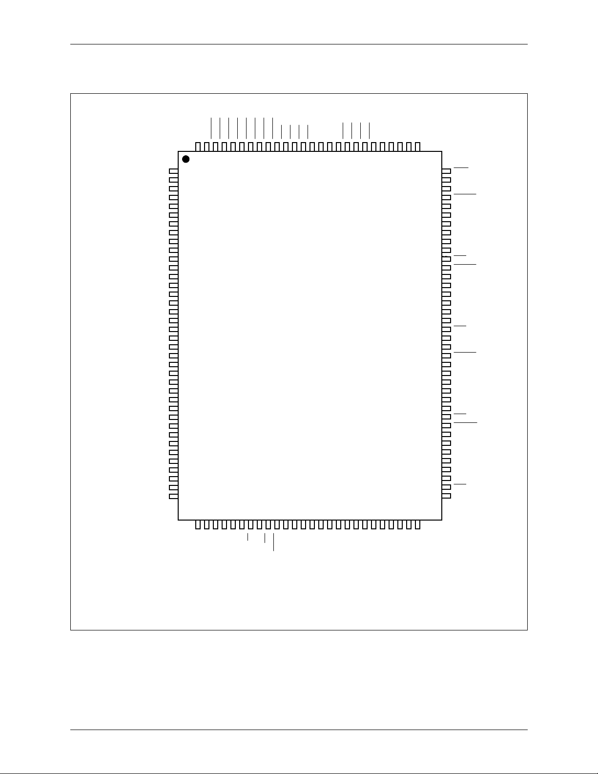
1
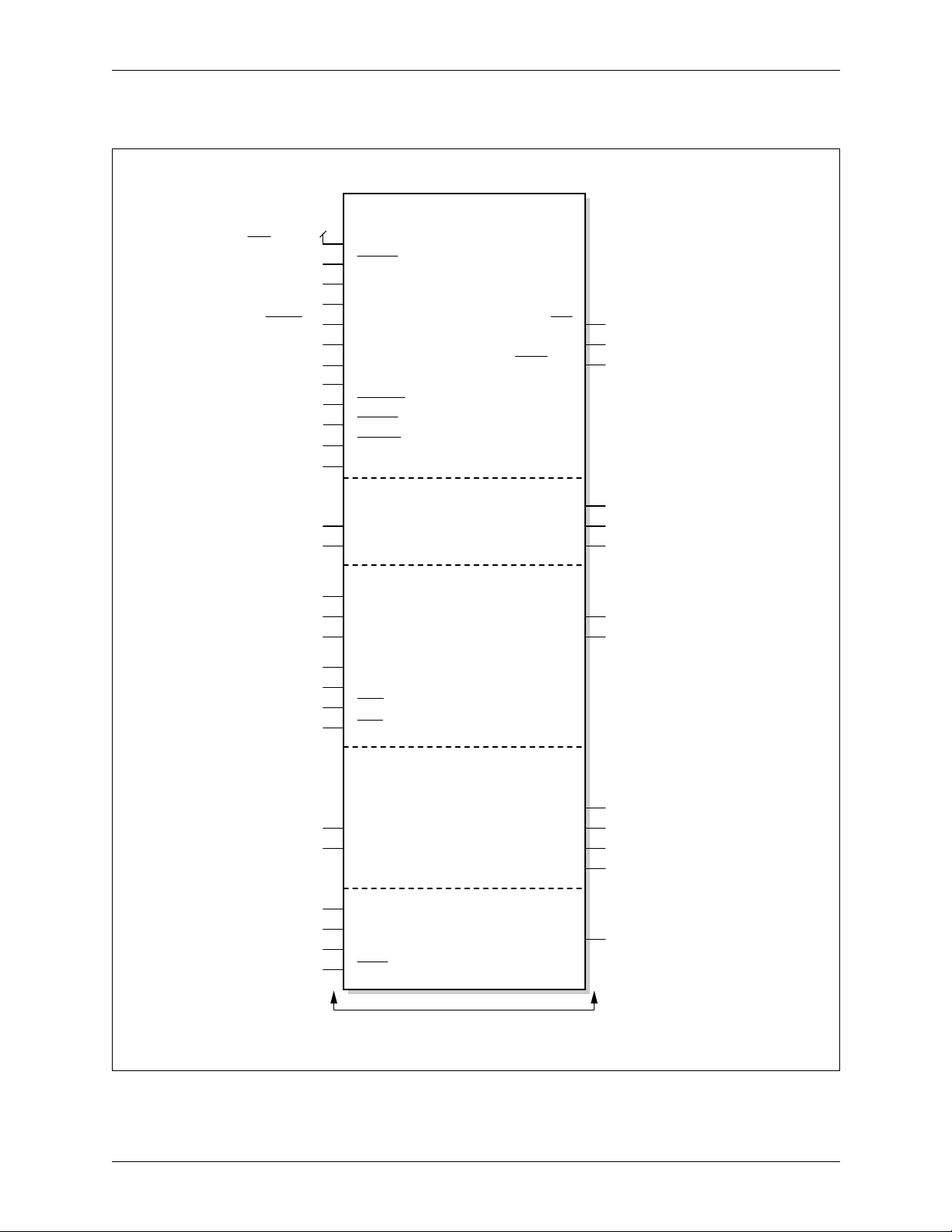
1.0 Pin Descriptions
The CN8380 is packaged in a 128-pin metric quad flat pack (MQFP). A pinout
diagram is illustrated in Figure 1-1. Logic diagrams are illustrated in Figure 1-2
and Figure 1-3. Pin labels and numbers, input/output functions, and descriptions
are provided in Table 1-1.
The following input pins contain an internal pull-up resistor (> 50 kΩ) and
may remain unconnected if unused or if the active high input state is desired:
XOE
[1:4]
TAIS
[1:4]
RAWMD
RLOOP
LLOOP
HM
UNIPOLAR
JDIR/SCLK
JSEL(2)/SDI
JSEL(1)/CS
JSEL(0)
RESET
HTERM
CLK_POL
PTS(2:0)
TDI (Unused if JTAG not connected)
TMS (Disables JTAG if not connected)
TCK (Unused if JTAG not connected)
TRST
[1:4]
[1:4]
[1:4]
(Unused if JTAG not connected)
N8380DSA Conexant 1-1
Advance Information
Page 14
1.0 Pin Descriptions CN8380
Figure 1-1. CN 8380 Pinout Diagram
CLADI
VAACL
GNDCL
REFCKI
VSS
VDD
CLK32
CLK1544
CLK2048
CLADO
VSS
RNEGO/BPV [4]
RPOSO/RDATO [4]
TPOSI/TDATI [4]
RNEGO/BPV [3]
RPOSO/RDATO [3]
TPOSI/TDATI [3]
RNEGO/BPV [2]
RPOSO/RDATO [2]
TPOSI/TDATI [2]
RNEGO/BPV [1]
RPOSO/RDATO [1]
TPOSI/TDATI [1]
VDD
RCKO [4]
TNEGI [4]
TCLK [4]
RCKO [3]
TNEGI [3]
TCLK [3]
VSS
VDD
RCKO [2]
TNEGI [2]
TCLK [2]
RCKO [1]
TNEGI [1]
TCLK [1]
1
2
3
4
5
6
7
8
9
10
11
12
13
14
15
16
17
18
19
20
21
22
23
24
25
26
27
28
29
30
31
32
33
34
35
36
37
38
EACKI
TACKI
128
127
RLOOP [2]
RLOOP [3]
RLOOP [4]
126
125
124
LLOOP [3]
LLOOP [4]
RLOOP [1]
123
122
121
TAIS [4]
LLOOP [1]
LLOOP [2]
120
119
118
128-Pin MQFP
TAIS [1]
TAIS [2]
TAIS [3]
117
116
115
CN8380
VSS
VDD
UNIPOLAR
114
113
112
RLOS [3]
RLOS [4]
111
110
RLOS [1]
RLOS [2]
109
108
VGG
107
Quad T1/E1 Line Interface
TDO
TDI
TMS
TCK
106
105
104
103
102
101
100
99
98
97
96
95
94
93
92
91
90
89
88
87
86
85
84
83
82
81
80
79
78
77
76
75
74
73
72
71
70
69
68
67
66
65
85
TRST
VAA
GND
RAWMD [4]
RRING [4]
RTIP [4]
VAAT [4]
GNDT [4]
XRING [4]
XTIP [4]
XOE [4]
RAWMD [3]
RRING [3]
RTIP [3]
VAAT [3]
GNDT [3]
XRING [3]
XTIP [3]
XOE [3]
GNDR
VAAR
RAWMD [2]
RRING [2]
RTIP [2]
VAAT [2]
GNDT [2]
XRING [2]
XTIP [2]
XOE [2]
RAWMD [1]
RRING [1]
RTIP [1]
VAAT [1]
GNDT [1]
XRING [1]
XTIP [1]
XOE [1]
HM
616263
N.C.
PTS(2)
PTS(1)
64
PTS(0)
LEGEND:
39404142434445464748495051
IRQ
RESET
HTERM
JATERR [4]
JATERR [3]
JATERR [2]
JSEL(0)
JDIR / SCLK
JSEL(1) / CS
JSEL(2) / SDI
JATERR [1] / SDO
CLK_POL
52
53545556575859
VSS
ZCS
N.C.
N.C.
VDD
N.C.
N.C.
N.C.
N.C.
60
N.C.
[#] - Port Number
(#) - Bit Number
8380_003
1-2 Conexant N8380DSA
Advance Information
Page 15
CN8380 1.0 Pin Descriptions
Quad T1/E1 Line Interface
Figure 1-2. CN83 80 Logic Diagram (Ho s t Mode)
Hardware/Host Mode
Hardware/Host Mode
Local Loopback
Local Loopback
Remote Loopback
Remote Loopback
Serial Data In
Serial Data In
Serial Clock In SCLK
Serial Chip Select
Transmit Positive Rail
Transmit Negative Rail
Serial Clock In SCLK
Serial Chip Select
Receive Tip
Receive Tip
Receive Ring
Receive Ring
Transmit Clock
Transmit Clock
Transmit Positive Rail
Transmit Negative Rail
PIO
I
I
I
I
I
I
I
I
PIO
I
I
I
I
I
I
I
I
I
I
I
I
HM
HM
RESETHardware Reset
RESETHardware Reset
LLOOP[1:4]
LLOOP[1:4]
RLOOP[1:4]
RLOOP[1:4]
SDI
SDI
CS
CS
RTIP[1:4]
RTIP[1:4]
RRING[1:4]
RRING[1:4]
TCLK[1:4]
TCLK[1:4]
TPOSI[1:4]
TPOSI[1:4]
TNEGI[1:4]
TNEGI[1:4]
Host Mode
Host Mode
Hardware
Control
Hardware
Interface
Control
Interface
Serial Port
Serial Port
Interface
Interface
(SERIO)
RLOS[1:4]
RLOS[1:4]
(SERIO)
Receiver
Receiver
(RCVR)
(RCVR)
Transmitter
Transmitter
(XMTR)
(XMTR)
RCKO[1:4]
RCKO[1:4] Receive Clock
RPOSO[1:4] Receive Positive Rail
RPOSO[1:4] Receive Positive Rail
RNEGO[1:4]
RNEGO[1:4]
XTIP[1:4]
XRING[1:4]
XRING[1:4] Transmit Ring
IRQ
IRQ
SDO
SD O Serial Data Out
XTIP[1:4] Transmit Tip
Interrupt Request
O
Interrupt Request
O
Receive Loss of Signal Status
O
Receive Loss of Signal Status
O
Serial Data Out
O
O
O
Receive Clock
O
O
O
Receive Negative Rail
O
Receive Negative Rail
O
Transmit Tip
O
O
Transmit Ring
O
O
1544 kHz All 1s Clock
1544 KHz All Ones Clock
2048 kHz All 1s Clock
2048 KHz All Ones Clock
Transmit Output Enable
Transmit Output Enable
Transmit All 1s
Transmit All Ones TAIS[1:4]
CLAD Input CLK32 32.768 MHz Clock Out
CLAD Input CLK32 32.768 MHz Clock Out
Test Mode Select
Test Mode Select
Test Data In
Test Data In
Test Reset In
Test Reset In
8380_004
I
I
I
I
I
I
I
I
I
I
TACKI
I
EACKI
I
XOE[1:4]
I
TAIS[1:4]
I
CLADI
I
I
REFCKIReference Clock
I
TCKTest Clock In
I
TMS
I
TDI
I
TRST
TACKI
EACKI
XOE[1:4]
Clock Rate
Clock Rate
Adapter (CLAD)
Adapter (CLAD)
CLADI
REFCKIReference Clock
Boundary Scan
TCKTest Clock In
TMS
TDI
TRST
PIO = Programmable I/O
Boundary Scan
(JTAG)
(JTAG)
I = Input, O = Output
I = Input, O = Output
PIO = Programmable I/O
O
O
CLK1544
CLK1544
CLK2048 E1 Line Rate Clock Out
CLK2048 E1 Line Rate Clock Out
CLADO
CLADO
TDO
TDO
T1 Line Rate Clock Out
O
T1 Line Rate Clock Out
O
O
O
CLAD Output
O
O
CLAD Output
Test Data Out
O
Test Data Out
O
N8380DSA Conexant 1-3
Advance Information
Page 16
1.0 Pin Descriptions CN8380
Figure 1-3. CN83 80 Logic Diagram (Ha rdware Mode)
Hardware Mode
VDD
I
I
I
I
I
I
I
I
I
I
I
I
I
HM
RESETHardware Reset
JDIR
JSEL(2:0)
UNIPOLAR
HTERM
PTS(2:0)
CLK_POL
RAWMD[1:4]Raw Mode Select
LLOOP[1:4]
RLOOP[1:4]
ZCS
RTIP[1:4]
RRING[1:4]
Hardware/Host Mode
Jitter Attenuator Path
Jitter Attenuator Size
Unipolar/Bipolar
Transmitter Termination
Clock Polarity
Local Loopback
Remote Loopback
Zero Code Suppression
Receive Tip
Receive Ring
Hardware
Control
Interface
Receiver
(RCVR)
Quad T1/E1 Line Interface
IRQ
JATERR[1:4]
RLOS[1:4]
RCKO[1:4]
RPOSO[1:4] Receive Positive Rail
RNEGO[1:4]
O
Interrupt Request
O
Jitter Attenuator Error Status
Receive Loss of Signal StatusTransmit Pulse Template
O
O
Receive Clock
O
Receive Negative Rail
O
Transmit Clock
Transmit Positive Rail
Transmit Negative Rail
1544 kHz All 1s Clock
2048 kHz All 1s Clock
Transmit Output Enable
Transmit All 1s
CLAD Input
Test Clock In
Test Mode Select
Test Data In
Test Reset In
I
I
I
I
I
I
I
I
I
I
I
I
I
TCLK[1:4]
TPOSI[1:4]
TNEGI[1:4]
TACKI
EACKI
XOE[1:4]
TAIS[1:4]
CLADI
REFCKIReference Clock
TCK
TMS
TDI
TRST
PIO = Programmable I/O
Transmitter
(XMTR)
XRING[1:4]
Clock Rate
Adapter (CLAD)
Boundary Scan
(JTAG)
I = Input, O = Output
XTIP[1:4]
CLK32
CLK1544
CLK2048 E1 Line Rate Clock Out
CLADO
TDO
O
Transmit Tip
O
Transmit Ring
O
32.768 MHz Clock Out
O
T1 Line Rate Clock Out
O
8 KHz Clock Out
O
O
Test Data Out
8380_005
1-4 Conexant N8380DSA
Advance Information
Page 17

CN8380 1.0 Pin Descriptions
Quad T1/E1 Line Interface
Table 1-1. Ha rdware Signal Definitions (1 of 5)
Pin Label Signal Name I/O Definition
Receiver
RPOSO[1:4]
RDATO[1:4]
RNEGO[1:4]
BPV[1:4]
RCKO[1:4] RX Clock Output O Receive clock output . RCKO is the RPLL recovered l ine rate clock or jitter
RX Positive Rail
(Bipolar Mode)
RX Data (Unipolar
Mode)
RX Negative Rail
(Bipolar Mode)
Bipolar Violation
(Unipolar Mode)
O Line rate data ou tput on the r isi ng or fa lling edg e of RCK O. Th e cloc k edge
is determined by the CLK_POL pin in Hardware Mode or the CLK_POL
register bit [RLIU_CR; addr n1] in Host Mode. In bipolar mode, a high
signal indicates receipt of a positive AMI pulse on RTIP/RRING inputs. In
unipolar mode, RPOSO is redefi ned as RDATO and a high signal indica tes
either a positive or negative AMI pulse on RTIP/RRING inputs.
RPOSO/RDATO is three-stated during device reset.
O Line rate data output on rising or falling edg e of RCKO. The clock e dge is
determined by the CLK_POL pin in Hardware Mode or the CLK_POL
register bit [RLIU_CR; addr n1] in Host Mode. In bipolar mode, a high
signal indicates receipt of a negativ e AMI pul se on RTIP/RRING inputs. In
unipolar mode , RNEG O is rede fined as BP V, and a high si gnal in dicate s the
reception of a BPV which is not part o f a ZCS code (B8ZS or H DB3).
RNEGO/BPV is three-stated during device reset.
attenuated clock output, based on the programmed jitter attenuator
selection. RCKO is three-stated during devic e reset.
RTIP[1:4]
RRING[1:4]
Receive Tip
Receive Ring
I Differential AMI data inputs for direct connection to receive transformer.
Transmitter
TPOSI[1:4]
TDATI[1:4]
TNEGI[1:4] Tx Negative Rail
TCLK[1:4] TX Clock Input I/O Transmit line rate clock. TCLK is the transmit clock for TPOSI and TNEG I
TACKI
EACKI
[1:4] Transmit Output
XOE
[1:4] Transmit AIS
TAIS
Tx Positive Rail
(Bipolar Mode)
Tx Data (Unipolar
Mode)
Input
T1 AIS Clock
E1 AIS Clock
Enable
Alarm
I Positive rail, line rate data source for transmitted XTIP/XRING output
pulses. Data is sampled on the falling edge of TCLK. In bipolar mode, a
high on TPOSI causes a positive output pulse on XTIP/XRING; and a high
on TNEGI causes a negative output pulse. In unipolar mode, TPOSI is
redefined as TDATI and accepts single-rail NRZ data. TNEGI is not used in
unipolar mode.
I Negative rail, l ine rate data input on TCLK falling edge. Refe r to TPOSI
signal definition.
data inputs and for transmitter timing. Normally, TCLK is an input and
samples TPOSI/TNEGI on the falling edge. In Host Mode, TCLK can be
configured as an output to supply a line rate transmit clock from the
CLAD. The timing reference for the TCLK output (and CLAD) can be
selected from six sources.
I
Alternate T1 and E1 transmit clock used to transm it AIS (all 1s alarm
signal) when the primary transmit clock source, TCLK, fails. TACKI (T1) or
EACKI (E1) is either manually or automatically swi tched to replace TCLK
I
[LIU_CTL; addr n3]. Syste ms without an AIS clock should connect TACKI
and EACKI to gro und.
P
A low signal enables XTIP and XRING output drivers. Otherwise outputs
I
are high impedance.
P
In Hardware Mode, a low signal causes AIS (unframed all 1s)
I
transmission on XTIP/XRING outputs. In Host Mode, these pins can be
enabled or disabled [LIU_CTL; addr n3]. If disabled, they are not used and
may be left unconnected.
N8380DSA Conexant 1-5
Advance Information
Page 18

1.0 Pin Descriptions CN8380
Quad T1/E1 Line Interface
Table 1-1. Ha rdware Signal Definitions (2 of 5)
Pin Label Signal Name I/O Definition
XTIP[1:4]
XRING[1:4]
Transmit Tip
Transmit Ring
O Complementary AMI transmitter line outputs for direct connection to
transmit transformer. Optionally, both outputs are three-stated when XOE
is high.
Clock Rate Adapter (CLAD)
CLADI CLAD Input I CLAD input timing reference used to phase/frequency lock the CLAD
outputs to an input clock frequency selected in the range of 8 kHz to
32,768 kHz [CLAD_CR; addr 02]. Systems which do not use CLADI should
connect CLADI to ground. In Hardware Mode, the CLAD timing reference
automatically switches to internal free-run operation if clock edges are not
detected on CLADI pin.
REFCKI Reference Clock I System must apply a 10 MHz ± 50 ppm (E1) or +
to act as the frequency reference for the internal numericall y controlled
oscillator (NCO). REFCKI det ermines the frequency accuracy and stability
of the CLAD output clocks when operating in free-run mode [CLAD_CR;
addr 02]. REFCKI is the baseband reference for all CLAD/JAT functions
and is used internall y to generate clocks of various frequency locked to a
selected receive or external clock.
32 ppm (T1) clock signal
Note
: REFCKI is always required.
CLK32 32 MHz Clock
Output
CLK1544 T1 Clock Output O Fixed rate 1.544 MHz T1 line rate clock output provided by the CLAD. May
CLK2048 E1 Clock Output O Fixed rate 2.048 MHz E1 line rate clock output provided by the CLAD. May
CLADO CLAD Output O In Hardware Mode, CLADO is a fixed rate 8 kHz clock output pro v ided by
O Fixed rate 32.768 MHz cl ock output provided by t he CLAD. May be used
by framers, such as the CN8398 octal T1/E1 framer, to provide system
timing reference.
be used for TCLK or TACKI clock sources. This clock is locked to the
selected CLAD timing ref e rence.
be used for TCLK or EACKI clock sources. This clock is locked to the
selected CLAD timing ref e rence.
the CLAD. In Host Mode, CLADO may be configured to operate at one of
14 different clock freq uencies [CSEL; addr 03] that include T1 or E1 line
rates. CLADO is typically programmed to supply system clocks that are
phase-locked to the selected receive or CLAD timing reference [CLAD_CR;
addr 02].
Hardware Control Signals
HM Hardware Mode
P
A high on HM places the device in Hardware Mode, enabling all hardware
I
control pin functions. A low on HM places the device in H ost Mode,
disabling some hardware-mode-only pin functions and enabling the serial
port signals on the dual function pins listed bel ow. The serial po rt signals
allow serial host access to the device registers. Refer to the Host Serial
Control Signals se ction of this table.
JSEL(2) / SDI
[1:4] Raw Mode
RAWMD
JSEL(1) / CS
JDIR / SCLK JATERR(1) / SDO
P
Low selects receiver Raw mode. Applicable only in Hardware Mode. In
I
Raw mode, RPOSO and RNEGO represent the data slicer outputs and
RCKO is the logical OR of RPOSO and RNEGO.
1-6 Conexant N8380DSA
Advance Information
Page 19

CN8380 1.0 Pin Descriptions
Quad T1/E1 Line Interface
Table 1-1. Ha rdware Signal Definitions (3 of 5)
Pin Label Signal Name I/O Definition
RESET Hardware Reset
P
Active low asynchronous hardware reset. A falling edge forces registers to
I
their default, power-up state. Output pins are forced to the high impedance
state while RESET is ass erted. RESET is not mandat ory at power-up
because an internal power-on reset circuit performs an identic al function.
P
UNIPOLAR Unipolar Mode
Select
Applicable only in Hardware Mode. A high signal on UNIPOLAR configures
I
all RPOSO outputs and TPOSI inputs to operate with unipolar, NRZformatted data. In this mo de, RN EGO report s non-ZC S BPVs and TNE GI is
not used. A low signal on UNIPOLAR configures all channels’
RPOSO/RNEGO and TPOSI/TNEGI interfaces to operate with bipolar,
dual-rail, NRZ formatted data .
P
ZCS Zero Code
Suppression
Select
Applicable only in Hardware Mode. A high signal on ZCS enables the
I
transmit ZCS encoder and the receive ZCS decoder if unipolar mode is
enabled (UNIPOLAR = 1). In Bipolar Mode (UNIPOLAR = 0), the ZCS
encoder and decoder are disabled and ZCS is ignored.
P
CLK_POL Rx Clock Polarity
Select
Applicable only in Hardware Mode. High s ets RPOSO/R NEGO to be output
I
on the falling ed ge o f RC KO. Low sets RPOSO/RN EGO to be o utp ut on the
rising edge of RCKO
PTS(2:0) Transmit Pulse
T emplate Select
P
Applicable only in Hardware Mode. The PTS(2:0) control bus selects the
I
transmit pulse template and the line rate (T1 or E1) globally for all
channels. Refer to the description of HTERM in this table and to the
transmit pulse configurations in Table 2-3.
P
HTERM Transmitter
Hardware
Termination
Applicable only in Hardware Mode. If an external tran smit termination
I
resistor is used to meet return loss specifications; a transformer with a 1:2
turns ratio is used, and HTERM i s set high to allow the transmitter to
compensate for the increased load. Refer to the Transmitter section of this
table and Tables 2-4 through 2-8 for transmitter termina ti on con fig ura ti on
options.
IRQ
Interrupt Request
D
Active low, open drain output. In Host Mode, IRQ indicates one or more
O
pending interrupt requests ([ISR; addr n6] and [CSTAT; addr 06]). In
Hardware Mode, IRQ is the logical NOR of the four internal transmitter
driver performance monitor outputs.
P
JSEL(2:0) Jitter Attenuator
Select
Applicable only in Hardware Mode. The JSEL and JDIR pins determine the
I
JAT configuration. JSEL(2:0) enables and selects the JAT depth as shown
in the table below. SDI/JSEL(2) and CS /JSEL(1) are dual function pins.
JSEL(2:0) JAT Mode
000 8 bits
001 16 bits
010 32 bits
011 64 bits
100 128 bits
111 Disable JAT
P
JDIR Jitter Attenuator
Direction
Applicable only in Hardware Mode. JDIR determines the path in which the
I
JAT is inserted. If JDIR is low, the JAT (if enabled) is placed in the receive
path; if high, the JAT (if enabled) is placed in the transmit path. Refer to
the description for JSEL(2:0). SCLK/JDIR is a dual function pin.
JATERR[1:4] Jitter Attenuator
Error
O Applicable only in Hardware Mode. A high on JATERR indicates an
overflow or underflow error in the jitter attenuator elastic store.
JATERR(1) / SDO is a dual function pin.
N8380DSA Conexant 1-7
Advance Information
Page 20
1.0 Pin Descriptions CN8380
Quad T1/E1 Line Interface
Table 1-1. Ha rdware Signal Definitions (4 of 5)
Pin Label Signal Name I/O Definition
RLOS [1:4] Receive Loss of
Signal
ORLOS is asserted low when 100 (T1) or 32 (E1) consecutive 0s (no
pulses) are received at the l ine interface or when the received signal level
is approximately 1 8 dB below nominal for at least 1 ms.
LLOOP [1:4]
Local Loop
P
These pins are always enabled in Hardware Mode and may be en abled or
I
disabled in Host Mode [LIU_CTL; addr n3]. A low on LLOOP initiates Local
RLOOP [1:4]
Remote Loop
Analog Loopback and a low on RLOOP initiates Remote Line Loopback.
P
I
Local Digital Loo pback is initiated if both signals are asserted together.
Boundary Scan Signal s (JTAG)
TDO Test Data Output O Test data output p e r IEEE Std. 1149 .1-1990. Three-st ate output used for
reading all serial conf iguration and test data f r om internal test logic.
Updated on the falling edge of TCK.
P
TDI Test Data Input
Test data input per IEEE Std. 1149.1-1990. Used for loading all serial
I
instructions and data into internal test logic. Sampled on the rising edge of
TCK. TDI may be left unconnected if not us ed.
TMS Test Mode Select
P
Active-low test mode select input per IEEE Std 1149.1-1990. Internally
I
pulled-up input signal use d t o co ntrol the test lo gi c state machine.
Sampled on the risi ng edge of TCK. TMS may be left unconnected if not
used.
P
TCK Test Clock
Test clock input per IEEE Std. 1149.1-1990. Used for all test interface and
I
internal test-logic operations. If not used, TCK should be pulled low.
TRST
Reset
P
Active low reset. TRST is pulled up internally and may be left unconnected
I
if not used.
Host Serial Control Signals
CS Chip Select
SDI Serial Data In
P
In Host Mode, CS is an active low input used to enable read/write access
I
with the host serial control port. CS
P
In Host Mode, SDI is the serial data input for the host serial control port.
I
/JSEL(1) is a dual function pin.
SDI/JSEL(2) is a dual function pin.
SDO Serial Data Out O In Host Mode, SDO is the serial data output for the host seria l control por t.
SDO/JATERR[1] is a dual function pin.
SCLK Serial Clock
P
In Host Mode, SCLK is the serial clock input for the host serial control
I
port. SCLK/JDIR is a dual function pin.
Power Supply Pins and No-Connect Pins
VAA
GND
VAAT[1:4]
Analog Supp ly
Ground
Tx Driver Supply
I+3.3 V + 5%. Power supply pair for the analog circuitry.
I+3.3 V +
5%. Power supply pairs for the transmitter driver circuitry. These
pin pairs should each be bypassed with a tantalum capacitor value of at
GNDT[1:4]
VAAR
GNDR
Ground
Rx Analog Supp ly
Ground
least 10
I + 3.3 V +
µF.
5%. Power supply pair for the analog receiver circuitry.
1-8 Conexant N8380DSA
Advance Information
Page 21

CN8380 1.0 Pin Descriptions
Quad T1/E1 Line Interface
Table 1-1. Ha rdware Signal Definitions
(5 of 5)
Pin Label Signal Name I/O Definition
VAACL
GNDCL
VDD
VSS
VGG ESD Rail I To insure 5 V tolerance in mixed + 5 V / + 3.3 V systems, this input must
N.C. No Connect — No-connect pins are reserved for future device compati bility and should
NOTE(S):
1. I/O Types:
I = Standard input
P =
Input with internal pull-up resister
I
O = Standard output
OD = Output with open drain
2. Legend:
[#] = Port number
(#) = Bit number
CLAD Supply
Ground
Digital Supply
Ground
I + 3.3 V + 5%. Power supp ly pair for the CLAD PLL circuitry.
I + 3 .3 V + 5%. Power supply pairs for the di gital circuitry.
be connected to + 5 V. If all logic input signals are 3.3 V levels, then this
pin may be connected to the 3.3 V supply.
be left unconnected.
N8380DSA Conexant 1-9
Advance Information
Page 22

1.0 Pin Descriptions CN8380
Quad T1/E1 Line Interface
1-10 Conexant N8380DSA
Advance Information
Page 23

2
2.0 Circuit Description
2.1 Overview
The CN8380 includes four identical T1/E1 transceiver channels and a common
CLAD packaged in a 128-pin MQFP carrier. It is designed to interface T1/E1
framers, or to operate as a stand-alone line interface for synchronous or
plesiochronous mappers and multiplexers. The CN8380 is ideal for high line
density, short-haul applications that require low power (3.3 V supply) operation.
The configurable T1/E1 operation and common line interface design allow s
support for single-board T1 and E1 designs.
Customer premise applications are supported by an on-chip JAT which
conforms to AT&T PUB 62411 and a selectable transmit pulse shape which
conforms to FCC Part 68, Pulse Option A. Selectable unipolar or bipolar interface
options and internal ZCS encoding and decoding are useful in many multiplexer
and mapper applications.
In the most simple configuration, Hardware Mode, the device is controlled
using dedicated hardware control pins. In this mode, the four channels are
configured globally to identical operating modes (T1, E1, transmit termination,
jitter attenuators, and so on). Each channel has device pins dedicated for channel
control and status, such as loopback controls, bipolar/unipolar interface modes,
and loss of signal indicators. Hardware Mode is selected by pulling the HM pin
high.
Host Mode allows control of the device through a 4-line serial port. In this
mode, all control and status functions can be accessed using internal registers.
Several additional features are also available in Host Mode, such as individual
channel operating mode configuration (T1 /E1, transmit termination, jitter
attenuators, etc.) and programmable CLAD output frequencies. Host Mode is
selected by grounding the HM pin.
The CN8380 incorporates printed c irc uit board testability circuits in
compliance with IEEE Std P1149.1a–1993, IEEE Standard Test Access Port and
Boundary–Scan Architecture, commonly known as JTAG (Joint Test Action
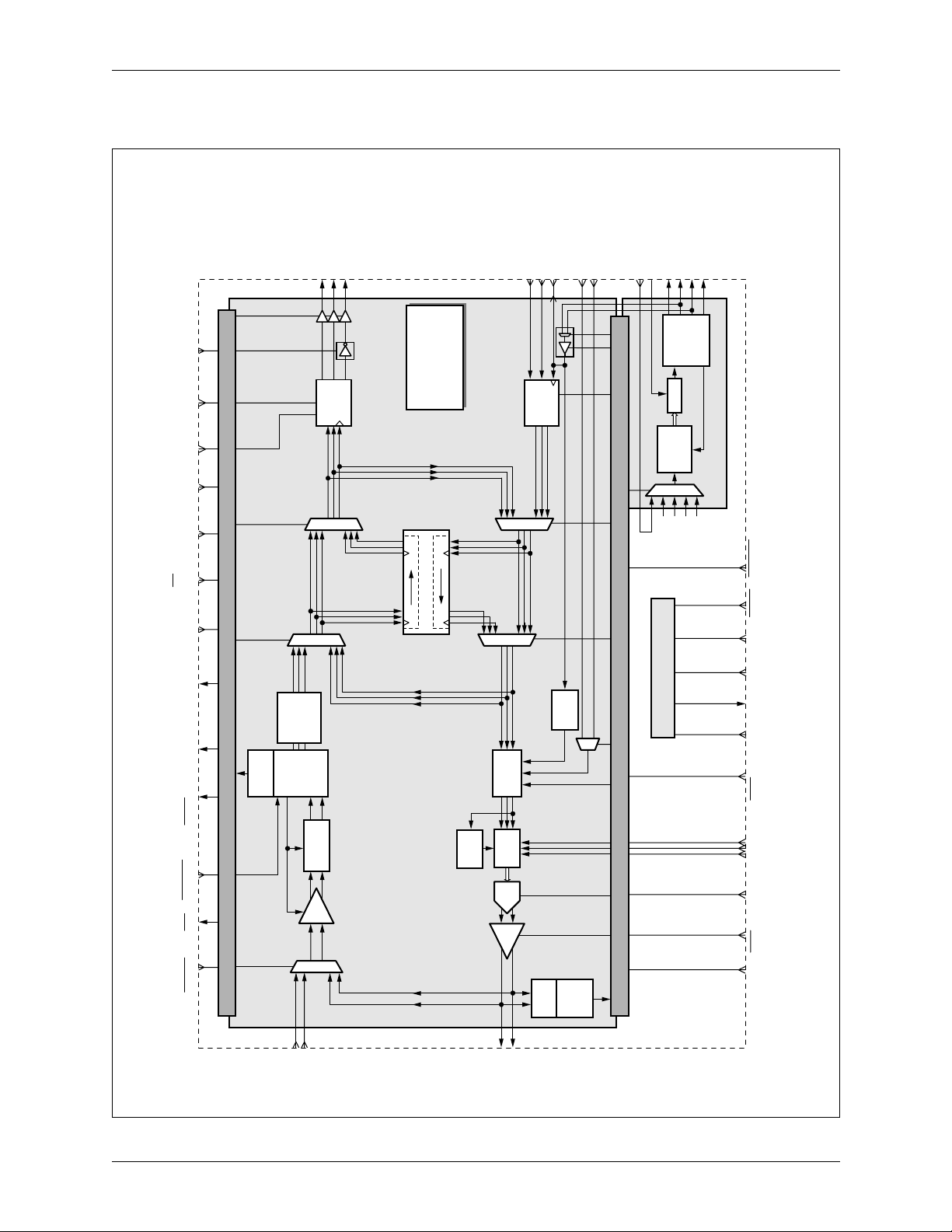
Group). A detailed block diagram is displayed in Figure 2-1.
N8380DSA Conexant 2-1
Advance Information
Page 24
2.0 Circuit Description CN8380
2.1 Overview
Figure 2-1. Detailed Block Diagram
CLK_POL
UNIPOLAR
ZCS
JDIRLLOOP[n] IRQ JATERR[n]
SCLK
RPOSO[n]
RNEGO[n]
RCKO[n]
RZCS
Decode
0
1
Note:
Only one LUI is
shown. The other
three are identical.
Remote
Line
Loopback
1
TCLK[n]
TPOSI[n]
TNEGI[n]
TZCS
Encode
0
TACKI
EACKI
Quad T1/E1 Line Interface
CLADI
CLK1544 (1.544 MHz)
REFCKI
CLADO
CLK32 (32.768 MHz)
CLK2048 (2.048 MHz)
Chain
Divider
NCO
CLAD
Phase
Detector
CS
JSEL(1) JSEL(0)RLOS[n]
SDI
JSEL(2)
SDO
JATERR[1]
RAWMD[n]
Control
RLOS
Detect
1
Clock
Recovery
Peak
Detect
0
RPLL
and
Slicer
Adaptive
Equalizer
VGA
1
RCKO[3]
RCKO[2]
RCKO[1]
RCKO[4]
Jitter Attenuator
0
Local
Digital
Loopback
Local
Analog
Loopback
8X
TPLL
1
AIS
Gen
Pulse
Shape
DAC
DRV
0
Control
JTAG
Mon
Clock
CKT
DPM
Short
Detect
TRSTTCLKTDO
TDI TMS RLOOP[n]HM
PTS(2:0)
HTERM
XOE[n] TAIS[n]
RTIP[n]
RRING[n]
XTIP[n]
XRING[n]
8380_006
2-2 Conexant N8380DSA
Advance Information
Page 25

CN8380 2.0 Circuit Description
Quad T1/E1 Line Interface
2.2.1 Hardware Mode
2.2.2 Host Mode
2.2 Configuration and Control
2.2 Configuration and Control
In Hardware Mode, the device is controlled using dedicated hardware control
pins. In this mode, the four channels are configured globally to identical
operating modes (T1, E1, tr ansmit termination, j itter atten uators, and so o n). Each
channel has device pins dedicated for channel control and status, such as
loopback controls, bipolar /unipolar i nterface modes, and loss of sig nal indicators.
Refer to Table 1-1,
pins. Hardware Mode is selected by pulling the HM pin high.
In Host Mode, control of the device is through a four-line serial port. In this
mode, all control and status functions can be accessed using internal registers.
Refer to Chapter 3.0,
selected by grounding the HM pin.
Hardw are Signal Definitions
Registers
, for a description of each register. Host Mode is
, for a description of all hardw are
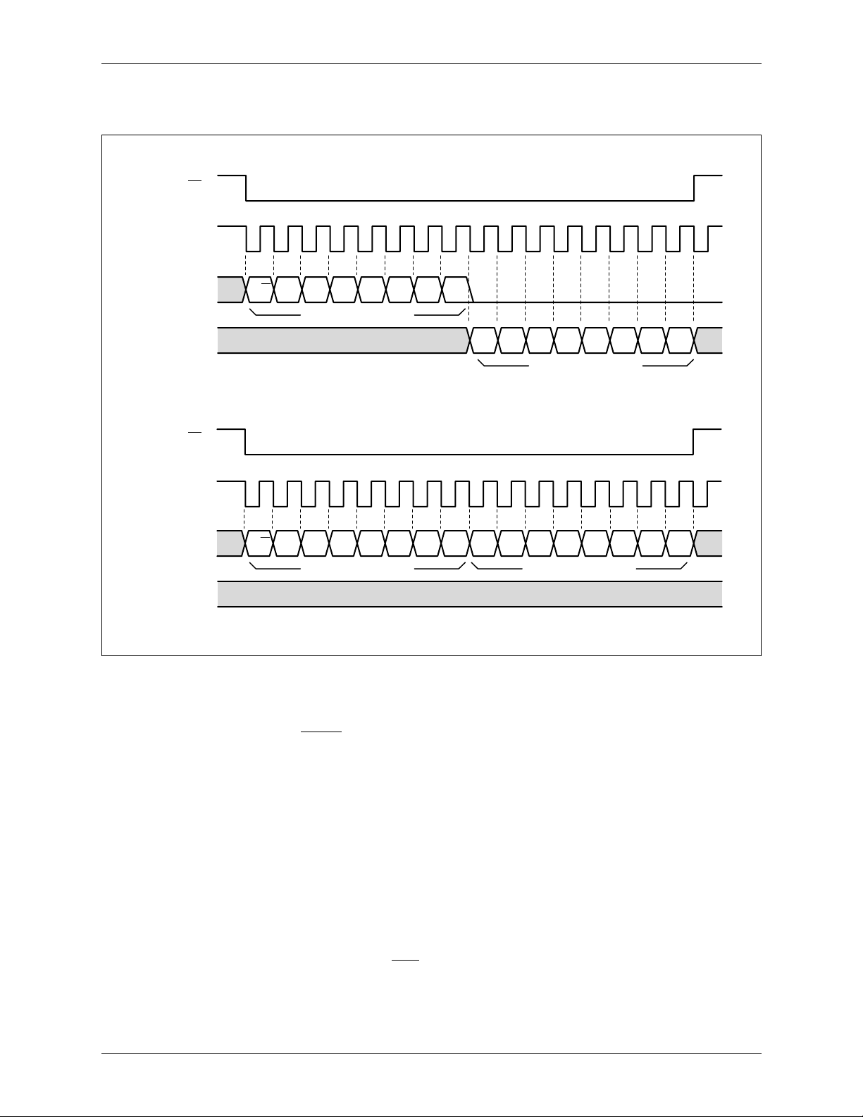
2.2.3 Host Serial Control Interface
The CN8380 serial interface is a four-wire, slave interface which allows a host
processor or framer with a compatible master serial port to communic ate with t he
LIU. This interface allows the host to control and query the CN8380 status by
writing and reading internal registers. One 8-bit register in the LIU can be written
via the SDI pin or read from the SDO pin at the clock rate determined by SCLK.
The serial port is enabled by pulling the chip select pin,
the read and write cycles. Refer to Figure 2-2 for host serial port signals.
The serial interface uses a 16-bit process for each write or read operation.
During a write or read operation, an 8-bit cont rol word, consistin g of a read /wri te
control bit (R/W) and a 7-bit LIU register address (A[6:0]) is transmitted to the
LIU using the SDI pi n. If the operation is a write operation (R/W = 0), an 8-bit
register data (D[7:0]) byte follows the address on the SDI p in. This data is
received by the CN8380 and stored in the addressed register. If the operation is a
read operation (R/W = 1), the CN83 80 output s th e addr essed register contents on
the SDO pin. The signal input on SDI is sampled on the SCLK falling edge, and
data output on SDO changes on the SCLK rising edge.
CS
, active (low) during
N8380DSA Conexant 2-3
Advance Information
Page 26
2.0 Circuit Description CN8380
2.2 Configuration and Control
Figure 2-2. Host Serial Port Signals
CS
SCLK
R/W
SDI
SDO
CS
A0 A1 A2 A3 A4 A5 A6
Quad T1/E1 Line Interface
Read Timing
Address/Control Byte
D0 D1 D2 D3 D4 D5 D6 D7
Register Data Byte
Write Timing
SCLK
SDI
SDO
8380_007
2.2.4 Reset
A0 A1 A2 A3 A4 A5 A6
R/W
Address/Control Byte
D0 D1 D2 D3 D4 D5 D6 D7
Register Data Byte
The CN8380 supports three reset methods: power-on reset, hard reset i ni tiat ed by
RESET
the
pin, and soft reset initiated by the RESET bit in the Global
Configuration Register [GCR; addr 01]. In Host Mode, all three reset methods
produce the same results as listed below. In Hardware Mode, power-on reset and
hard reset produce the same results as shown; and soft reset is not applicable.
After RESET is complete, t he following is true:
Hardware Mode Host Mode
Digital receiver outputs
(RPOSO[1:4] and RNEGO[1:4],
RCKO[1:4]) are enabled.
Digital receiver outputs (RPOSO[1:4]
and RNEGO[1:4], RCKO[1:4]) are
three-stated.
Transmitter line outputs (XTIP[1:4]
and XRING[1:4]) are enabled
XOE
(controlled by
).
Transmitter line outputs (XTIP[1:4]
and XRING[1:4]) are three-stated.
2-4 Conexant N8380DSA
Advance Information
Page 27

CN8380 2.0 Circuit Description
Quad T1/E1 Line Interface
2.2.4.1 Power-on Reset
2.2 Configuration and Control
Hardware Mode Host Mode
CLK1544, CLK2048, and CLADO
clock outputs are enabled.
Transmitter clocks, TCLK[1:4], are
configured as inputs.
IRQ
The
pin is enabled (controlled
CLK1544, CLK2048, and CLADO
clock outputs are three-stated.
Transmitter clocks, TCLK[1:4], are
configured as inputs.
IRQ
The
pin is three-stated.
by DPM).
All interrupt sources are disabled.
All configuration registers are set to
default values as listed in Section 3.1,
Address Map
.
An internal power-on reset process is initiated during power-up. When VDD has
reached approximately 2.6 V, the internal reset process begins and continues for
300 ms maximum if REFCLK is applied. If REFCLK is not pr esen t, t he CN83 80
remains in the reset state.
2.2.4.2 Hard Reset
2.2.4.3 Soft Reset
Hard reset is initiated by bringing the
internal reset process completes in 5 µs maximum. If the
continuously, the clock and dat a o utp ut s and th e
following output pins are forced to high impedance while
RESET
pin active (low). Once initiated, the
RESET
pin is held active
IRQ
pin remain three-stated . The
RESET
is held active:
RPOSO[1:4] CLADO
RNEGO[1:4] TCLK[1:4]
RCKO[1:4]
XTIP[1:4]
IRQ
RLOS[1:4]
XRING[1:4:] JATERR[1:4]
CLK1544 SDO
CLK2048 TDO
In Host Mode, soft reset is in itiated by writing a one to the RESET bit in the
Global Configuration register [addr 01]. The RESET bit is self-clearing. Once
initiated, the internal reset process comp letes in 5 µs maximum and the device
enters normal operation.
N8380DSA Conexant 2-5
Advance Information
Page 28
2.0 Circuit Description CN8380
2.3 Receiver
Quad T1/E1 Line Interface
2.3 Receiver
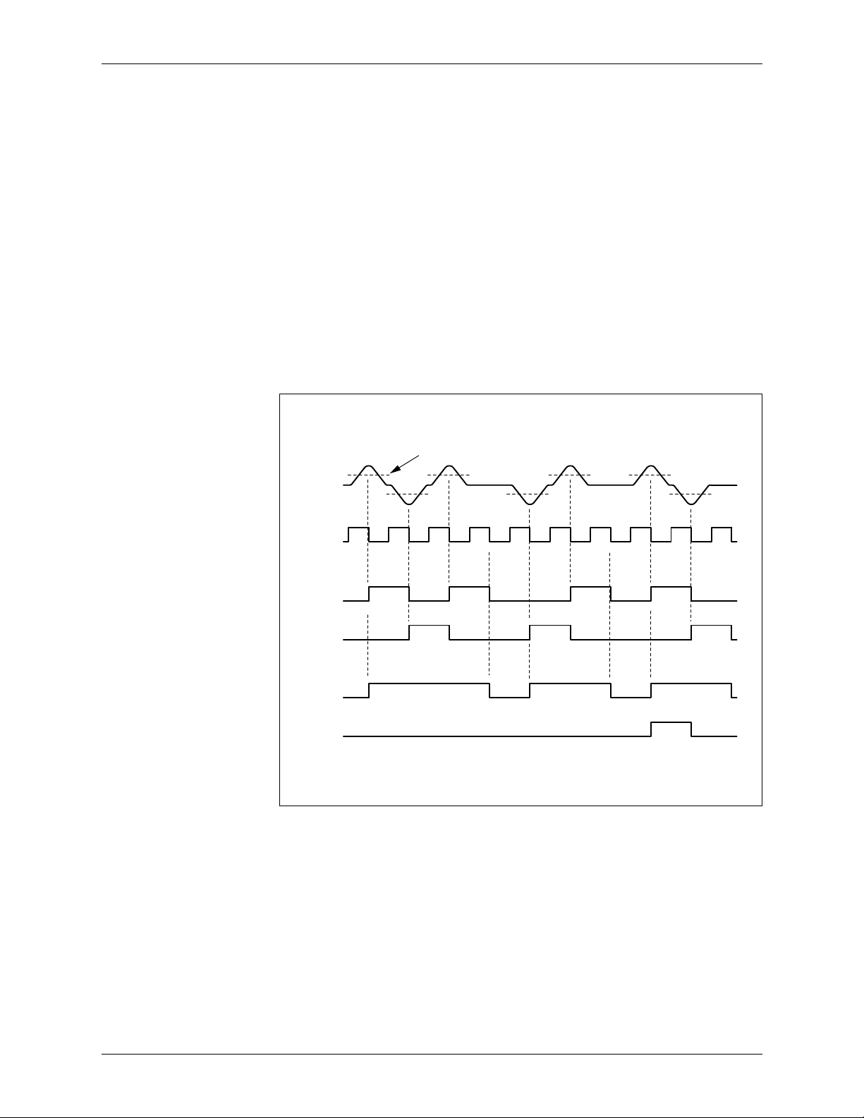
Bipolar AMI pulses are input on the receiver input pins, RTIP[n] and RRING[n].
The receiver recovers clock and data from the AMI signal which has been
attenuated and distorted due to the line characteristics. The AMI pulses are
converted into bipolar or unipolar, NRZ data and output on RPOSO[n] and
RNEGO[n], along with the recovered clock on RCKO[n]. Figure 2-3 illustrates
the relationship between the AMI received signal, the recovered clock, and the
data outputs. This section discusse s each receiver block from the line input to the
digital outputs.
Figure 2-3. Receiver Signals
Data Slicer Level
(50% of Peak)
Internal
Equalized
Received
Signal
2.3.1 Data Recovery
RCKO
RPOSO
(Bipolar)
RNEGO
(Bipolar)
RDATO
(Unipolar)
BPV
(Unipolar)
111 11 1100
BPV
The receiver recovers data by normalizing th e input signal wit h an aut omatic ga in
control (AGC) circuit, removing distortion with an equalizer, and extracting the
data using a data slicer . The transfer functio n of the equalizer is adjusted based on
the average peak value of the input signal. The AGC maintains the equalizer’s
average peak output level to a constant value. The data slicer compares the
equalizer output to a threshold value equal to 50% of the average peak equalizer
output level and produces both positive and negative pulse detect signals. The
data slicer outputs are re-t imed using the recovered clock and routed to the RZCS
decoder (or to the JAT ).
8380_008
2-6 Conexant N8380DSA
Advance Information
Page 29

CN8380 2.0 Circuit Description
Quad T1/E1 Line Interface
2.3.1.1 Raw Receive Mode
Optionally, the data slicer outputs, before re-timing, can be routed directly to the
RPOSO and RNEGO digital output pins. This option (raw receive mode) is
selected by asserting the
RAWMD register bit [RLIU_CR; addr n1] in Host Mode. In raw receive mode,
RCKO is replaced by the logical OR of the RPOSO and RNEGO output signals.
This mode is useful in applications which provide external clock and data
recovery. Figure 2-4 illustrates the raw mode receiver signals.
Figure 2-4. Raw Mode Receiver Signals
Internal
Equalized
Received
Signal
RPOSO
(RAW Mode)
RNEGO
(RAW Mode)
Data Slicer Level
(50% of Peak)
RAWMD
2.3 Receiver
[n] pin in Hardware Mode or by asserting the
BPV
RCKO
(RAW Mode)
8380_009
2.3.1.2 Sensitiv ity
2.3.1.3 Bridge Mode
The receiv er is capab le of recovering signals with cab le attenu ation in the range of
+3 to –12 dB in E1 and T1 modes. The receiver is configured by setting register
bits appropr iately in Host Mode or by setting configuration pins in Hardware
Mode. See Table 2-1for line compatible modes.
Table 2-1. Line Compatible Modes
Mode Receiver Sensitivity
T1 +3 dB to –12 dB –18 dB –18 dB 100 zeros
T1/E1 20 dB
Bridge
E1 +3 dB to –12 dB –18 dB –18 dB 32 zeros
–17 dB to –26 dB NA NA 100 zeros
RALOS
Threshold
Squelch
Threshold
RLOS
Detect
In Host Mode, the receiver allows interfacing to network test (MON) points
which are resistively attenuated with resisters in series with transmit and receive
Tip and Ring signals. The Bridge Monitor Level is –20 dB. Bridge operation is
enabled by setting register bit ATTEN [a ddr n1] to 1. In this mode , RALOS
detection and squelch operation are disabled.
N8380DSA Conexant 2-7
Advance Information
Page 30

2.0 Circuit Description CN8380
2.3 Receiver
2.3.1.4 Loss Of Signal Detector
2.3.2 Clock Recovery
Quad T1/E1 Line Interface
The Receive Loss of Signal (RLOS) Detector monitors both consecutive 0s and
signal level. Receive Analog Loss Of Signal (RALOS) is declared when
RTIP/RRING input signal amplitude is a certain level (RALOS level) below the
nominal recei ve level for at least 1 ms (2 ms maximum). RALOS status is cleared
as soon as pulses above the RALOS level are detected.
In Host Mode, the received data can be replaced with all 0s (squelched) if the
receive level is also below the SQUELCH level. Squelch is enabled in register
RLIU_CR [addr n1]. In Host Mode, RALOS real time status is reported in the
ALARM [addr n5] register; and an interrupt status bit is av aila ble in the ISR [ad dr
n6] register. Also, RALOS is indicated on the
RLOS
[n] pin, which is the logical
NOR of the RLOS[n] status and RALOS[n] status.
RLOS is declared when 100 (T1) or 32 (E1) consecutive bits with no pulses
are detected. RLOS status is cleared when pulses are received with at least 12.5%
pulse density (during a period of 192 bits starting with the receipt of a pulse) and
where no occurrences of 100 or 32 consecutive bits with no pulses are detected.
In Host Mode, RLOS real time status is reported in the ALARM register [addr
n5]; and an interrupt status bit is available in the ISR register [addr n6]. Also,
RLOS is indicated by a 0 level on the
RLOS
[n] pin, which is the logical NOR of
the RLOS[n] status and RALOS[n] status.
2.3.2.1 Phase Lo ck Loop
2.3.2.2 Jitter Tolerance
The Receive Phase Lock Loop (RPLL) recovers the line rate clock from the data
slicer dual-rail outputs. The RPLL generates a recovered clock that tracks jitter in
the data and sustains the data-to-clock phase relationship in the absence of
incoming pulses. The RPLL is a digital PLL which adjusts its output phase in
1/16 unit interval (UI) step s. Consequentl y, the RPLL adds appr ox imatel y 0.12 UI
peak-to-peak jitter to the recovered receive clock.
During loss of signal (RLOS or RALOS), the RPLL mai ntains an out put clock
signal and smoothly transitions to a nominal line rate frequency determined by
the CLAD input reference (selected by CMUX [GCR; addr 01] or FREE
[CLAD_CR; addr 02]). If the CLAD reference is the recovered received clock
from a channel which has detected RLOS, the CLAD outputs and the recovered
received clock enter a “hold-over” state to maintain the average frequency that
was present just before the RLOS was detected.
Figure 2-8,
Receiver Input Jitter Tolerance
, illustrates the receiver’s jitter
tolerance for all jitte r attenuator (JAT) configurations: JAT disabled and JAT
enabled in the recei v e path with each JAT elastic store size. The jitter tolerance of
the clock and da ta recovery circuit alone (not including the JAT) is illustrated by
the curve labeled with “JAT Disabled.” The receiver meets jitter tolerance
specifications TR62411, G.823, and G.824. In addition, the receiver meets jitter
tolerance tests defined in ETS300 011: ISDN;
Interface Layer 1 Specification and Test Principles
Primary Rate User-Network
.
2.3.3 Receive Jitter Attenuator
The data slicer outputs can be routed to the JAT before going to the RZCS
decoder. The JAT attenuates clock and data jitter introduced by the line or added
by the clock recovery circuit. The JAT can be placed in the receive path or
transmit path, but not in both simultaneously. If the JAT is placed in the receive
2-8 Conexant N8380DSA
Advance Information
Page 31

CN8380 2.0 Circuit Description
Quad T1/E1 Line Interface
2.3.4 RZCS Decoder
2.3 Receiver
path, RCKO is replaced with the jitter attenuated clock. The JAT performance is
discussed in Section 2.6,
In Host Mode, the JAT is configured for each channel independently and is
put in the receive path by setting JEN and JDIR register bits to 1 [JAT_CR; addr
n0]. In Hardware Mode, the JAT is configured for all channels globally using the
JSEL(2:0) and JDIR pins. Refer to Chapter 1.0,
The RZCS decoder decodes the dual-rail data from the data slicer or from the J AT.
In T1 mode, the RZCS decoder replaces recei v ed B8ZS codes wi th eight 0 s. In E1
mode, HDB3 codes are replaced with fo ur 0s. T he B 8ZS cod e is 000VB0VB and
the HDB3 code is X00V; where B is a normal AMI pulse, V is a bipolar violati on,
and X is a don't-care.
ZCS decoding (and encoding) can be enabled only if the digital interface
mode is unipolar. In Host Mode, RZCS decoding (and TZCS encodi ng) is enab led
for each channel by setting the ZCS [RLIU_CR; addr n1] register bit to 1. In
Hardware Mode, ZCS encoding/decoding is controlled globally for all channels
by pulling the ZCS pin high. For the Hardware Mode pin definition, see
Table 1-1.
Jitter Attenuator
.
Pin Descriptions
for details.
2.3.5 Receive Digital Interface
The digital receiver outputs are provided on the RPOSO[n], RNEGO[n], and
RCKO[n] pins, where [n] is channel number 1 to 4. The receiver outputs can be
configured to operate in two modes: Bipolar NRZ format or unipolar NRZ
format. In both modes, RPOSO[n] and RNEGO[n] outputs are clocked by
RCKO[n], the recovered line rate clock, or the jitter attenuated clock if the JAT is
enabled in the receive path. RCKO[n] polarity is configurable by the CLK_POL
pin in Hardware Mode or register bit CLK_POL [RLIU_CR; addr n1] in Host
Mode. RPOSO[n], RNEGO[n], and RCKO[n] are three-stated during device
reset.
2.3.5.1 Bipolar Mode
2.3.5.2 Unipolar Mode
In bipolar mode, RPOSO/RNEGO signals output received data in bipolar
dual-rail format, where a high level on RPOSO indicates receipt of a positive
AMI pulse, and a high lev el on RNEGO indicates receipt of a negati v e AMI pulse
on RTIP/RING inputs. In bipolar mode, the RZCS decoder is not available. In
Hardware Mode, bipolar operation is enabled globally for all channels by pulling
the UNIPOLAR pin low. In Host Mode, bipolar operation is enabled per channel
by writing a 0 to register bit UNIPOLAR [RLIU_CR; addr n1].
In unipolar mode, RPOSO/RNEGO signals are replaced by RD AT O/BPV signals.
AMI encoded received data is decoded and output on RDATO in NRZ format,
and BPV indicates that the currently received bit is a bipolar violation. If the
RZCS decoder is enab led, the BPV pin indicates onl y bipolar v iolations w hich are
not part of a ZCS code (B8ZS or HDB3). In Hardware Mode, unipolar operation
is enabled b y pulli ng the UNIPOLAR pi n high. In Host Mod e, unipol ar opera tion
is enabled by writing a 1 to register bit UNIPOL A R [RLIU_CR; addr n1].
N8380DSA Conexant 2-9
Advance Information
Page 32

2.0 Circuit Description CN8380
2.4 Transmitter
Quad T1/E1 Line Interface
2.4 Transmitter
Bipolar or unipolar, NRZ digital transmit data are input on TPOSI and TNEGI
using the transmit clock TCLK. Data are converted into AMI pulses, shaped
according to required standards, and transmitted to the line. Figure 2-5 illustrates
the relationship between the AMI t ransmitted signal, the tran sm it clock, and the
data inputs. This section discusses each transmitte r block, fro m the digital inputs
to the line output.
Figure 2-5. Transmitter Signals
TCLK
TPOSI
(Bipolar)
TNEGI
(Bipolar)
TDATI
(Unipolar)
XTIP,
XRING
8380_010
2.4.1 Transmit Digital Interface
The digital transmitter inputs, TPOSI[n] and TNEGI[n], accept bipolar or
unipolar NRZ formatted data for transmission and are sampled by the falling edge
of TCLK[n], where [n] is channel number 1 to 4. TCLK[n] is the line rate
transmit clock and is normally supplied e xternall y from a line rate source, but can
also be sourced internally (only in Host Mode) from the CLAD. If sourced
internally, TCLK[n] is configured as an output to provide the line rate clock to
external circuitry. TCLK[n] direction is configured globally for all channels by
writing to register bit TCLK_I/O [GCR; addr 01].
11 11 1000
Throughput
Delay
2.4.1.1 Bipolar Mode
In bipolar mode, TPOSI/TNEGI inputs accept bipolar dual-rail transmit data
where a high on TPOSI causes a positive output pulse and a high on TNEGI
causes a negative output pulse on XTIP/XRING. In this mode, the TZCS encoder
is not available. In Hardware Mode, bipolar operation is enabled globally for all
channels by pulling the UNIPOLAR pin low. In Host Mode, bipolar operation is
2-10 Conexant N8380DSA
Advance Information
Page 33

CN8380 2.0 Circuit Description
Quad T1/E1 Line Interface
2.4.1.2 Unipolar Mode
2.4.2 TZCS Encoder
2.4 Transmitter
enabled per channel by writing a 0 to register bit UNIPOLAR [RLIU_CR;
addr n1].
In unipolar mode, TPOSI is replaced with TDATI and accepts unipolar NRZformatted transmit data. TNEGI is not used in this mode. A high on TDATI
causes an AMI pulse to be transmitted to the line. In this mode, the TZCS encoder
can be enabled to provide B8ZS or HDB3 zero code suppression. In Hardware
Mode, unipolar operation is enabled globally for all channels by pulling the
UNIPOLAR pin high. In Host Mode, unipolar operation is enabled per channel
by writing a 1 to register bit UNIPOLAR [RLIU_CR; addr n1].
If enabled, the TZCS encoder encodes unipolar transmit data on TDATI with
B8ZS (T1) or HDB3 (E1) line coding. In T1 mode, eight consecutive 0s are
replaced with 000VB0VB; and in E1 mode , four c onsecutive 0s are replaced with
X00V; where B is a normal AMI pulse, V is a bipolar violation, and X is a Don't
Care. These are standard T1 and E1 line code options.
ZCS encoding (and decoding) can be enabled only if the digital interface
mode is unipolar . In Host Mode , TZCS encoding (and RZCS decoding) is enab led
for each channel by setting the ZCS [RLIU_CR; addr n1] register bit to 1. In
Hardware Mode, ZCS encoding/decoding is controlled globally for all channels
by pulling the ZCS pin high. For the Hardware Mode pin definition, refer to
Table 1-1.
2.4.3 Transmit Jitter Attenuator
Transmit data from the TZCS encoder can be routed to the JAT before going to
the AIS Generator. The JAT attenuates clock and data jitter from the transmit
inputs or from the receiver if Remote Line Loopback (RLL) is active. The JAT
can be placed in the receive path or transmit path, but not both simultaneously. If
the JAT is placed in the transmit path, the jitter attenuated clock becomes the
transmit clock for downstream circuits.
In Host Mode, the JAT is configured for each channel independently and is
put in the transmit path by setting the JEN register bit to 1 and the JDIR register
bit to 0 [JAT_CR; addr n0]. In Hardware Mode, the JAT is configured for all
channels globall y using th e JSEL( 2:0) and JDIR pins. For pin definitions, refer to
Chapter 1.0,
and for more information on loopback s, refer to Section 2.5,
2.4.4 All 1s AIS Generator
The transmit data can be replaced with unframed all 1s for transmitting the alarm
indication signal (AIS). This includes replacing data supplied from
TPOSI[n]/TNEGI[n] pins and from the receiver during RLL. AIS transmission
does not affect transmit data that is looped back to the receiver during Local
Digital Loopback (LDL ). This allows LDL to be active simultaneously with the
transmission of AIS. AIS is used to maintain a valid signal on the line and to
inform downstream equipment that the transmit data source has been lost. AIS
transmission can be done manually or automatically when loss of transmit clock
is detected. A clock monitor circuit allows manual or automatic switching of the
transmit clock to an alternate AIS clock.
Pin Descriptions
; for JAT transfer characteristics, refer to Figure 2-9;
Loopbacks
.
N8380DSA Conexant 2-11
Advance Information
Page 34

2.0 Circuit Description CN8380
2.4 Transmitter
Quad T1/E1 Line Interface
In Hardware Mode, AIS can be controlled only manually by pulling the
TAIS
[n] hardware pin low. If TCLK[n] is present, th en it is used to transmit AIS.
If TCLK[n] is not present (for two clock periods), the alternate AIS clock on
either TACKI (T1 Mode) or EACKI (E1 Mode) is used. The AIS transmit clock
switches back to TCLK[n] when the TCLK[n] signal returns.
In Host Mode, AIS can be transmitted using the
TAIS
[n] hardware pins or the
TAIS register bit, or automatically by enabling the AUTO _AIS register bit. AIS
clock switching can be enabled by using the AISCLK register bit. Setting
AISCLK to 1 forces the use of the alternate AIS clock on either TACKI (T1
Mode) or EACKI (E1 Mode) pins when transmitting AIS. If AUTO_AIS is set
to 1, AIS is automatically transm itted when the clock monito r detects loss of
clock on TCLK[n]. When using au to mati c AIS t ransmi ssion, the user should also
enable the AISCLK bit and provide an alternate clock source to insure that AIS
will be transmitted. CLAD output clocks CLK2048 and CLK1544 can be
connected externally to EACKI and TACKI alternate AIS clock inputs for this
purpose. Setting register bit TAIS_PE to 1 disables the TAIS register bit and
allows manual transmission of AIS using the
LIU_CTL [addr n3] in Chapter 3.0,
Definitions
.
Registers
TAIS
[n] hardware pins. Refer to
, and to Table 1-1,
Hardw are Signal
If TAIS is activated when Remote Line Loopback is active, AIS is tr ansmit ted
using the received clock (or JCLK if the JAT is enabled in the receive direction).
Table 2-2 lists transm itter operating mo des resulting from various co nfiguration
settings and input condit ions.
Table 2-2. Transmitter Operating Modes
Configuration and Input Status Transmitter Mode
RLOOP
(W/LLOOP=0)
0 X 0 0 X Tx Data TCLK
0 X 1 X 0 AIS TCLK
0 X 1 X 1 AIS TACKI/EACKI
0 0 0 1 X Tx Data TCLK
0 1 0 1 0 AIS TCLK
0 1 0 1 1 AIS TACKI/EACKI
1 X 0 X X Rx Data RCLK
1X1 XXAIS RCLK
NOTE(S):
X is don’t-care.
TLOC TAIS AUTO_AIS AISCLK
Transmit
Data
Transmit
Clock
2-12 Conexant N8380DSA
Advance Information
Page 35

CN8380 2.0 Circuit Description
Quad T1/E1 Line Interface
2.4.5 Pulse Shaper
All transmit pulse shaping to m eet E1 and T1 transmission standa rds is done
internally, eliminating the need for external shaping circuitry. The pulse shape
block receives bipolar NRZ transmit data, produces a set of eight 5-bit values
which define the pulse shape, and converts the shape values into an analog pulse
using a DAC. Table 2-3 lists th e transmit pulse template selections and
applications.
Table 2-3. Transmit Pulse Configurations
Application Line Rate Line Length
T1 0–133 ft. 000 000
DSX-1
T1.102
CB119
100 Ω Twisted Pair
T1 133–266 ft. 001 001
T1 266–399 ft. 010 010
T1 399–533 ft. 011 011
T1 533–655 ft. 100 100
Hardware Mode
Configuration
PTS(2:0)
2.4 Transmitter
Host Mode Configuration
[TLIU_CR; addr n2]
PULSE(2:0)
ITU–T G.703
75 Ω Coaxial Cable
ITU–T G.703
120 Ω Twisted Pair
FCC Part 68 Opt A
I.431
100 Ω Twisted Pair
E1 — 101 101
E1 — 110 110
T1 — 111 111
In Hardware Mode, standard pulse templates are selected globally for all
channels using hardware pins PTS(2:0). Refer to the Chapter 1.0,
Descriptions
, and Table 1-1,
Hardware Signal Definitions
.
Pin
N8380DSA Conexant 2-13
Advance Information
Page 36

2.0 Circuit Description CN8380
2.4 Transmitter
Quad T1/E1 Line Interface
In Host Mode, standard pulse temp lates are selected per chann el by writing to
register bits PULSE(2:0) [TLIU_CR; addr n2]. If desired, custom pulse shapes
can be programmed for each channel using the SHAPEn [addr n8 – nF] registers
and the PPT [TLIU_C R; addr n2] register bit. The data written into the SHAPEn
registers is 5-bit magnitude onl y. The first four code values of the pulse d efine the
first half of the symbo l, and the last f our v al ues define the last half of the symbol .
The last half symbol polarity is always forced to be opposite from the first half
polarity. Figure 2-6 illustrates the shaped transmit signals.
Figure 2-6. Transmit Pulse Shape
TCLK
8 x TCLK
Shape Data
Magnitude
Digitized
AMI Pulses
Positive Pulse Negative Pulse
8380_011
(0x00–0x1F)
2.4.6 Driver
2.4.6.1 Transmit
Termination Options
The transmit DAC converts digitally shaped AMI pulses into analog bipolar
signals. The line driver provides a high impedance, current drive for the transmit
DAC and outputs transmit signals to the XTI P[n] and XRING[ n] out put pins. Th e
high impedance driver allows line impedance matching using external parallel
resistors to meet return loss requirements. In applications which require surge
protection, pulse amplitude compensation is provided if protection resistors are
needed in series with XTIP[n] and XRING[n]. When a shorted line is detected,
transmit monitor and protection circuits reduce the output current level to less
than 50 mA peak. The standard transmit transformer for the CN8380 has a turns
ratio of 1:2 (chip-side: line-side). To minimize power consumption, an alternate
1:1.36 turns ratio transformer can be used in an unterminated configuration.
Various transmitter termination options are available to meet almost any interface
requirement. Figur e 2-7 illustrates the location of the tra nsmit termination
components. In this figure, Ct is a smoothing capacitor across XTIP and XRING.
The recommended valu e for Ct is 1 50 pF. If other components are also connected
to XTIP/XRING, such as surge prot ection dio des, Ct’s v al ue should be ad justed to
maintain a total parallel capacitance of approximately 150 pF.
Rt is a parallel termination resistor selected to provide the required transmitter
return loss, typically –18 dB. If an application does not have a return loss
requirement, Rt can be omitted in order to reduce total power consumption.
2-14 Conexant N8380DSA
Advance Information
Page 37

CN8380 2.0 Circuit Description
Quad T1/E1 Line Interface
2.4 Transmitter
The standard transformer recommended has a turns ratio of 1:2. This turns
ratio is required if parallel termin ation (Rt) or series resistors (Rs) are desired.
The alternate transformer has a turns ratio of 1:1.36. This transformer can be use d
only if all of the following are true:
• Parallel termina tion (Rt) is not used.
• Series resistors (Rs) are not used.
• T1 DSX-1 transmit pulse is not used.
Refer to Option E in Table 2-7 below. Transmitter power consumption is
reduced by approximately 30%, compared to the unterminated, standard
transformer configuration.
Resistors (Rs) in series with Tx TIP and Tx RING line conn e ctions are
sometimes used with surge protection circuits. Without compensation, the
addition of these resistors decreases the transmit pulse amplitude. The CN8380
provi des an optio n in Host Mode to boost the outp ut le ve l if resist ors are install ed.
Compensation is optimized for the use of 5.6 Ω Rs values. In Hardware Mode,
these resistors are required.
Figure 2-7. Transmit Termination Co mponents
XTIP
1:N
Rs
Tx TIP
CN8380
XRING
8380_012
RtCt
Rs
Transformer
Tx RING
Tables 2-4 through 2-8 provide recommended termination component values
and CN8380 configuration information for all termination opti ons supported. The
resulting retur n loss value is also listed. All five options are supported in Host
Mode, whereas only options C and D are supported in Hardware Mode.
Before selecting a termination opti on, refer to Table 2-3,
Configurations
, to select an application mode. Then refer to the Transmit
Transmit Pulse
Termination tables below to select a termination option.
N8380DSA Conexant 2-15
Advance Information
Page 38

2.0 Circuit Description CN8380
2.4 Transmitter
Option A
Option B
Quad T1/E1 Line Interface
Option A uses the standard 1:2 transformer, no series protection resistors (Rs),
and no parallel termination (Rt) for T1 applications. In E1 applications, Rt is
included because it is usually required to provide a minimal level of line
impedance matching.
Table 2-4. Transmit Termination Option A
Application
T1—DSX-1 None None 0
Ω
E1—75
E1—120 Ω
T1— I.431 None None 0
NOTE(S):
1. Standard Transformer (1:2 turns ratio)
2. Hardware Mode: HTERM=0
3. Host Mode: ALT_TR = 0, TERM = 0, T_BOOST = 0 [TLIU_CR; addr n2]
Series Resistors
(Rs)
None 126.4 –10
None 204.4 –10
Parallel Termination
ΩΩΩΩ
)
(Rt,
Return Loss
(dB)
Option B uses the st andard 1:2 transformer and n o series prot ection resi stors (Rs).
A common parallel termination (Rt) for both T1 and E1 applications is included
to provide line impedance matching .
Table 2-5. Transmit Termination Option B
Application
T1—DSX-1 None 23.7 –30
Ω
E1—75
E1—120 Ω
T1— I.431 None 23.7 –30
NOTE(S):
1. Standard Transformer (1:2 turns ratio)
2. Hardware Mode: Not applicable
3. Host Mode: ALT_TR = 0, TERM = 1, T_BOOST = 0 [TLIU_CR; addr n2]
Series Resistors
(Rs)
None 23.7 –18
None 23.7 –18
Parallel Termination
ΩΩΩΩ
)
(Rt,
Return Loss
(dB)
2-16 Conexant N8380DSA
Advance Information
Page 39

CN8380 2.0 Circuit Description
Quad T1/E1 Line Interface
Option C
Option D
2.4 Transmitter
Option C uses the standard 1:2 transformer and no parallel termination (Rt) for
T1 applications. In E1 applicatio ns, Rt is included because i t is usuall y required to
provide a minimal level of line impedance matching. Series protection resistors
(Rs) are included. Option C is available only in Host Mode.
Table 2-6. Transmit Termination Option C
Application
T1—DSX-1
E1—75 Ω 2 × 5.6 Ω
E1—120
T1—I.431
NOTE(S):
1. Standard Transformer (1:2 turns ratio)
2. Hardw are Mode: HTERM = 0
3. Host Mode: ALT_TR = 0, TERM = 0, T_BOOST = 1 [TLIU_CR; addr n2]
Ω 2 ×5.6 Ω
Series Resistors
(Rs)
Ω
2 × 5.6
2 × 5.6 Ω
Parallel Termination
ΩΩΩΩ
)
(Rt,
None 0
114.8 –10
190.0 –10
None 0
Return Loss
(dB)
Option D uses the standard 1:2 transformer. A common parallel termination (Rt)
for both T1 and E1 applications is included to provide line impedance matching.
Series protection resistors (Rs) are also included. Option D is available in both
Host Mode and Hardware Mode.
Table 2-7. Transmit Termination Option D
Application
T1—DSX-1
E1—75 Ω 2 × 5.6 Ω
E1—120 Ω 2 × 5.6 Ω
T1—I.431
NOTE(S):
1. Standard Transformer (1:2 turns ratio)
2. Hardware Mode: HTERM = 1
3. Host Mode: ALT_TR = 0, TERM = 1, T_BOOST = 1 [TLIU_CR; addr n2]
Series Resistors
(Rs)
Ω
2 × 5.6
2 × 5.6 Ω
Parallel Termination
ΩΩΩΩ
)
(Rt,
21 –30
21 –18
21 –18
21 –30
Return Loss
(dB)
N8380DSA Conexant 2-17
Advance Information
Page 40

2.0 Circuit Description CN8380
2.4 Transmitter
Option E
2.4.6.2 Output Disable
Quad T1/E1 Line Interface
Option E uses the alternate 1: 1.36 tran sformer, no series protection resistors (Rs),
and no parallel termination (Rt) for T1 applications. In E1 applications, Rt is
included because it is usually required to provide a minimal level of line
impedance matching. Option E is a v ailab le on l y in Host Mo de and cannot be used
with DSX-1 applications.
Table 2-8. Transmit Termination Option E
Application
E1—75 Ω
E1—120 Ω
T1—I.431 None None 0
NOTE(S):
1. Alternate transformer (1:1.36 turns ratio)
2. Hardware Mode: Not Applicable
3. Host Mode: ALT_TR = 1, TERM = 0, T_BOOST = 0 [TLIU_CR; addr n2]
Series Resistors
(Rs)
None 68.1 –10
None 107.0 –10
Parallel Termination
ΩΩΩΩ
)
(Rt,
Return Loss
(dB)
The transmitter analog outputs, XTIP[n] and XRING[n], are enabled per channel
by pulling the
XOE
[n] pins low and are three-stated by pulling the
XOE
[n] pins
high. In Host Mode, the PDN [TLIU_CR; addr n2] register bit also controls the
XTIP[n] and XRING[n] outputs. A device RESET sets the PDN bits, thereby
disabling XTIP[n] and XRING[n]. User software must clear PDN to enable the
transmitter outputs.
In Hardware Mode, the transmitter outputs are disabled while
active (low). When
RESET
is deactiv ated,
If the transmit driver is disabled (
XOE
XOE
[n] controls the transmitter outputs.
[n] = 1), the driver performance monitor
RESET
is held
(DPM) is available for monitoring a transmit signal from an external source.
Refer to Section 2.4.7.2,
Driver Performance Monitor
.
2-18 Conexant N8380DSA
Advance Information
Page 41

CN8380 2.0 Circuit Description
Quad T1/E1 Line Interface
2.4.7 Transmitter Output Monitoring
2.4.7.1 Short Circuit Detect
2.4.7.2 Driver
Performance Monitor
The transmitter output pulse is monitored and a short circuit is detected when the
amplitude falls belo w an internall y determined threshol d for appro xima tel y 64-bit
times. The short circuit state deac tivates when the amplit ude rise s above a second
threshold for 64-bit times.
When a short is detected, the line driver current is reduced to approximately
50 mA peak, as measured on the line side of the transformer. Typically, this is
caused by a transmit cable short circuit or by a t ransmi ssio n li ne t ransi ent current
surge. In Host Mode, short circuit activation sets the TSHORT bit in the Alarm
Status register [ALARM; addr n5] and in the Interrupt Status Register [ISR; addr
n6]. No indication of short circuit is available in Hardware Mode.
The DPM monitors the line driver output signal for valid signaling activity. The
output signal is monitored for pulse level, invalid AMI coding, pulse density, and
stuck signals. In Host Mode, a DPM fault condition sets the TLOS bit in the
Alarm Status register [ALARM; addr n5] and in the Interrupt Status Register
[ISR; addr n6]. In Hardware Mode, the four internal DPM status indicators are
combined (logical NOR) and output on the
If the transmit driver is disabled (
monitoring a transmit signal from an external source. In this mode, XTIP[n] and
XRING[n] are used as inputs and can be connected to the transmit outputs of
another CN8380 channel or devi ce.
IRQ
pin.
XOE
= 1), the DPM is available for
2.4 Transmitter
N8380DSA Conexant 2-19
Advance Information
Page 42

2.0 Circuit Description CN8380
2.5 Loopbacks
Quad T1/E1 Line Interface
2.5 Loopbacks
Three per-channel loopbacks are provided for system diagnostic testing: Local
Analog Loopback, Local Digital Loopback, and Remote Line Loopback.
Loopbacks can be controlled b y either hardw are pi ns or internal regi ster bit s. For
hardware control, two dedicated pins—
LLOOP
configured in Host Mode, register bits are provided for loopback control. In
addition, the
LLOOP
and
RLOOP
pins can be enabled by register bits so that
loopbacks can be controlled by the hardware pins even in Host Mode. Loopback
controls are detailed in Table 2-9. Refer also to register LIU_CTL [addr n3] in
Chapter 3.0,
Table 2-9. Loopback Control Pins
LLOOP RLOOP Loopback
Registers
11None
1 0 Remote Line Loop
.
and
RLOOP
—are provided. If
2.5.1 Local Analog Loopback
Local Analog Loopback (LAL) causes the transmit data and clock inputs
(TPOSI/TNEGI and TCLK) to be looped back to the receiver outputs
(RPOSO/RNEGO and RCKO). This loopback connects an internal copy of the
analog transmit signal (XTIP and XRING outputs) to the receiver input, so that
virtually all of the device circuitry can b e tested. While LAL is ac tive, transm it
data continues to be transmitted on XTIP and XRING, but RTIP and RRING
inputs are ignored. Appl ying a hig h on the
is active disables the transmitter outputs and causes an RLOS.
2.5.2 Local Digital Loopback
Local Digital Loopback (LDL) causes the transmit data and clock inputs
(TPOSI/TNEGI and TCLK) to be looped back to the receiver outputs
(RPOSO/RNEGO and RCKO). This loopback includes the JAT (if enabled) but
does not include the line transmit and receive circuitry. Consequently, XTIP and
XRING transmitter outputs are unaffected, and receiver RTIP and RRING inputs
remain connected to the line to monitor for RLOS. Also, the AIS (all 1s)
generator is not included in the loopback path so that AIS can be transmitted
toward the line while simultaneously providing a local loopback.
0 1 Local Analog Loop
0 0 Local Digital Loop
XOE
pin when L ocal Anal og Loopback
2-20 Conexant N8380DSA
Advance Information
Page 43

CN8380 2.0 Circuit Description
Quad T1/E1 Line Interface
2.5.3 Remote Line Loopback
Remote Line Loopback (RLL) causes the received data on RT IP/RRING line
inputs to be looped back and re-transmitted on XTIP/XRING line outputs. This
loopback includes all receive and transmit circuitry and the JAT, but does not
include the ZCS decoder and encoder. If the JAT is not enabled, RLL enables the
JAT in the transmit directio n for the durat ion of the l oopback. In thi s case, the JAT
elastic store size is 8 bits. The receiver outputs (RPOSO/RNEGO and RCKO)
continue to output received data; transmit inputs (TPOSI/TNEGI and T CLK) are
ignored.
2.5 Loopbacks
N8380DSA Conexant 2-21
Advance Information
Page 44

2.0 Circuit Description CN8380
2.6 Jitter Attenuator
Quad T1/E1 Line Interface
2.6 Jitter Attenuator
The jitter attenuator (JAT) attenuates jitter in the receive or transmit pat h, b ut not
both simultaneously. The JAT path configuration and elastic store depth is
controlled by the JDIR and JSEL(2:0) pins in Hardware Mode or by the JEN,
JDIR, JCENTER, and JSIZE[2:0] bits in the Jitter Attenuator Configuration
register [JAT_CR; addr n0] in Host Mode. The JAT can also be completely
disabled.
The elastic store is configurable using the JSEL(2:0) pins or the JSIZE[2:0]
bits in the J AT_CR register. The elasti c st ore sizes available are 8, 16, 32, 64, and
128 bits. The 32-bit elastic store depth is sufficient to meet jitter tolerance
requirements in all cases where the JAT cutoff frequency is 6 Hz or below, and
when the selected clock reference is frequency-locked. The larger elastic store
depths allow greater accumulated phase offsets. For example, the 128-bit depth
can tolerate up to
is a fixed size, it can ov e rflow and under-run. If either of these conditions occurs,
a Jitter Attenuator Elastic Store Limit Error (JATERR) is reported. In Hardware
Mode, JATERR[n] pins are provided, and in Host Mode, the JERR bit in the
Interrupt Status Register [ISR; addr n6] is set.
The elastic store is a circular buffer with independent read and writ e point ers.
These pointers can be initialized manually using JCENTER in th e JAT_CR
register. JCENTER resets the write pointer and forces the elastic store read
pointer to one half of the pro grammed JSIZE. Centerin g is automatic as a result of
a JATERR condition, so manually centering is not required.
The dejittered receiver recovered clock is output on the RCKO[n] pin if the
JAT is configured in the receive path. The receiver input clock and data jitter
tolerance and jitter transfer meet TR 62411-1990. Figures 2-8 and 2-9 illustrate
jitter tolerance and JAT transfer characteristics.
±
64 bits of accumulated phase offset. Because the elastic store
2-22 Conexant N8380DSA
Advance Information
Page 45

CN8380 2.0 Circuit Description
Quad T1/E1 Line Interface
Figure 2-8. Receiver Input Jitter Tolerance
10000
1000
Typical Receiver Tol erance with
Various JAT Sizes Selected
138 UI
100
10
1
Sine Wave Jitter Amplitude (UI pk-pk) [Log Scale]
0.1
TR 62411 (T1)
Minimum Tolerance
G.824 (T1)
Minimum Tolerance
Rec. G.823 (E1)
Minimum Tolerance
0.1 1 10 100 1000 10000 100000
8380_013
Typical Receiver Tol erance with
JAT Disabled
128 bits
64 bits
28 UI
5 UI
1.5 UI
32 bits
16 bits
Sine Wave Jitter Frequency (Hz) [Log Scale]
2.6 Jitter Attenuator
8 bits
0.4 UI
0.2 UI
0.1 UI
N8380DSA Conexant 2-23
Advance Information
Page 46

2.0 Circuit Description CN8380
2.6 Jitter Attenuator
Figure 2-9. Typical JAT Transfer Characteristics with Various JAT Sizes
0
-10
-20
-30
Jitter Attenuation (dB)
-40
Quad T1/E1 Line Interface
Rec G.735
(Min. Atten Boundary)
PUB 62411
(Min. Atten. Boundary)
-50
-60
1 10 100 1000 10000 100000
PUB 62411
(Max. Atten. Boundary)
JAT Size = 128
Sine Wave Jitter Frequency (Hz) [Log Scale]
64 32 16 8
_014
2-24 Conexant N8380DSA
Advance Information
Page 47

CN8380 2.0 Circuit Description
Quad T1/E1 Line Interface
Figure 2-10. CLAD Block Diagram
CLADI
RCKO[1]
RCKO[2]
RCKO[3]
RCKO[4]
Clock
Monitor
2.7 Clock Rate Adapter
2.7 Clock Rate Adapter
The CLAD uses an input clock reference at a particular frequency (8 kHz to
16,384 kHz) to synthesize output cl ocks at a dif f erent fr equency (8 kHz to 16,384
kHz). The CLAD outputs are frequency-locked to the selected timing reference.
The CLAD can operate with input reference frequencies at multiples and
submultiples of T1 or E1 line rates. The CLAD block diagram is illustrated in
Figure 2-10.
Clock Rate Adapter (CLAD)
[CMUX]
[G_T1/E1N]
[CPD_IE]
CLAD Control/
Status
[CPDERR]
[CPD_INT]
÷ [RSCALE] Factor
CLADR
Phase
Detector
÷ [VSCALE] Factor
Device I/O Pin
Labels in brackets [ ] refer
to register bits.
Refer to the following registers:
Global Configuration; addr 01
CLAD Configuration; addr 02
CLAD Frequency Select; addr 03
CLAD Phase Detector Scale Factor; addr 04
CLAD Status; addr 06
CLADV
Loop
Filter
[LFGAIN]
[VSEL]
13
NCO
[FREE]
Divider Chain
10 MHz
32.768 MHz
2.048 MHz
1.544 MHz
[OSEL]
14
REFCKI
CLK32
CLK2048
CLK1544
CLADO
[CLK_OE]
8380_015
N8380DSA Conexant 2-25
Advance Information
Page 48

2.0 Circuit Description CN8380
2.7 Clock Rate Adapter
2.7.1 Inputs
2.7.2 Outputs
Quad T1/E1 Line Interface
In Hardware Mode, the CLAD input timing reference is normally taken from a
line rate (1,544 kHz—T1 or 2,048 kHz—E1) clock on the CLADI pin. The line
rate is determined globally for all channels by settings on the PTS(2:0) pins. The
CLAD can be set in free-run mode b y removing the clock from CLADI (pull high
or low). If clock edges are not present on CLADI, an internal clock monitor
automatically switches the timing reference to use the 10 MHz, REFCKI
reference. When clock edges are sensed on CLADI, the reference is switched
back to CLADI.
In Host Mode, the CLAD input timing reference can be selected from six
sources. The source can be the received recovered clock (or jitter attenuated
clock) output (RCKO[n]) from any of the four channels, the CLADI input pin, or
the 10 MHz, REFCKI input (free-run mode). The CLAD reference is configured
by writing to t he CMUX[2:0] bi ts in the Gl obal Cont rol Re gi ster [GC R; addr 01].
Free-run mode is selected by writing 1 to the FREE bit in the CLAD
Configuratio n Register [CLAD_CR; addr 02].
Four CLAD output pins are provided: CLADO, CLK32, CLK1544, and
CLK2048. In Hardware Mode, the CLADO output provides only a fixed 8 kHz
clock. In Host Mode, the CLADO frequency is programmable. Table 2-10 lists
the CLAD outputs and frequencies. For pin definitions, refer to Table 1-1
.
Table 2-10. CLAD Outputs and Frequencies
CLAD Output Frequency
CLADO Host Mode—Programmable to various frequencies in the range of
CLK32 Fixed 32,768 kHz
CLK1544 Fixed 1,544 kHz
CLK2048 Fixed 2,048 kHz
2.7.3 Configuration Options
CLAD modes are selected using the CLAD Configuration Register [CLAD_CR;
addr 02]; the CLAD Frequency Select [CSEL; addr 03]; and the CLAD Phase
Detector Scale F act or [CPHASE; addr 04] . The CLAD reference can be any of 41
possible frequencies, as listed in Table 2-11.
8 kHz to 32,768 kHz.
Hardware Mode—Fixed 8 kHz.
2-26 Conexant N8380DSA
Advance Information
Page 49

CN8380 2.0 Circuit Description
Quad T1/E1 Line Interface
2.7 Clock Rate Adapter
Table 2-11. CLAD Reference Frequencies and Configuration Examples (1 of 2)
CLAD
Reference
RSCALE
(kHz)
8 000 8 111 1024 0001
16 000 16 110 1024 0001
32 000 32 101 1024 0001
64 000 64 100 1024 0001
128 000 128 011 1024 0001
256 000 256 010 1024 0001
512 000 512 001 1024 0001
1024 000 1024 000 1024 0001
2048 000 2048 000 2048 0010
4096 000 4096 000 4096 0011
8192 000 8192 000 8192 0100
Phase
Compare
Frequency
(kHz)
VSCALE
CLADV
(kHz)
VSEL
16,384 000 16,384 000 16,384 0101
32,768 000 32,768 000 32,768 0110
12.0 6 25 000 12.0625 111 1544 0111
24.125 000 24.125 110 1544 0111
48.25 000 48.25 101 1544 0111
96.5 000 96.5 100 1544 0111
193 000 193 011 1544 0111
386 000 386 010 1544 0111
772 000 772 001 1544 0111
1544 000 1544 000 1544 0111
3088 000 3088 000 3088 1000
6176 000 6176 000 6176 1001
12,352 000 12,352 000 12,352 1010
24,704 000 24,704 000 24,704 1011
12 000 12 111 1536 1101
24 000 24 110 1536 1101
48 000 48 101 1536 1101
96 000 96 100 1536 1101
192 000 192 011 1536 1101
N8380DSA Conexant 2-27
Advance Information
Page 50

2.0 Circuit Description CN8380
2.7 Clock Rate Adapter
Quad T1/E1 Line Interface
Table 2-11. CLAD Reference Frequencies and Configuration Examples (2 of 2)
CLAD
Reference
(kHz)
384 000 384 010 1536 1101
768 000 768 001 1536 1101
1536 000 1536 000 1536 1101
20 000 20 111 2560 1100
40 000 40 110 2560 1100
80 000 80 101 2560 1100
160 000 160 100 2560 1100
320 000 320 011 2560 1100
640 000 640 010 2560 1100
1280 000 1280 001 2560 1100
RSCALE
Phase
Compare
Frequency
(kHz)
VSCALE
CLADV
(kHz)
VSEL
2560 000 2560 000 2560 1100
To configure the CLAD:
1.
Choose a CLADO output frequency. Refer to the CLAD Frequency Select
register [CSEL; addr 03] for a list of all possible CLADO output
frequencies.
2.
Configure OSEL to select the CLADO output frequency.
3.
Select the desired CLAD timing reference frequency from Table 2-11.
4.
Configure RSCALE, VSCALE, VSEL from Table 2-11.
Many RSCALE and VSC ALE val ues other than those sho wn in Table 2-11 are
applicable. For instance, an alternate configuration for an input reference
frequency of 2048 kHz is displayed in Table 2-12.
Table 2-12. Sample Alternate Configur ati o n
CLAD
Reference
(kHz)
2048 001 1024 011 8192 0100
RSCALE
Phase
Compare
Frequency
(kHz)
VSCALE
CLADV
(kHz)
VSEL
RSCALE is a programmable frequency divider which scales the CLAD
reference clock frequency before it is applied to the CLAD’s phase detector.
Similarly, VSCALE scales the CLAD’s internal feedback clock, CLADV. These
two clocks must have the same frequency at the phase detector’s inputs for the
CLAD’s loop to properly lock. So the rule is:
(CLAD reference freq.) ÷ (RSCALE factor) = (CLADV freq.) ÷ (VSCALE factor)
2-28 Conexant N8380DSA
Advance Information
Page 51

CN8380 2.0 Circuit Description
Quad T1/E1 Line Interface
2.8.1 Instructions
2.8 Test Access Port (JTAG)
2.8 Test Access Port (JTAG)
The CN8380 incorporates printed circuit board testability circuits in compliance
with IEEE Std P1149.1a–1993, IEEE Standard Test Access Port and
Boundary–Scan Architecture, commonly known as JTAG (Joint Test Action
Group).
The JTAG includes a test access port (TAP) and several data registers. The
TAP provides a standard interface through which instru ctions and test data are
communicated. A Boundary Scan Description Language (BSDL) file for the
CN8380 is available from the factory upon request.
The test access port consists of the
internal power on reset circuit or the
In addition to the required BYPASS, SAMPLE/PRELOAD, and EXTEST
instructions, IDCODE instruction is supported. There are also two private
instructions. Table 2-13 lists the JTAG instructions and their codes.
TRST
, TDI, TCK, TMS, and TDO pins. An
TRST
resets the JTAG port.
Table 2-13. JTAG Inst ru ct i on s
Instructions Code
BYPASS 1111
SAMPLE/PRELOAD 00 01
EXTEST 0000
IDCODE 0010
2.8.2 Device Identification Register
The JTAG ID register consists of a 4-bit version, a 16-bit part number, and an
11-bit manufacturer number as listed in Table 2-14.
Table 2-14. Device Identification JTAG Register
Version Part Number Manufacturer ID
0000100000111000000 000011010110 1
0x0 0x8380 0x0D6
4 Bits 16 Bits 11 Bits
N8380DSA Conexant 2-29
Advance Information
Page 52

2.0 Circuit Description CN8380
2.8 Test Access Port (JTAG)
Quad T1/E1 Line Interface
2-30 Conexant N8380DSA
Advance Information
Page 53

3
3.0 Registers
3.1 Address Map
The address map in Table 3-1 lists the three types of registers:
• Global Control and Status Registers
• Per Channel Registers
• Transmitter Shape Registers
Table 3-1. Address Map
Address (Hex) Acronym R/W Description
00 DID R Device Identification
01 GCR R/W Global Configuration 00
02 CLAD_CR R/W CLAD Configuration 00
03 CSEL R/W CLAD Frequency Select 00
04 CPHASE R/W CLAD Phase Detector Scale Fa ctor 00
06 CSTAT R CLAD Status —
n0 JAT_CR R/W Jitter Attenuator Configuration 00
n1 RLIU_CR R/W Receiver Configuration 00
n2 TLIU_CR R/W Transmitter Configuration 00
n3 LIU_CTL R/W Line Interface Unit Control 00
n4 UNUSED — — —
(1 of 2)
Global Control and Status Registers
Per Channel Registers (n = channel number: 1–4)
Default
Setting
(1)
(2)
(Hex)
n5 ALARM R Alarm Status —
n6 ISR R Interrupt Status Regi ster 00
n7 IER R/W Interrupt Enable Register 00
n8 SHAPE 0 R/ W Transmit Pulse Shape Configuration 00
n9 SHAPE 1 R/ W Transmit Pulse Shape Configuration 00
N8380DSA Conexant 3-1
4/21/99 Advance Information
Page 54

3.0 Registers CN8380
3.1 Address Map Quad T1/E1 Line Interface
Table 3-1. Address Map (2 of 2)
Address (Hex) Acronym R/W Description
nA SHAPE2 R/W Transmit Pulse Shape Configuration 00
nB SHAPE3 R/W Transmit Pulse Shape Configuration 00
nC SHAPE4 R/W Transmit Pulse Shape Configuration 00
nD SHAPE5 R/W Transmit Pulse Shape Configuration 00
nE SHAPE 6 R/ W Transmit Pulse Shape Configuration 00
nF SHAPE7 R/W Transmit Pulse Shape Configuration 00
Reserved Registers
05 CTEST R/W (Factory use only) 00
07 FREG R/W (Factory use only) 00
08 TESTA1 R/W (Factory use only) 00
09 TESTA2 R/W (Factory use only) 00
0A FUSE_CH1 R (Factory use only) —
0B FUSE_CH2 R (Factory use only) —
0C FUSE_CH3 R (Factory use only) —
0D FUSE_CH4 R (Factory use only) —
Default
Setting
(1)
(Hex)
0E FUSE_RES R (Factory use only) —
0F TESTD R/W (Factory use only) 00
50 TESTA3 R/W (Factory use only) 00
51 TESTA4 R/W (Factory use only) 00
52–7F RESERVED Reserved —
Note(s):
(1) R egisters shown with a default sett ing are reset to the indicated value du ring internal power on reset, software RESET, or
hardware reset (RESET pin).
(2) Value depends on the current device revision . Consult factory.
3-2 Conexant N8380DSA
Advance Information 4/21/99
Page 55

CN8380 3.0 Registers
Quad T1/E1 Line Interface
3.2 Global Control and Status Registers
3.2 Global Control and Status Registers
00—Device Identification (DID)
7 6 5 4 3 2 1 0
DID[7] DID[6] DID[5] DID[4] DID[3] DID[2] DID[1] DID[0]
DID[7:4]
DID[3:0]
01—Global Configuration (GCR)
7 6 5 4 3 2 1 0
Device ID
Device Revision
R
R/W
RESET G_T1/E1N CLK_OE CPD_IE TCLK_I/O CMUX[2] CMUX[1] CMUX[0]
RESET
Global Reset—When written to 1, init ia tes an internal gl obal reset process which sets all
configuration registers to their default values for all four ports. Also, several output pins are
three-stated. After RESET is complete, the following is true :
• Digital receiver outputs (RPOSO[1:4], RNEGO[1:4], RCKO[1:4]) are three-stated.
• Transmitter line outputs (XTIP[1:4], XRING[1:4]) are three-stated.
• CLK1544, CLK2048, and CLADO clock outputs are three-stated.
• Transmitter clocks, TCLK[1:4] are configured as inputs.
• All interrupt sources are disabled.
• All configuration registers are set to default values.
G_T1/E1N
Global Clock Mode—This bit selects one of two CLAD operating modes. The CLAD can
operate in a mode whi ch insur es the minimum out put jitter on the CLK1544 o utput or the C LK
2048 output.
0 = CLK2048 output jitter minimized
1 = CLK1544 output jitter minimized
CLK_OE
Clock Output Enable—Determines output state of CLK1544, CLK2048, and CLADO clock
outputs.
0 = Clock outputs are three-stated
1 = Clock outputs are enabled
CPD_IE
CLAD Phase Detector Error Interrupt Enable—Enables CLAD loss of lock detector,
CPD_INT [CSTAT; addr 06], to generate an interrupt request.
0 = Interrupt disabled
1 = Interrupt enabled
TCLK_I/O
Transmit Clock Input/Output—Determines whether TCLK[1:4] pins are inputs or outputs.
0 = TCLK[1:4] pins are inputs
1 = TCLK[1:4] pins are outputs
N8380DSA Conexant 3-3
4/21/99 Advance Information
Page 56

3.0 Registers CN8380
3.2 Global Control and Status Registers Quad T1/E1 Line Interface
CMUX[2:0]
CLAD Multiplexer Select—Selects the CLAD reference clock source input to the CLAD
phase detector if FREE = 0 [CLAD_CR; addr 02]. The source can be the receive recovered
clock output (RCKO) from any of the four channels or the CLAD input pin.
000 = CLADI pin
001 = RCKO[1] from channel #1
010 = RCKO[2] from channel #2
011 = RCKO[3] from channel #3
100 = RCKO[4] from channel #4
02—CLAD Configuration (CLAD_CR)
7 6 5 4 3 2 1 0
FREE RSCALE[2] RSCALE[1] RSCALE[0] LFGAIN[3] LFGAIN[2] LFGAIN[1] LFGAIN[0]
FREE
RSCALE[2:0]
Free-Run CLAD—Disables the CLAD phase detector in the CLAD, which forces the
numerically control led oscillat or (NCO) to free-run based on the 10 MHz R EFCKI input cl ock
accuracy.
0 = normal (closed loop) CLAD operation
1 = free run (open loop) NCO operation
CLAD Reference Scale Factor—Divides CLAD reference signal by 2
[RSCALE]
CLADR input to the phase detector. Applicable only if FREE is 0. Allows the system to supply
CLADI frequency, up to a maximum of 128 times the desired CLADR reference frequency.
R/W
to form
LFGAIN[3:0]
RSCALE Scale Factor CLADR Reference
000
001
010
011
100
101
110
111
1
2
4
8
16
32
64
128
CLADR = CLADI
CLADR = CLADI/2
CLADR = CLADI/4
CLADR = CLADI/8
CLADR = CLADI/16
CLADR = CLADI/32
CLADR = CLADI/64
CLADR = CLADI/128
Loop Filter Gain— Selects the NCO loop filter's proportional phase error gain. Lower gain
values reduce phase response time, and higher gain values increase phase response time. Note
that loop instability or acquisition failures may result from incorrectly programmed LFGAIN
values.
LFGAIN Proportional Gain
0000 1/2
0
||
1111 1/2
15
3-4 Conexant N8380DSA
Advance Information 4/21/99
Page 57

CN8380 3.0 Registers
Quad T1/E1 Line Interface
3.2 Global Control and Status Registers
03—CLAD Frequency Select (CSEL)
7 6 5 4 3 2 1 0
VSEL[3] VSEL[2] VSEL[1] VSEL[0] OSEL[3] OSEL[2] OSEL[1] OSEL[0]
VSEL[3:0]
CLADV Frequenc y Sel ect —A ppl ic able only if FREE [CLAD_CR; addr 02] is 0. Picks one of
13 CLAD divider chain frequencies to feed back to the phase detector. The selected CLADV
frequency passes to VSCALE for further division before phase detector comparison. Setting
VSEL to invalid values is undefined.
VSEL CLADV Frequency (kHz)
0000
0001
0010
0011
0100
0101
0110
0111
1000
1001
1010
1011
1100
1101
1110
1111
<Invalid>
1024
2048
4096
8192
16,384
32,768
1544
3088
6176
12,352
24,704
2560
1536
<Invalid>
<Invalid>
1 x E1
2 x E1
4 x E1
8 x E1
16 x E1
1 x T1
2 x T1
4 x T1
8 x T1
16 x T1
1 x T1 (unframed)
R/W
N8380DSA Conexant 3-5
4/21/99 Advance Information
Page 58

3.0 Registers CN8380
3.2 Global Control and Status Registers Quad T1/E1 Line Interface
OSEL[3:0]
CLADO Frequency Select—Picks one of 14 CLAD divider chain frequencies to output on the
CLADO pin.
OSEL CLADO Frequency (kHz)
0000
0001
0010
0011
0100
0101
0110
0111
1000
1001
1010
1011
1100
1101
1110
1111
8
1024
2048
4096
8192
16,384
32,768
1544
3088
6176
12,352
24,704
2560
1536
<Invalid>
<Invalid>
1 x E1
2 x E1
4 x E1
8 x E1
16 x E1
1 x T1
2 x T1
4 x T1
8 x T1
16 x T1
1 x T1(unframed)
04—CLAD Phase Detector Scale Factor (CPHASE)
7 6 5 4 3 2 1 0
— — — — — VSCALE[2] VSCALE[1 ] VSCALE[0]
VSCALE[2:0]
CLAD Variable Scale Factor—Divides CLADV signal by 2
[VSCALE]
before use in the phase
detector. Applicable only if FREE [CLAD_CR; addr 02] is 0. Allows the system to select
CLADV frequency that is up to 128 times CLADR.
VSCALE Scale Factor Phase Detector Variable Input
000 1 CLADV selected by VSEL [addr 03]
001 2 CLADV/2
010 4 CLADV/4
011 8 CLADV/8
100 16 CLADV/16
101 32 CLADV/32
110 64 CLADV/64
111 128 CLADV/128
R/W
3-6 Conexant N8380DSA
Advance Information 4/21/99
Page 59

CN8380 3.0 Registers
Quad T1/E1 Line Interface
3.2 Global Control and Status Registers
05—CLAD Test (CTEST)
7 6 5 4 3 2 1 0
CTEST[7] CTEST[6] C TEST[5] CT EST[4] CTEST[3] CTEST[2] CTEST[1] CTEST[0
Factory use only. Must be remain at default value, 00.
06—CLAD Status (CSTAT)
7 6 5 4 3 2 1 0
———
CPDERR
CLAD Phase Detector Error—Real-time indicator of the CLAD phase detector status.
CPDERR indicates when the CLADO loses lock with respect to the selected CLADI reference
clock.
0 = CLAD Phase Detector is in lock
1 = CLAD Phase Detector is out of lock
CPDERR
———
R/W
R
CPD_INT
CPD_INT
CLAD Phase Detector Error Interrupt—Indicates a change in status of CPDERR. CPD_INT is
latched high upon a change in status of CPDERR and held until read clear.
07—(FREG)
7 6 5 4 3 2 1 0
F_OP[1] F_OP[0]
—
F_ADDR[4] F_ADDR[3] F_ADDR[2] F_ADDR[1] F_ADDR[0]
Factory use only. Must be remain at default value, 00.
08—(TESTA1)
7 6 5 4 3 2 1 0
A_TEST[7] A_TEST[6] A_TEST[5] A_TEST[4] A_TEST[3] A_TEST[2] A_TEST[1] A_TEST[0]
Factory use only. Must be remain at default value, 00.
09—(TESTA2)
R/W
R/W
R/W
7 6 5 4 3 2 1 0
A_TEST[15] A_TEST[14] A_TEST[13] A_TEST[12] A_TEST[11] A_TEST[10] A_TEST[9] A_TEST[8]
Factory use only. Must be remain at default value, 00.
N8380DSA Conexant 3-7
4/21/99 Advance Information
Page 60

3.0 Registers CN8380
3.2 Global Control and Status Registers Quad T1/E1 Line Interface
0A—(FUSE_CH1)
R/W
7 6 5 4 3 2 1 0
F_TR[5]
——
F_TR[4] F_TR[3] F_TR[2] F_TR[1] F_TR[0]
Factory use only. Must be remain at default value, 00.
0B—(FUSE_CH2)
7 6 5 4 3 2 1 0
———
F_TR[10] F_TR[9] F_TR[8] F_TR[7] F_TR[6]
Factory use only. Must be remain at default value, 00.
0C—(FUSE_CH3)
7 6 5 4 3 2 1 0
———
Factory use only. Must be remain at default value, 00.
F_TR[15] F_TR[14] F_TR[13] F_TR[12] F_TR[11]
R/W
R/W
0D—(FUSE_CH4)
7 6 5 4 3 2 1 0
———
F_TR[20] F_TR[19] F_TR[18] F_TR[17] F_TR[16]
Factory use only. Must be remain at default value, 00.
0E—(FUSE_RES)
7 6 5 4 3 2 1 0
PREVIEW
—
Factory use only. Must be remain at default value, 00.
F_TR[26] F_TR[25] F_TR[24] F_TR[23] F_TR[22] F_TR[21]
R/W
R/W
3-8 Conexant N8380DSA
Advance Information 4/21/99
Page 61

CN8380 3.0 Registers
Quad T1/E1 Line Interface
3.2 Global Control and Status Registers
0F—(TESTD)
7 6 5 4 3 2 1 0
D_CTL[2] D_CTL[1] D_CTL[0] D_CH[1] D_CH[0] D_MD[2] D_MD[1] D_MD[0]
Factory use only. Must be remain at default value, 00.
R/W
N8380DSA Conexant 3-9
4/21/99 Advance Information
Page 62

3.0 Registers CN8380
3.3 Per Channel Registers Quad T1/E1 Line Interface
3.3 Per Channel Registers
10, 20, 30, 40—Jitter Attenuator Configuration (JAT_CR)
R/W
7 6 5 4 3 2 1 0
T1/E1
T1/E1
JEN
JDIR
JCENTER
—
JEN JDIR JCENTER JSIZE[2] JSIZE[1] JSIZE[0]
T1/E1 Select—Enables receive and transmit circuits to operate at either the T1 or E1 line rate.
All configuration register settings should be re-initialized after changing the T1/E1
T1/E1
selects the nominal line rate (shown below), while the exact receive and transmit line
control bit.
rate frequencies are independently determined by their respective input clock or data
references. The actual receive and transmit line frequency can vary within defined tolerances.
0 = 2.048 MHz line rate (E1)
1 = 1.544 MHz line rate (T1)
Jitter Attenuator Enable—JEN enables the JAT in the receive or the transmit path (determined
by JDIR bit).
0 = Disable JAT
1 = Enable JAT
Select JAT Path—Applicable only when the JAT is enabled (see JEN description). JAT elastic
store is placed in either the receive or transmit path.
0 = JAT in TX path
1 = JAT in RX direction, jitter attenuated recovered clock output on RCKO
Force JAT to Center—Writing a 1 to JCENTER resets the elast ic store wri te point er a nd fo rc es
the elastic store read pointer to o ne-half the pro grammed JSIZE. JCENTER is typ icall y written
at power-up. JCENTER can optionally be asserted after recovery from a loss of signal (RLOS
or RALOS) or in response to a transmit loss of clock (TLOC), or after recovering from a
persistent JAT elastic store error (JERR). The JCENTER bit is self clearing.
0 = normal operation
1 = recenter JAT elastic store
JSIZE[2:0]
JAT Elastic Store Size—Selects the maximum depth of the JAT elastic store. The 32-bit depth
is sufficient to meet jitter att enua ti on requi rement s i n al l cases where the JAT cutoff frequency
is programmed at 6 Hz. However, in cases where an external reference is selected or a narrow
loop bandwidth is programmed, the elastic store depth can tolerate up to
accumulated phase offset.
±
64 UI (128 bits) of
JSIZE Elastic Store Size
000 8 Bits
001 16 Bits
010 32 Bits
011 64 Bits
1xx 128 Bits
3-10 Conexant N8380DSA
Advance Information 4/21/99
Page 63

CN8380 3.0 Registers
Quad T1/E1 Line Interface
3.3 Per Channel Registers
11, 21, 31, 41—Receiver Configuration (RLIU_CR)
7 6 5 4 3 2 1 0
UNIPOLAR ZCS CLK_POL RAWMD EQ_DIS ATTN
UNIPOLAR
Unipolar Mode—Selects between unipolar and bipolar modes for digital transmit and receive
signals.
In unipolar mode, RPOSO/RNEGO signals are replaced by RDATO/BPV signals. AMI
encoded received data is decoded and output on RDATO in unipolar, NRZ format; and BPV
indicates that the currently received bit is a bipolar violation. TPOSI is replaced with TDATI
and accepts unipolar, NRZ formatted transmit data. TNEGI is not used in this mode. In
unipolar mode, ZCS can replace AMI encoding. Refer to the ZCS bit description below.
In bipolar mode, RPOSO/RNEGO signals output received data in bipolar dual-rail format,
where a high level on RPOSO indicates receipt of a positive AMI pulse, and a high level on
RNEGO indicates receipt of a negative AMI pulse on RTIP/RING inputs. TPOSI/TNEGI
inputs accept bipolar dual-rail transmit data, where a high on TPOSI causes a positive output
pulse on XTIP/XRING, and a high on TNEGI causes a negative output pulse.
0 = Digital transmit/receive signals are bipolar, dual-rail
1 = Digital transmit/receive signals are unipolar, NRZ
—
R/W
SQUELCH
ZCS
CLK_POL
RAWMD
EQ_DIS
Zero Code Suppression Enable—Enables HDB3 or B8ZS zero code suppression
encoding/decoding on digital transmit and receive signals and is only applicable if unipolar
mode is selected. In T1 mode (T1/E1
E1 mode (T1/E1
= 0), HDB3 encoding/decoding is selected.
= 1) [addr n0], B8ZS encoding/decoding is selected. In
In the transmit direction, the ZCS encoder replaces sequences of eight or four 0s with a
recoverable code. In the receive direction, the ZCS decoder repla ces received codes with eight
0s in T1 mode, or four 0s in E1 mode. The B8ZS code is 000VB0VB and the HDB3 code is
X00V; where B is a normal AMI pulse, V is a bipolar violatio n, a nd X is a “don't-care.” These
are standard T1 and E1 line code options.
0 = ZCS encode/decode disabled
1 = ZCS encode/decode enabled
Clock Polarity—Selects the digital receive data clocking edge. Normally, RPOSO/RNEGO is
output on the rising e d g e of RCKO. If CLK_POL i s set to 1, R POS O/RNEGO i s out put on t he
falling edge of RCKO.
0 = Data out on rising RCKO
1 = Data out on falling RCKO
Raw Receive Mode—RPOSO/RNEGO data outputs are replaced by the data slicer output, a nd
RCKO is replaced by the logical OR of RPOSO/RNEGO. A high on RPOSO indicates a
positive pulse, and a high on RNEGO indicates a negative pulse on RTIP/RRING line inputs.
0 = Normal receiver output
1 = Slicer data output enabled
Equalizer Disable—Disables the receiver equalizer. (Test mode only)
0 = Equalizer enabled
1 = Equalizer disabled
ATTN
Bridge Attenuation—Compensates for 20 dB resistive signal attenuation caused by placement
of bridge resistors in series with t he normal receiv e termination resistance. Also, i n this mode a
lower threshold for RALOS is se lected to compensat e f or t he 20 db attenuation.
0 = Normal receiver input levels
1 = 20 dB compensation enabled
N8380DSA Conexant 3-11
4/21/99 Advance Information
Page 64

3.0 Registers CN8380
3.3 Per Channel Registers Quad T1/E1 Line Interface
SQUELCH
Enable Receive Signal Squelch—The digital receiver outputs, RPOSO/RNEGO, are forced to
zero when RALOS is declared. SQUELCH is useful in attached framer applications to allow
the framer to detect LOS during an RALOS condition.
0 = Normal
1 = Squelch RPOSO/RNEGO outputs upon RALOS detect
12, 22, 32, 42 —Transmitter Configuration (TLIU_CR)
7 6 5 4 3 2 1 0
ALT_TR TERM PDN T_BOOST PPT PULSE[2] PULSE[1] PULSE[0]
ALT_TR
TERM
Alternate Transformer Select—Adjusts the transmit output level for one of two possible
transmitter transformer turns ratio s . Normally, a turns ratio of 1: 2 for the transmitter is used.
An alternate transformer with turns ratio of 1:1.36 can be selected to minimize power
dissipation
0 = Normal transformer (1:2)
1 = Alternate transformer (1:1.36)
Transmitter Termination Select—Adjusts the transmit XTIP/XRING output amplitude to
compensate for the presence of an optional external termination resistor. The external resistor
is placed in parallel across XTIP/XRING on systems that must meet transmitter return loss
requirements. Refer to Figure 2-7,
Transmit Termination Components
, for resistor placement.
Refer to Tables 2-4 through 2-8 for return loss values.
0 = no external transmit termination resistor used
1 = external transmit termination resistor used
R/W
PDN
T_BOOST
PPT
Power Down—Unused channels can be put into a low power mode in order to minimize power
dissipation. In low power mode, XTIP/XRING, RPOSO/RNEGO, and RCKO outputs are
three-stated. All other receiver functions are not affected.
0 = Channel is disabled, low power mode
1 = Channel is enabled, normal operation
Transmit Level Boost—Adjusts the transmit output level to compensate for se ries resistance
added to the output by surge protection circuitry. Typical resistance values are 5.6 ohms in
series with line side XTIP and XRING signals.
0 = No compensation
1 = Compensation enabled
Programmed Pulse Template—Enables custom transmit pulse transmission. The programmed
pulse shape stored in the corresponding shape register, SHAPEn [addr n8 – nF], is used for
transmission.
0 = Pulse template selected by PULSE(2: 0)
1 = Programmed pulse template selected
3-12 Conexant N8380DSA
Advance Information 4/21/99
Page 65

CN8380 3.0 Registers
Quad T1/E1 Line Interface
PULSE[2:0]
Transmit Pulse Template Select—Each positive or negative pulse output on XTIP/XRING is
3.3 Per Channel Registers
shaped to meet the transmit pulse template according to the selected cable length and type.
Custom shape programming for alternative cable types or pulse templates can be set using the
SHAPE0–SHAPE7 registers [addr n8 – nF].
PULSE Cable Length Cable Type Application
000 0–133 ft. 100 Ω Twisted Pair T1 DSX
001 133–266 ft. 100 Ω Twisted Pair T1 DSX
010 266–399 ft. 100 Ω Twisted Pair T1 DSX
011 399–533 ft. 100 Ω Twisted Pair T1 DSX
100 533–655 ft. 100 Ω Twisted Pair T1 DSX
101 ITU–T G.703 75 Ω Coaxial Cable E1
110 ITU–T G.703 120 Ω Twisted Pair E1
111 I.431 ISDN 100 Ω Twisted Pair T1 CSU/NCTE
13, 23, 33, 43—LIU Control (LIU_CTL)
7 6 5 4 3 2 1 0
AISCLK AUTO_AIS TAIS LLOOP RLOOP TAIS_PE LLOOP_PE RLOOP_PE
R/W
AISCLK
AUTO_AIS
TAIS
Enable Automatic ACKI Switching—If AISCLK is active, the transmitter clock is
automatically switched to reference TACKI (T1) or EACKI (E1) instead of TCLK when
transmitting AIS (all 1s) data. Set AISCLK only if the system sup plies an alterna te line rate
clock on the TACKI or EACKI pins. Also refer to description of AUTO_AIS/TAIS below.
0 = TACKI/EACKI is not used to transmit AIS
1 = TACKI/EACKI is used to transmit AIS
Automatic Transmit Alarm Indication Signal
Manual Tr ansmit Alarm Indi cation Signal—When activa ted manu ally (TAIS) o r aut omati cally
(AUTO_AIS), the AIS generator replaces all data output on XTIP/XRING with an unframed
all-1s signal (AIS). This includes replacing data supplied from TPOS I/TNEGI and from the
receiver during Remote Line Loopback. Automatic mode sends AIS for the duration of
transmit loss of clock [TLOC; addr n5]. If AISCLK is enabled, the transmit clock is switched
to use TACKI or EACKI to transmit AIS.
N8380DSA Conexant 3-13
4/21/99 Advance Information
Page 66

3.0 Registers CN8380
3.3 Per Channel Registers Quad T1/E1 Line Interface
AIS transmission does not affect transmit data that is looped back to the receiver during
Local Digital Loopback. Th is al l ows Local Digital Loopback to be activ e simultaneously with
the transmission of AIS. If TAIS is activated when RLOOP is enab led, AIS is transmitted using
the jitter-attenuated received clock. Refer to the descriptions of RLOOP and LLOOP below.
Table 3-2 lists transmitter operating modes resu lting from various configurat ion settings and
input conditions.
Table 3-2. Transmitter Operating Modes
Configuration and Input Status Transmitter Mode
LLOOP
RLOOP
RLOOP TLOC TAIS AUTO_AIS AISCLK
0 X 0 0 X Tx Data TCLK
0X1X 0AIS TCLK
0 X 1 X 1 AIS TACKI/EACKI
0001 XTx DataTCLK
0101 0AIS TCLK
0 1 0 1 1 AIS TACKI/EACKI
1X0X XRx DataRCLK
1X1X XAIS RCLK
Note: X is don’t-care.
Transmit
Data
Transmit
Clock
Local Analog Loopback—Bipolar data from XTIP/XRING is internally connected to
RTIP/RRING inputs. Externally applied data on RTIP/RRING inputs is ignored.
XTIP/XRING output data is unaffected. Asserting both LLOOP and RLOOP activates Local
Digital Loopback. Refer to the RLOOP description below.
Remote Line Loopback—Dual-rail bipo lar dat a from the receiver (or receive J AT) is internally
connected to the transmitter (or transmit JAT). The recovered clock from the RPLL (or JCLK)
is also looped to provide the transmit clock. Loopback data retains BPV transparency.
Received data is allowed to pass to the RZCS decoder, and digital outputs are unaffected.
Asserting both LLOOP and RLOOP activates LDL. Dual-rail bipolar data from the TZCS
encoder (or transmit jitter attenuator) is internally connected to the RZCS decoder (or receive
jitter attenuator) i nputs. The t ransmit cloc k, TCLK, is al so loo ped to provide the receive clock,
RCKO. Externally applied data on RTIP/RRING inputs are blocked; however, RLOS and
RALOS detect circuitry continues to operate and report receive signal status. XTIP/XRING
output data is unaffected.
LLOOP RLOOP Loopback
0 0 No loopback
0 1 Remote Line Loopback
1 0 Local Analog Loopback
1 1 Local Digital Loop back
TAIS_PE
TAIS Pin Enable—Allows the use of the TAIS hardware pin instead of the TAIS register bit to
manually transmit AIS.
0 = Use TAIS register bit
1 = Use TAIS
3-14 Conexant N8380DSA
pin
Advance Information 4/21/99
Page 67

CN8380 3.0 Registers
Quad T1/E1 Line Interface
LLOOP_PE
LLOOP Pin Enable—Allows the use of the LLOOP hardware pin instead of the LLOOP
3.3 Per Channel Registers
register bit to control loopbacks.
0 = Use LLOOP register bit
RLOOP_PE
1 = Use LLOOP
RLOOP Pin Enable—Allows the use of the RLOOP hardware pin instead of the RLOOP
pin
register bit to control loopbacks.
0 = Use RLOOP register bit
1 = Use RLOOP
pin
15, 25, 35, 45—Alarm Status (ALARM)
7 6 5 4 3 2 1 0
RALOS RLOS TLOC TLOS TSHORT JERR BPV
RALOS
RLOS
TLOC
Receive Analog Loss of Signal Detect—Indicates receiver analog loss of signal.
Receive Loss of Signal Detect—Indicates receiver loss of signal.
Transmit Loss of Clock Detect—Indicates loss of transmit clock, TCLK.
R
—
TLOS
TSHORT
JERR
BPV
Transmit Loss of Signal Detect—Indicates a transmitter signal fault detected by the DPM.
Transmit Short Circuit Detect—Indicates transmitter output overload.
Jitter Attenuator Error Detect—Indicates jit te r a ttenuator FIFO overflow or underrun.
Bipolar Violation Detect—Indicates a bipolar violation error. If ZCS encoding/decoding is
enabled, BPV is asserted only for bipolar violations which are not part of the ZCS code.
N8380DSA Conexant 3-15
4/21/99 Advance Information
Page 68

3.0 Registers CN8380
3.3 Per Channel Registers Quad T1/E1 Line Interface
16, 26, 36, 46—Interrupt Status Register (ISR)
An Interrupt Status register (ISR) bit is latched active (high) whenever its corresponding interrupt source
[ALARM; addr n5] reports an interrupt event. All latched ISR bits are cleared when ISR is read. If the
corresponding interrupt enable [IER; addr n7] is active (high), each interrupt event forces the IRQ
active (low).
ISR reports an interrupt event when an alarm status [ALARM; addr n5] changes from inactive to active
(rising edge) or from active to inactive (falling edge). The associated real-time alarm status must be read to
determine the current alarm state.
7 6 5 4 3 2 1 0
output pin
R
RALOS RLOS TLOC TLOS TSHORT JERR BPV
RALOS
RLOS
TLOC
TLOS
TSHORT
JERR
BPV
Receive Analog Loss of Signal—Indicates receiver analog loss of signal status change.
Receive Loss of Signal—Indicates receiver loss of signal status change.
Transmit Loss of Clock—Indicates transmitter loss of clock status change.
Transmit Loss of Signal—Indicates transmitter output signal fault status change.
Transmit Short Circuit—Indicates transmitter loss of analog signal status change.
Jitter Attenuator Error— Indicates JAT FIFO empt y/full status change.
Bipolar Violation— Indicates a non-zero code bipolar violation status change.
17, 27, 37, 47—Interrupt Enable Register (IER)
7 6 5 4 3 2 1 0
RALOS RLOS TLOC TLOS TSHORT JERR BPV
RALOS
RLOS
Enables Receive Analog Loss Of Signal
Enables Receive Loss Of Signal
—
R/W
—
TLOC
TLOS
TSHORT
JERR
BPV
3-16 Conexant N8380DSA
Enables Transmit Loss Of Clock
Enables Transmit Loss Of Signal
Enables Transmit Short Circuit
Enables Jitter Attenuator Error
Enables Bipolar Violation
Advance Information 4/21/99
Page 69

CN8380 3.0 Registers
Quad T1/E1 Line Interface
3.4 Transmitter Shape Registers
3.4 Transmitter Shape Registers
The following SHAPE registers allow custom programming of the transmit signal pulse shapes. Each set of
eight registers determines the shape for its corresponding channel. A channel [n] is configured to use custom
shapes by first programming the eight SHAPE[n] registers, then setting register bit PPT [addr n1]. For more
information on transmitter functionality, refe r to Section 2.4,
18 - 1F—Transmit PULSE Shape CONFIGURATION (SHAPE1)
7 6 5 4 3 2 1 0
———
SHAPE[4] SHAPE[3] SHAPE[2] SHAPE[1] SHAPE[0]
28 - 2F—Transmit PULSE Shape CONFIGURATION (SHAPE2)
Transmitter
.
R/W
7 6 5 4 3 2 1 0
———
SHAPE[4] SHAPE[3] SHAPE[2] SHAPE[1] SHAPE[0]
38 - 3F—Transmit PULSE Shape CONFIGURATION (SHAPE3)
7 6 5 4 3 2 1 0
———
SHAPE[4] SHAPE[3] SHAPE[2] SHAPE[1] SHAPE[0]
48 - 4F—Transmit PULSE Shape CONFIGURATION (SHAPE4)
7 6 5 4 3 2 1 0
———
SHAPE[4] SHAPE[3] SHAPE[2] SHAPE[1] SHAPE[0]
50—(TESTA3)
R/W
R/W
R/W
R/W
7 6 5 4 3 2 1 0
A_TEST[23] A_TEST[22] A_TEST[21] A_TEST[20] A_TEST[19] A_TEST[18] A_TEST[17] A_TEST[16]
Factory use only. Must be remain at default value, 00.
N8380DSA Conexant 3-17
4/21/99 Advance Information
Page 70

3.0 Registers CN8380
3.4 Transmitter Shape Registers Quad T1/E1 Line Interface
51—(TESTA4)
R/W
7 6 5 4 3 2 1 0
A_TEST[31] A_TEST[30] A_TEST[29] A_TEST[28] A_TEST[17] A_TEST[16] A_TEST[15] A_TEST[14]
Factory use only. Must be remain at default value, 00.
3-18 Conexant N8380DSA
Advance Information 4/21/99
Page 71

4.0 Electrical/Mecha nical Specifications
This chapter contains the following sections:
• Absolute Maximum Ratings
• Recommended Operating Conditions
• DC Characteristics
• Performance Characteristics
• AC Characteristics
• Packaging
4.1 Absolute Maximum Ratings
Table 4-1. Absolute Maximum Ratings
4
Symbol Parameter Minimum Maximum Units
V
DD
∆V
DD
V
i
ESD Transient Voltage on any Sig nal Pin
I
i
LATCHUP Transient Current on any Signal Pin
T
s
T
j
T
vsol
θ
JA
Power Supply (measured to GND) –0.5 5.0 V
Voltage Differential (between any 2 VDD pins) 0.5 V
Constant Voltage on any Signal Pin –1.0 VDD + 0.5 V
HBM rating
CDM rating
MMM rating
Constant Current on any Signal Pin –10 +10 mA
Digital Pins
Analog Pins (TIP, RING)
Storage Temperature –65 150
Junction Temperature: (θjA x VDD x IDD) + T
Vapor Phase Soldering Temperature (1 minute) 220
Thermal Resistance (128 MQFP), Still Air 36
Stresses above those listed here may cause permanent damage to the device. This is a stress rating only,
and functional operation of the device at these or an y other conditions beyond those indicated in th e other
sections of this do cument is not impli ed. Exposure to absolute maximum rating conditions for ext e nded
periods may affect device reliability.
amb
–400
–400
–40 125
±2
± 700
±200
+400
+400
kV
mA
mA
°
°
°
°
C /W
V
V
C
C
C
N8380DSA Conexant 4-1
Advance Information
Page 72

4.0 Electrical/Mechanical Spe c ifications CN8380
4.2 Recommende d Operating Conditions
Quad T1/E1 Line Interface
4.2 Recommended Operating Conditions
Table 4-2. Recommended Oper ating Conditions
Symbol Parameter Minimum Maximum Units
V
DD, VAA, VAAT,
V
AAR, VAACC
(1)
V
GG
T
amb
(1)
V
ih
V
il
NOTE(S):
(1) VGG is normally connected to V
Supply voltage 3.14 3.47 V
ESD Rail 3.14 5.25 V
Ambient operating temperature
–40
+85
Input high voltage 2.0 VGG + 0.5 V
Input low voltage
DD. VGG
–0.5
is connected to + 5 V supply if input signals are 5 V logic.
0.8 V
°
C
4-2 Conexant N8380DSA
Advance Information
Page 73

CN8380 4.0 Electrical/Mechanical Specifications
Quad T1/E1 Line Interface
4.3 DC Characteristics
4.3 DC Characteristics
Table 4-3. DC Characteristics
Symbol Parameter Minimum Typical Maximum Units
I
DD
P
D
Supply current (all channels in low power
mode, PDN [TLIU_CR; addr n2])
Supply current (50% 1s , al l channels
enabled, includes transmit load current)
Supply current (all 1s, all channels enabled,
includes transmit load current)
Device power dissipation (all channels in low
power mode, PDN [TLIU_CR; addr n2])
Device power dissipation (50% 1s, all
channels enabled)
60 — — mA
—200—mA
——650mA
0.2 — — W
—0.5—W
Device power diss ipatio n (all 1s, a ll channe ls
——1.25W
enabled)
V
oh
V
ol
V
ih
V
il
I
pr
I
l
I
oz
C
in
C
out
C
ld
I
osc
Output high voltage (Ioh = – 400 µA)
Output low voltage (Ioh = – 400 µA)
Input high voltage 2.0 — VGG + 0.5 V
Input low voltage –0.5 — 0.8 V
Resistive pu ll - up cur rent 40 100 500
Input leakage current
Three-state leakage current
Input capacitance (f = 1 MHz) — 2 5 pF
Output capacitanc e — 2 5 pF
Capacitive loading (test condition) — 70 85 pF
Short circuit output current (except
2.5 — — V
——1.0V
µA
–10
–10
37 50 160 mA
110
110
µA
µA
XTIP/XRING)
N8380DSA Conexant 4-3
Advance Information
Page 74

4.0 Electrical/Mechanical Spe c ifications CN8380
4.4 Performanc e Characterist ics
4.4 Performance Characteristics
Table 4-4. Performance Characteristics
Parameter Minimum Typical Maximum Units
Receiver
T1 receiver sensitivit y (a ttenuation @ 772 kHz) +3 —
E1 receiver sensitivit y (a ttenuation @ 1024 kHz) +3 —
RTIP[n]. RRING[n] inputs :
Input impedance (unterminated)
Peak-to-peak voltage (di fferential)
Return loss
Receive clock recovery (PLL)
Consecutive zeros tolerance before loss of lock
T1 frequency lock range
E1 frequency lock range
23
–0.1
–0.4
10
6
TBD
75
—
—
Quad T1/E1 Line Interface
–12
–12
12
10
100
+0.3
+0.4
dB
dB
Ω
k
V
dB
bits
kHz
kHz
Receive noise immunity (SNR)
Near-end crosstalk (2
60 Hz longitudinal
Gaussian white noise
RCKO intrinsic jitter with JAT disabled — — 0.125 UI P-P
RCKO intrinsic jitter with JAT enabled — — 0.05 UI P-P
15
PRBS)
—
—
—
15
18
TBD
18
20
TBD
dB
dB
dB
Transmitter
Transmitter XTIP[n], XRING[n] outputs:
Output impe dance (XOE
Output impe dance (XOE
Short circuit current into 1
T1 pulse amplitude, 100
E1 pulse amplitude, 75 Ω coax
E1 pulse amplitude, 120 Ω UTP
Positive/negative pulse imbalance
Return loss
Transmitter signal power level (3 kHz band):
Power @ 772 kHz
Power @ 1544 kHz (relative to power @ 772 kHz)
Transmitter output intrinsic jitter with JAT disabled — — 0.125 UI
Transmitter output intrinsic jitter with JAT enabled — — 0.05 UI
= 1, high impedance)
= 0, unterminated)
Ω load
(1)
Ω UTP
(1)
(1)
10
—
—
2.7
2.14
2.7
–10
—
12
–25
100
1
2
3.0
2.37
3.0
—
TBD
15
–36
—
—
50
3.3
2.6
3.3
+10
—
+19
—
Ω
k
kΩ
mA
V
V
V
%
dB
dBm
dB
NOTE(S):
(1) These values are measured on th e line side of the transformer with an appropriate value load resister in place of a cable.
4-4 Conexant N8380DSA
Advance Information
Page 75

CN8380 4.0 Electrical/Mechanical Specifications
Quad T1/E1 Line Interface
4.5 AC Characteristics
4.5 AC Characteristics
This section provides details about the following timing features:
• XOE
• RESET
•CLAD
• Receiver signals
• Transmitter signals
• Host serial port
• JTAG interface
Table 4-5. XOE Timing Parameter s
Symbol Parameter Minimum Maximum Units
1XOE[n] high to XTIP[n]/XRING[n] three-state 20 ns
2XOE[n] low to XTIP[n]/XRING[n] active 20 ns
NOTE(S):
Figure 4-1. XOE Timing Diagram
See Figure4-1.
XTIP[n],
XRING[n]
8380_016
XOE [n]
1 2
N8380DSA Conexant 4-5
Advance Information
Page 76

4.0 Electrical/Mechanical Spe c ifications CN8380
4.5 AC Characteristics
Quad T1/E1 Line Interface
Table 4-6. RESET Timing Parame t er s
Symbol Parameter Minimum Maximum Units
1 RESET pulse w idth 500 ns
2 RESET low to output signals three-state 20 ns
3 RESET[n] high to output signals active 20 ns
NOTE(S):
1. Output signals: RCKO[n], RPOSO[n], RNEGO[n] , XTI P[n], XR ING[n ], CL K15 4 4, CLK20 4 8, CL ADO,
TDO, SDO,
IRQ
RLOS
[n], JATERR[n],
2. See Figure 4-2.
Figure 4-2. RESET Timing Diagram
1
RESET
2
3
8380_017
Output
Signals
Three-State
4-6 Conexant N8380DSA
Advance Information
Page 77

CN8380 4.0 Electrical/Mechanical Specifications
Quad T1/E1 Line Interface
4.5 AC Characteristics
Table 4-7. CLAD Timing Parameters
Symbol Parameter Minimum Maximum Units
1 REFCKI frequency 9.999 10.001 MHz
— CLADI frequency 8 16,384 kHz
2 Duty cycle
40 60 %
REFCKI, CLADI
3 Rise/fall time (10% to 90%)
—20ns
REFCKI, CLADI
1 CLADO frequency 8 16,384 MHz
1 CLK32 frequency 32.768
(Locked to CLAD reference)
1 CLK1544 frequency 1.544
(Locked to CLAD reference)
1 CLK2048 frequency 2.048
(Locked to CLAD reference)
2 Duty cycle
45 55 %
CLADO, CLK32, CLK1544, CL K2 04 8
MHz
MHz
MHz
3 Rise/fall time
CLADO, CLK32, CLK1544, CL K2 04 8
NOTE(S):
See Figure 4-3.
Figure 4-3. CLAD Timing Diagram
10%
3
8380_018
—20ns
1
22
90%
N8380DSA Conexant 4-7
Advance Information
Page 78

4.0 Electrical/Mechanical Spe c ifications CN8380
4.5 AC Characteristics
Quad T1/E1 Line Interface
Table 4-8. Receiver Signals Timing Parameters
Symbol Parameter Minimum Maximum Units
1 RCKO[n] frequency 1,544 or 2,048
(Locked to line rate)
2/1 RCKO[n] duty cycle 45 55 %
— Rise/fall time (10% to 90%)
—20ns
RCKO[n], RPOSO[n], RNEGO[n], RDATO[n], BPV[n]
3 RCKO[n] (rising or falling edge) to data valid — 20 ns
NOTE(S):
See Figure4-4.
Figure 4-4. Receiver Signals Timing Diag ram
1
RCKO[n]
(CLK_POL = 0)
kHz
RPOSO[n],
RNEGO[n],
RDATO[n],
BPV[n]
RCKO[n]
(CLK_POL = 1)
8380_019
2
3
4-8 Conexant N8380DSA
Advance Information
Page 79

CN8380 4.0 Electrical/Mechanical Specifications
Quad T1/E1 Line Interface
4.5 AC Characteristics
Table 4-9. Transmitter Signals Timing Parameters
Symbol Parameter Minimum Maximum Units
1 TCLK[n] frequency (input or output) 1.5 2.1 MHz
2/1 TCLK[n] duty cycle (input ) 20 80 %
2/1 TCLK[n] duty cycle (output) 45 55 %
— Rise/fall time (10% to 90%)
—20ns
TCLK[n], TPOSI[n], TNEGI[n], TDATI[n]
3 Data Input to T CLK[n] falling edge setup time 5 — ns
4 TCLK[n] falling edge to data input hold time 5 — ns
NOTE(S):
See Figure4-5.
Figure 4-5. Transmitter Signals Timing Diagram
1
TPOSI[n],
TNEGI[n],
TDATI[n]
8380_020
TCLK[n]
2
34
N8380DSA Conexant 4-9
Advance Information
Page 80

4.0 Electrical/Mechanical Spe c ifications CN8380
4.5 AC Characteristics
Quad T1/E1 Line Interface
Table 4-10. Host Serial Port Timing Parameters
Symbol Parameter Minimum Maximum Units
1CS Setup Before SCLK Rising Edge 10 — ns
2, 3 SCLK Frequency — 8 MHz
2 SCLK High Pulse Width 50 — ns
3 SCLK Low Pulse Width 50 — ns
4 SDI to SCLK Rising Edge Setup Time 10 — ns
5 SCLK Rising Edge to SDI Hold Time 5 — ns
6 SCLK Rising Edge to CS Hold Time 5 — ns
7CS Inactive Cycle Time 100 — ns
8CS Inactive to SDO Three-State 100 — ns
9 SCLK Falling Edge to SDO Valid Time 50 ns
— Rise/Fall Time (10% to 90%)
—20ns
SCLK, SDI, SDO
NOTE(S):
See Figures 4-6 through 4-8.
Figure 4-6. Host Serial Port Timing Diagram
CS
SCLK
SDI
SDO
CS
SCLK
SDI
SDO
R/W
A0 A1 A2 A3 A4 A5 A6
1
R/W
Address/Control Byte
A0 A1 A2 A3 A4 A5 A6
0
Address/Control Byte
Read Timing
D0 D1 D2 D3 D4 D5 D6 D7
Register Data Byte
Write Timing
D0 D1 D2 D3 D4 D5 D6 D7
Register Data Byte
8380_021
4-10 Conexant N8380DSA
Advance Information
Page 81

CN8380 4.0 Electrical/Mechanical Specifications
Quad T1/E1 Line Interface
Figure 4-7. Host Serial Port Write Timing
CS
SCLK
54
SDI
8380_022
0A0A1D5D6D7
Address/Command
Figure 4-8. Host Serial Port Read Timing
3
Byte
Write Data Byte
4.5 AC Characteristics
6
712
SCLK
SDO
8380_023
CS
SDI
3
54
1A0A1
Address/Command
Byte
D5
9
Read Data Byte
712
8
D7D6
N8380DSA Conexant 4-11
Advance Information
Page 82

4.0 Electrical/Mechanical Spe c ifications CN8380
4.5 AC Characteristics
Quad T1/E1 Line Interface
Table 4-11. JTAG Interface Timing Parameters
Symbol Parameter Minimum Maximum Units
1 TCK pulse width high 80 — ns
2 TCK pulse width low 80 — ns
3 TMS, TDI setup to TCK rising edge 20 — ns
4 TMS, TDI hold after TCK high 20 — ns
5 TDO hold after TCK falling edge 0 — ns
6 TDO delay after TCK low — 50 ns
7 TDO enable (Low Z) after TCK falling edge 2 — ns
8 TDO disable (High Z) after TCK low — 25 ns
NOTE(S):
See Figure4-9.
Figure 4-9. JTAG Interface Timin g Diagram
TDO
TCK
TMS
8380_024
TDI
7
1
4
58
6
23
4-12 Conexant N8380DSA
Advance Information
Page 83

CN8380 4.0 Electrical/Mechanical Specifications
Quad T1/E1 Line Interface
4.6 Packaging
Figure 4-10. 128-Pin MQFP Mechanical Drawing
E
E
1
E
2
PIN 1
REF
D
4.6 Packaging
2.00
2.00
DD
1
2
D
1
8380_027
A
e
A
2
A
1
DETAIL A
PIN 1 REF MARK
b
S
Y
ALL DIMENSIONS
DETAIL A
M
B
IN MILLIMETERS
O
L
MIN.
A
A
0.25
E
1
1
A
2.57
2
D
D
1
D
2
E
E
c
L
L
1
1
E
2
L
0.73
L
1
e
b
0.13
c
0.13
Ref. 128-PIN MQFP (GP00-D448)
NOM.
3.04
0.33
2.71
23.20 REF.
20.0 REF.
18.5 REF
17.20 RE.
14.0 REF
12.5 REF
0.88
1.6 REF
0.50 BSC
----
----
MAX
3.40
2.87
1.03
0.28
0.23
N8380DSA Conexant 4-13
Advance Information
Page 84

4.0 Electrical/Mechanical Spe c ifications CN8380
4.6 Packaging
Quad T1/E1 Line Interface
4-14 Conexant N8380DSA
Advance Information
Page 85

A
Appendix A: Applicable Standards
Table A-1. Applicable Standards (1 of 2)
Standard Title
ANSI
T1.101-1987 Digital Hierarchy—Timing Synchronization
T1.102-1993 Digital Hierarchy—Electrical Interfaces
T1.403-1995 Network to Customer Installation—DS1 Metallic Int e rface
T1.408-1990 ISDN Primary Rate—Customer Installation Metallic Interfaces
AT&T
TR 41449-1986 ISDN Primary Rate Interface Specification
TR 43801(A)-198 5 Digital Channel Bank — Re q uirements and Objectives
TR 62411-1990 Accunet T1.5 Service Description and Interface Specification
CB 119 Compatibility Bulletin
Bellcore
TR-TSY-000008 Issue 2, 1987 Digital Interface Betw een the SLC 96 Digital Loo p Carrier System and a Local
Digital Switch
TR-TSY-000009 Issue 1, 1986 Asynchronous Digital Multiplexer Requirements and Obj ectives
TR-NPL-000054 Issu e 1, 1989 High-Capacity D igital Servic e (HCDS) Interface Generic Requirements
TR-NWT-000057 Issue 2, 1993 Functional Criteria for Digital Loop Carrier Systems
TR-TSY-000170 Issue 2, 1993 Digital Cross-Connect System (DCS) Requirements and Objectives
TR-TSY-000191 Issue 1, 1986 Alarm Indication S ignal (AIS) Requirements and Objectives
TR-TSY-000303 Issue 2, 1992 Integrated Digital Loop Carrier (IDLC ) System Generic Requirements
TR-NPL-000320 Issu e 1, 1988 Fundamental Generic Requirements for Metallic Digital Signal Cross-connect Systems
TA-TSY-000435 Is sue 1, 1987 DS1 Automatic Facility Protection Switching (AFPS) Rqts. and Objectives
TR-NWT-000499 Issue 5, 1993 Transport Systems Generic Requirements
SR-NWT-002343 Issue 1, 1993 ISDN Primary Rate Interface Guidelines for Customer Premises Equipment
ETSI
ETS 300 011 (4/92) ISDN Primary Rate Use r-Network Interface Specification and Test Principles
ETS 300 233 Access Digital Sect ion for ISDN Primary Rate
N8380DSA Conexant A-1
Advance Information
Page 86

Appendix A : Applicable Standards CN8380
Quad T1/E1 Line Interface
Table A-1. Applicable Standards (2 of 2)
Standard Title
ITU-T
Recommendation G.703 (1991) P hysical/Electrical Characteristics of Hierarchical Digital Interfaces
Recommendation G.704 (1991) S ynchronous Frame Structures used at Primary Hierarchical Levels
Recommendation G.706 (1991) Frame Alignment and CRC Procedures Relating to G.704 Fra me Structures
Recommendation G.732 Characteristics of P ri mary PCM Multiplex Equipment at 2048 kb ps
Recommendation G.733 Characteristics of P ri mary PCM Multiplex Equipment at 1544 kb ps
Recommendation G.734 Characteristics of Synchronous Digital Multip lex Equipment at 1544 kbps
Recommendation G.735 Characteristics of P ri mary PCM Multiplex Equipment at 2048 kb ps; offering
Synchronous Di gital Access at 384 kbp s and/or 64 kbps
Recommendation G.736 Characteristics of Synchronous Digital Multip lex Equipment at 2048 kbps
Recommendation G.737 Characteristics of External Access Equipmen t at 2048 kbps; offering Sy nchronous
Digital Access at 38 4 kbps and/or 64 kbps
Recommendation G.738 Characteristics of Primary PCM Multiplex Equipment at 2048 kbps; offering
Synchronous Digi tal Access at 320 kbps an d/or 64 kbps
Draft Recommendati on G.775 Loss of Signal (LOS) and Alarm I ndication Signal (AIS) Defect Detection
Recommendation G.821 Error Performance Monitor ing on International Connections
Recommendation G.823 (3/93) Control of Jitter and Wander in Digital Networ ks based on 2048 kbps
Recommendation G.824 (3/93) Control of Jitter and Wander in Digital Networ ks based on 1544 kbps
Recommendation I.431 Primary Rat e User-Network Interface—Layer 1 Specification
Recommendation K.10 Unbalance about Earth of Telecommunication Inst allations
Recommendation K.20 Resisti bility of Switching Equipment to Overvoltages and Overcurrents
Recommendation M.3604 Application of Maintenance Principles to ISDN Primary Rate Access
IEEE Std 1149.1a-1993 IEEE Standard Test Access Port and Boundary Scan Archit ecture (JTAG)
FCC Part 68.302 (d) Environment Simulation Metallic Voltage Surge
FCC Part 68.308 Signal Power Limitations
A-2 Conexant N8380DSA
Advance Information
Page 87

B
Appendix B: External Component
Specifications
Table B-1 lists the transformer specifications. Table B-2 lis ts the REFCKI crystal
oscillator specifications. Figure B -1 illustrates the minimum hardware configuration.
Table B-1. Tr ansformer Specifications
Parameter RX Value TX Value
Turns Ratio 2:1 CT 1:2
Pulse Engineering Part Number:
Temp. 0 °C to 70 °C
Octal SMT
Serial Resistance 1 Ω maximum
Primary Inductance OCL 1.2 mH @ 25 °C
Pulse
(1)
T1124
Isolation Voltage 1500 V
Leakage Inductance 0.8 µH
Note(s):
(1) Contact Pulse Engineering for other par t numbers:
Phone (619) 674-8100
Web: http://www.pulseeng.com
Table B-2. REFCKI (10 MHz) Crystal Oscillator Specifications
Parameter Value
Nominal Frequency 10 MHz
Frequency Accuracy (E1) ±50 ppm
Frequency Accuracy (T1) ±32 ppm
Output Level
Aging 2 ppm/year, 10 ppm maximum
Note(s):
(1) If the VGG pin is connected to +5 V supply, 5 V logic output may be used. Refer to the
V
(1)
pin description in Chapter1.0,
GG
Pin Descriptions
3.3 V Logic, CMOS or TTL
rms
.
N8380DSA Conexant B-1
Advance Information
Page 88

B-2 Conexant N8380DSA
B
Figure B-1. Minimum Hardware Configuratio n
Advance Information
CN8394
Quad T1/E1
Framer
V
DD
Hardware Mode
Host Mode
Channel 1 Digital
Interface
Channel 2 Digital Interface
Appendix B: Applica t ions
Quad T1/E1 Line Interface
65
HM
48
NC
RESET
43
(4)
JDIR
114
123
119
108
115
44
45
46
49
62
63
64
50
47
53
34
33
35
73
42
37
36
38
(4)
JSEL(2)
(4)
JSEL(1)
JSEL(0)
UNIPOLAR
HTERM
PTS(2)
PTS(1)
PTS(0)
CLK_POL
IRQ
ZCS
RPOSO[1]
RNEGO[1]
RCKO[1]
RLOOP[1]
LLOOP[1]
RAWMD[1]
JATERR[1]*
RLOS[1]
TAIS[1]
TPOSI[1]
TNEGI[1]
TCLK[1]
Quad T1/E1
NC
NC
CN8380
LIU
RTIP[1]
RRING[1]
XOE[1]
XTIP[1]
XRING[1]
71
72
66
67
68
470
470
150 pF
Smoothing
Capacitor
Programmable
Receive Termination
Fixed
Transmit
Termination
Channel 1 Line Interface
Fixed Receive
(1)
Termination
21
(3)
Channel 2 Line Interface
Channel 3 Line Interface
100
(2)
0.1
Octal Transf ormer
Pulse – T1124
RX
1:2
(5)
5.6
1:2
Mode Choke
(5)
5.6
Optional
Common
RX
RJ48C
or
BANTAM
TX
TX
NC
NC
NC
NC
NC
NC
NC
NC
NC
NC
NC
NC
NC
NC
NC
NC
8380_026
Channel 3 Digital Interface
Channel 4 Digital Interface
10 MHz
Oscillator
VDD
VAA
VAAT[1:4]
42
(4)
SDO
44
(4)
SDI
Host Mode
43
Serial Port
(4)
SCLK
45
(4)
CS
1
CLADI
NC
4
REFCKI
127
EACKI
128
TACKI
GNDT[1:4]
VAAR
VAACL
VGG
VSS
GND
GNDR
GNDCL
+3.3 V
Channel 4 Line Interface
Note(s):
(1) Optional programmable receive termination: 75/100/120 Ω
(2) Required fixed receive termination. The parallel combi nation of the fixed term ination and programmable termination must match the line impedan ce.
(3) Op tional fixed transmi t t ermination. The value shown provides acceptable t ransmit return loss for T1 and E1 applications. (S ee Table 2-7, Transmit Terminat ion Option D.)
(4) Pins shown twice for Hardware Mode and Host Mode.
(5) In Hardware Mode, 5.6 Ω line feed resistors are required. In Host Mode, they are optional.
CN8380
Page 89

C
Appendix C: Acronym List
Acronym Definition
AGC automatic gain control
AIS alarm indication signal
AMI alternate mark inversion
ANSI American National Standards Institute
B8ZS binary with 8-zero substitution
BABT British Approvals Board for Telecommunications
BPV bipolar violation
BSDL boundary scan description language
CCIR International Radio Communications Committee
CIF common interchange format
CLAD clock rate adapter
CMOS complementary metal-oxide semiconductor
CRC cyclic redundancy check
CSU channel service unit
DAC digital-to-analog converter
DMA direct memory access
DPM driver performance monitor
DSX digital signal cross connect
ETSI European Telecommunications Standards Institute
FCC Federal Communications Commission
FIFO first-in first-out buffer
GPIO general purpose input/output
HDB3 high-density bipolar of order 3
HDSL high bit-rate digital subscriber line
2
I
C inter-integrated circuit
ISDN Integrated Services Digital Network
ITU–T Internationa l Telegraph and Tele phone Consultativ e Committee
JAT jitter attenuator
JTAG Joint Test Action Group
LAL local analog loopback
N8380DSA Conexant C-1
4/21/99 Advance Information
Page 90

Appendix C : Acronym List CN8380
Quad T1/E1 Line Interface
LDL local digital loopback
LIU line interface unit
LOS loss of signal
MSB most significant bit
NCO numerically controlled oscillator
NCTE network channel-terminatin g equip ment
NRZ non-return to zero
PCI peripheral component interconnect
PCM pulse code modulation
PLL phase locked loop
MQFP metric quad flat pack
PRBS pseudo-random bit sequence
PRI primary rate interface
RALOS receive loss of analog input
RLL remote line loopback
RLOS receive loss of signal
RPLL receive phase lock loop
RZCS receive zero code suppression
SDH Synchronous Digital Hierarchy
SONET Synchronous Optical Network
TAP test access port
TLOC transmit loss of clock
TLOS transmit loss of signal
TZCS transmit zero code suppression
UI unit interval
UTP unshielded twisted pair
ZCS zero code suppression
C-2 Conexant N8380DSA
Advance Information 4/21/99
Page 91

0.0 Sal
Offi
es
ces
Further Information
literature@conexant.com
1-800-854-8099 (North America)
33-14-906-3980 (International)
Web Site
www.conexant.com
World Headquarters
Conexant Systems, Inc.
4311 Jamboree Road
P. O. Box C
Newport Beach, CA
92658-8902
Phone: (949) 483-4600
Fax: (949) 483-6375
U.S. Florida/South America
Phone: (727) 799-8406
Fax: (727) 799-8306
U.S. Los Angeles
Phone: (805) 376-0559
Fax: (805) 376-8180
U.S. Mid-Atlantic
Phone: (215) 244-6784
Fax: (215) 244-9292
Hong Kong
Phone: (852) 2827 0181
Fax: (852) 2827 6488
India
Phone: (91 11) 692 4780
Fax: (91 11) 692 4712
Korea
Phone: (82 2) 565 2880
Fax: (82 2) 565 1440
Phone: (82 53) 745 2880
Fax: (82 53) 745 1440
Europe Headquarters
Conexant Systems France
Les Taissounieres B1
1681 Route des Dolines
BP 283
06905 Sophia Antipolis Cedex
FRANCE
Phone: (33 4) 93 00 33 35
Fax:(334)93003303
Europe Central
Phone: (49 89) 829 1320
Fax: (49 89) 834 2734
U.S. North Central
Phone: (630) 773-3454
Fax: (630) 773-3907
U.S. Northeast
Phone: (978) 692-7660
Fax: (978) 692-8185
U.S. Northwest/PacificWest
Phone: (408) 249-9696
Fax: (408) 249-7113
U.S. South Central
Phone: (972) 733-0723
Fax: (972) 407-0639
U.S. Southeast
Phone: (919) 858-9110
Fax: (919) 858-8669
U.S. Southwest
Phone: (949) 483-9119
Fax: (949) 483-9090
APAC Headquarters
Conexant Systems Singapore, Pte.
Ltd.
1 Kim Seng Promenade
Great World City
#09-01 East Tower
SINGAPORE 237994
Phone: (65) 737 7355
Fax: (65) 737 9077
Australia
Phone: (61 2) 9869 4088
Fax: (61 2) 9869 4077
Europe Mediterranean
Phone: (39 02) 9317 9911
Fax: (39 02) 9317 9913
Europe North
Phone: (44 1344) 486 444
Fax: (44 1344) 486 555
Europe South
Phone: (33 1) 41 44 36 50
Fax:(331)41443690
Middle East Headquarters
Conexant Systems
Commercial (Israel) Ltd.
P. O. Box 12660
Herzlia 46733, ISRAEL
Phone: (972 9) 952 4064
Fax: (972 9) 951 3924
Japan Headquarters
Conexant Systems Japan Co., Ltd.
Shimomoto Building
1-46-3 Hatsudai,
Shibuya-ku,Tokyo
151-0061 JAPAN
Phone: (81 3) 5371-1567
Fax: (81 3) 5371-1501
Taiwan Headquarters
Conexant Systems, Taiwan Co., Ltd.
Room 2808
InternationalTrade Building
333 Keelung Road, Section 1
Taipei 110, TAIWAN, ROC
Phone: (886 2) 2720 0282
Fax: (886 2) 2757 6760
China
Phone: (86 2) 6361 2515
Fax: (86 2) 6361 2516
 Loading...