

Page 1

Data Sheet
Conexant Proprietary Information
Order No. LAN-056
Dissemination or use of this information is not permitted without the written permission of Conexant Systems, I nc.
Rev. A, March 12, 1999
LANfinity CN7221
Home Networking Physical Layer Device with
Integrated Analog Front End Circuitry
This document describes the
CN7221
Home Networking Physical Layer
(PHY) with Integrated Analog Front End (AFE). It includes device pinouts,
signal descriptions, and timing diagrams. The
CN7221
allows home
networks to operate over common telephone wires at 1 Mbps. The
CN7221
simplifies system designs and imp roves their reliability by
eliminating the need for a separate AFE comprised of discrete
components.
The
CN7221
supports the emerging home phoneline networking standard
proposed by the Home Phoneline Networking Alliance (HomePNA).
Conexant has announced plans to release a family of multifunction home
phoneline networking chipsets. The first products to be announced in this
family include the
RS7111A
1/10/100 PCI/CardBus Multifunction
Controller, the
RS7220
Home Networking PHY, the
RS7112
Multifunction
Controller with Integrated PHY, and the
CN7221
Home Networking PHY
with Integrated AFE (see Ordering Information, page 2).
The HomePNA phoneline network utilizes existing telephone wiring to
connect computers and devices without interrupting phone service.
Industry-standard home networking products will enable a variety of ho me
computing opportunities including
• shared Internet access using a single phone line
• printer/peripheral sharing
• file and application sharing
• networked gaming
The
CN7221
can be combined with the
RS7112
Multifunction PCI/CardBus
Controller and Conexant’s host-controlled (HCF) V.90/K56flex modem to
provide a variety of home networking plus 56 Kbps modem solutions.
Features
•
Supports the HomePNA 1.0 specification for
a home phoneline network
•
1 Mbps data rate
•
Integrated Analog Front End
•
Configurable transmit power level; high- and
low-power
•
Configurable transmit data rate; low- and
high-speed
•
32-pin TQFP package
HomePNA 1.0 Specification
Features
•
Meets HomePNA certification test
requirements
•
Uses existing phonelines, no new wires
required
•
Compatible with existing services
–
Internet access, voice services, and
home network coexist on the same wire
•
Robust protocol assures performance over
poor wiring infrastructure
•
FCC Part 15- and Part 68-compliant
.
Page 2

Ordering Information
Product Package Device Number
CN7221
HomePNA 1.0 Physical Layer with Integrated Analog Front End
32-pin TQFP 11625-11
Related Products
RS7112
Multifunction PCI/CardBus Ethernet and HomeLAN Controll er with Integrated
HomePNA 1.0 Physical Layer and 56 Kbps HCF/HSF Modem Interface
176-pin TQFP 11623-14
RS7112-LAN
Multifunction PCI/CardBus Ethernet and HomeLAN Controll er with Integrated
HomePNA 1.0 Physical Layer Only
176-pin TQFP 11623-12
RS7111A
Multifunction PCI/CardBus Ethernet and HomeLAN Controll er with V.90 HCF Modem
Interface
176-pin TQFP 11617-14
RS7111A-LAN
Multifunction PCI/CardBus Ethernet and HomeLAN Controll er Onl y
176-pin TQFP 11617-12
RS7220
HomePNA 1.0 Physical Layer device
64-pin TQFP R8293-11
Information provided by Conexant Systems, Inc. is believed to be accurate and reliable. However, no responsibility is assumed by Conexant for its use, nor any
infringement of patents or other rights of third parties which may result from its use. No license is granted by implication or otherwise under any patent rights of
Conexant other than for circuitry embodied in Conexant products. Conexant reserves the right to change circuitry at any time without notice. This document is
subject to change without notice.
Conexant, “What’s Next in Communications Technologies,” and LANfinity are registered trademarks of Conexant Systems, Inc.
Product names or services listed in this publication are for identification purposes only, and may be trademarks or registered trademarks of their respective
companies. All other marks mentioned herein are the property of their respective holders.
1999, Conexant Systems, Inc.
All Rights Reserved
Page 3
Home Networking PHY with Integrated AFE LANfinity CN7221
LAN-056, Rev. A
Conexant
3
PROPRIETARY INFORMATION
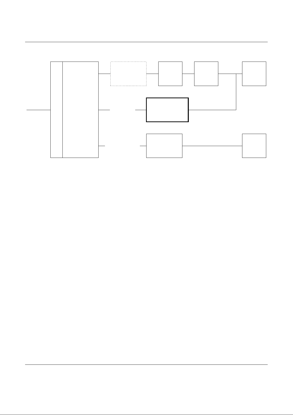
Typical Application
RS7112
Multifunction
Controller
(Ethernet MAC/V.90
Modem Combination)
P
C
I
V.90 DSP
(optional)
V.90 CODEC DAA RJ-11
CN7221
Home Networking PHY
with Inte
g
rated AFE
7-Wire Serial I/F
(7WS)
Ethernet 10 Mbps or
100 Mbps PHY/
Transceiver
Media Independent I/F
(MII)
RJ-45
LAN-056_CN7221_f1
Figure 1. Typical Application
Description
The typical application shown in Figure 1 displays a
multifunction PCI Network Interface Card (NIC). The NIC
incorporates the
RS7112
Home Networking Controller, the
CN7221
Home Networking PHY with Integrated AFE, and a
V.90 56 Kbps host-controlled modem. The
RS7112’s
7-
wire serial interface (7WS) is used to support the
CN7221
.
Home Networking
The home phoneline network is an Ethernet-compatible
LAN running over the random-tree wiring found in nearly
all homes. It does not require any hubs, routers, splitters,
filters or terminations. Initial products are PC network
interface cards, which will interface home com puters
directly to the network via an in-home telephone jack.
Home phoneline networking will also work with current
Internet access technologies, such as cable modems, V.90
and ADSL.
Page 4
LANfinity CN7221 Home Networking PHY with Integrated AFE
4
Conexant
LAN-056, Rev. A
PROPRIETARY INFORMATION
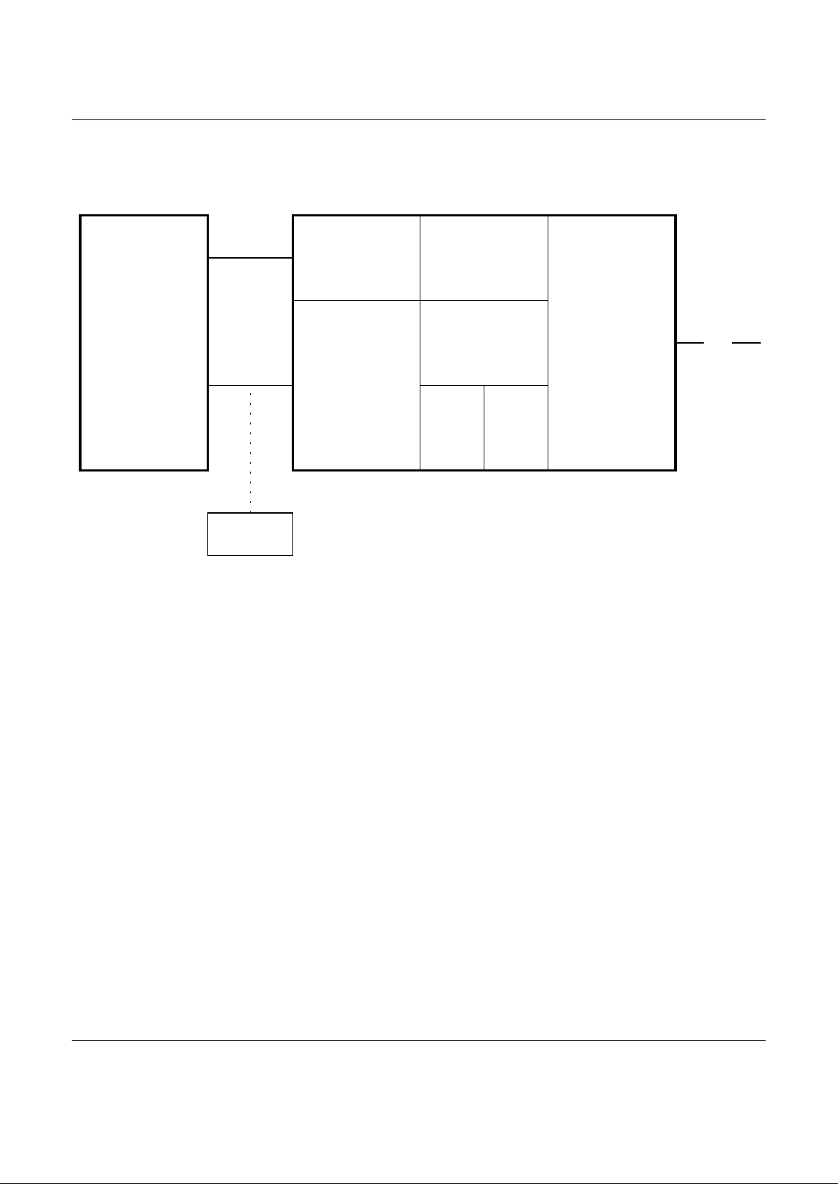
Functional Description
Interrupt Processin
g
EPROM
Interface
Registers
Physical Layer Data
Processin
g
Serial Peripheral Interface
(
SPI
)
7-Wire Serial Interface
(
7WS
)
LAN-056_CN7221_f2
Analo
g
Front End
Circuitr
y
RS7112
Bus Interface
EEPROM
CN7221 Home Networking PHY with
Integrated AFE
RJ-11
Figure 2. CN7221 Device Block Diagram
Overview
The
CN7221
PHY + AFE resides between the
RS7112
and
the physical medium and is responsible for receiving and
transmitting data on that physical medium, detecting
collisions on th e physical medium, and translating data to
and from the
RS7112
. For the purpose of this discussion,
the interface to the
RS7112
is referred to as the back end.
The discussion of the back end briefly describes the
signals involved in that interface as well as some of the
operation of those signals. More detailed information may
be gathered from the section of this document on the 7wire serial interface itself (page 5).
Back End (PHY to MAC Interface)
The back end interface is wholly defined by the seven
following signals: HLAN_TX_CLK, HLAN_TX_EN,
HLAN_TXD, HLAN_RX_CLK, HLAN_CRS, HLAN_RXD, and
HLAN_COL. The Tx signals are sampled on the falling edge
of HLAN_TX_CLK and the Rx signals are changed on the
falling edge of the HLAN_RX_CLK. HLAN_COL may change
on either edge of either the HLAN_TX_CLK or the
HLAN_RX_CLK. All signals are active high.
Due to the nature of the encoding/decoding algorithm as
well as the collision detection alg orithm used in the
CN7221,
the resulting variable bit rate forces the PHY to
“hold off” the MAC data stream by gating the
HLAN_RX_CLK and HLAN_TX_CLK signals. Gating is done
in a manner guaranteed to be glitch-free.
Page 5

Home Networking PHY with Integrated AFE LANfinity CN7221
LAN-056, Rev. A
Conexant
5
PROPRIETARY INFORMATION
System Signals
The system level signals provide hardware level
initialization, configuration and status indications from the
device. They are shown in Table 1.
The HLAN_OSC pin is the 60 MHz clock input pin.
The HLAN_IRQ signal is an active-low interrupt signal
intended for use as a level-sensitive interrupt to an external
processor. All interrupt sources are maskable and capable
of being stimulated through software via the ISR and IMR
programmable registers.
Table 1. System Signals
Signal Description
HLAN_RESET# Asynchronous system reset
HLAN_IRQ# Active low processor interrupt
HLAN_OSC 60 MHz oscillator input
Seven Wire Serial (7WS) Interface
Signals
The 7-Wire serial interface provides the digital interface to
the Ethernet MAC.
The seven signals that comprise the 7WS are
HLAN_TX_CLK, HLAN_TX_EN, HLAN_TXD,
HLAN_RX_CLK, HLAN_CRS, HLAN_RXD, and HLAN_COL.
Of these, only HLAN_TX_EN and HLAN_TXD are inputs to
the PHY; the other five are outputs from the PHY. These
signals behave differently depending on which operation is
currently happening in the PHY. The operations of the PHY
are as follows:
•
Idle (no activity in either direction)
•
RxPKT (receiving data)
•
TxPKT (transmitting data).
The subsequent subsections analyze each 7WS-related
state of the PHY in detail.
Table 2. 7WS Interface Signals
Signal Description
HLAN_TX_CLK Transmit clock
HLAN_TX_EN Transmit enable
HLAN_TXD Transmit dat a
HLAN_RX_CLK Receive clock
HLAN_CRS Receive carrier sense
HLAN_RXD Receive data
HLAN_COL Collision (active high)
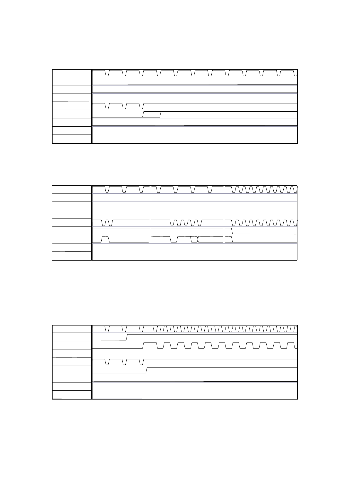
Idle State
HLAN_TX_CLK
HLAN_TX_EN
HLAN_TXD
HLAN_RX_CLK
HLAN_CRS
HLAN_RXD
HLAN_COL
HLAN_RX_CLK and HLAN_TX_CLK are synchronized to the same phase. All other signals are inactive. The two clock signals
toggle low for 116.7ns and high for 466.7ns, for an overall period of 583.3ns (about 1.7MHz).
Page 6
LANfinity CN7221 Home Networking PHY with Integrated AFE
6
Conexant
LAN-056, Rev. A
PROPRIETARY INFORMATION
RxPKT Carrier Sense Asserted
HLAN_TX_CLK
HLAN_TX_EN
HLAN_TXD
HLAN_RX_CLK
HLAN_CRS
HLAN_RXD
HLAN_COL
HLAN_RX_CLK becomes disabled (and left in the high state) as soon as HLAN_CRS is asserted. HLAN_CRS may be asserted at
a multiple of 116.7ns after the rising edge of HLAN_RX_CLK (that is, 0ns, 116.7ns, 233.3ns, 350.0ns, or 466.7ns). The clock is
re-enabled about 135 uS into the packet.
RxPKT HLAN_RX_CLK Active and HLAN_CRS Cleared
HLAN_TX_CLK
HLAN_TX_EN
HLAN_TXD
HLAN_RX_CLK
HLAN_CRS
HLAN_RXD
HLAN_COL
HLAN_RX_CLK and HLAN_TX_CLK are unrelated to each other during this time. When a symbol has been received and
decoded, HLAN_RX_CLK toggles at a rate of 233.3ns (full period, 50% duty cycle) in order to shift out the three to six bits
encoded in the symbol. The middle portion of this diagram shows the end of the preamble, followed by an SFD and the
beginning of the datagram. HLAN_CRS will fall approximately 16us after the last received symbol. Once HLAN_CRS falls,
HLAN_RX_CLK and HLAN_TX_CLK are toggled continuously at 233.3ns for 97 cycles, after which the PHY returns to the Idle
state.
TxPKT HLAN_TX_EN Asserted
HLAN_TX_CLK
HLAN_TX_EN
HLAN_TXD
HLAN_RX_CLK
HLAN_CRS
HLAN_RXD
HLAN_COL
Once HLAN_TX_EN is asserted, the PHY stops HLAN_RX_CLK, asserts HLAN_CRS, and toggles HLAN_TX_CLK at 233.3ns.
Page 7

Home Networking PHY with Integrated AFE LANfinity CN7221
LAN-056, Rev. A
Conexant
7
PROPRIETARY INFORMATION
TxPKT HLAN_RX_CLK Active
HLAN_TX_CLK
HLAN_TX_EN
HLAN_TXD
HLAN_RX_CLK
HLAN_CRS
HLAN_RXD
HLAN_COL
HLAN_TX_CLK continues to toggle at 233.3ns until the SFD is observed, as shown in the first section of the above diagram. At
this point, HLAN_TX_CLK is disabled (high) until the AID header has been transmitted on the wire (or until a HLAN_COL has
been detected). This takes about 120us, at which time HLAN_RX_CLK starts toggling, thereby shifting 32 bits of preamble and
SFD back to the MAC. Sometime later, the HLAN_TX_CLK restarts as symbols get sent onto the wire in an analogous manner
as HLAN_RX_CLK during packet reception.
TxPKT HLAN_TX_EN Cleared
HLAN_TX_CLK
HLAN_TX_EN
HLAN_TXD
HLAN_RX_CLK
HLAN_CRS
HLAN_RXD
HLAN_COL
Once HLAN_TX_EN is cleared, the last symbol gets encoded and transmitted, the looped-back data is presented back to the
MAC, and about 22us later, HLAN_CRS falls. Once HLAN_CRS falls, HLAN_TX_CLK and HLAN_RX_CLK toggle with a period of
233.3ns for 97 clocks, after which the system returns to the Idle state.
Page 8

LANfinity CN7221 Home Networking PHY with Integrated AFE
8
Conexant
LAN-056, Rev. A
PROPRIETARY INFORMATION
TxPKT HLAN_COL Asserted
HLAN_TX_CLK
HLAN_TX_EN
HLAN_TXD
HLAN_RX_CLK
HLAN_CRS
HLAN_RXD
HLAN_COL
HLAN_COL will be asserted some time after the preamble and SFD have been clocked in. HLAN_TX_CLK and HLAN_RX_CLK
are then clocked with a period of 233.3ns until HLAN_CRS drops. HLAN_TX_EN drops about 32 clocks after HLAN_COL was
asserted. HLAN_CRS and HLAN_COL are dropped together after more than 500 clocks (about 120us). HLAN_TX_CLK and
HLAN_RX_CLK keep toggling at 233.3ns period for roughly another 100 clock cycles, when the system returns to the idle state.
RxPKT HLAN_COL Asserted
HLAN_TX_CLK
HLAN_TX_EN
HLAN_TXD
HLAN_RX_CLK
HLAN_CRS
HLAN_RXD
HLAN_COL
HLAN_COL may be asserted up to 120us after HLAN_CRS has been asserted. Once HLAN_COL has been asserted,
HLAN_TX_CLK and HLAN_RX_CLK run at a period of 233.3ns per cycle until 97 cycles after HLAN_COL and HLAN_CRS are
cleared. It can take up to about 60us for HLAN_CRS to clear.
Page 9

Home Networking PHY with Integrated AFE LANfinity CN7221
LAN-056, Rev. A
Conexant
9
PROPRIETARY INFORMATION
Serial Peripheral Interface
The SPI provides a software interface for configuration and
status of the
CN7221
.
The SPI signals are composed of: HLAN_SPI_CLK,
HLAN_SPI_DOUT, HLAN_SPI_DIN, and HLAN_SPI_CS#.
Commands are issued to the device by asserting the
HLAN_SPI_CS# signal (active low), shifting in an eight-bit
opcode; if the operation is a read or a write, the opcode is
followed by an eight-bit register address. If the operation is
a write, the address is followed by an eight-bit data byte. If
the operation is a read, the HLAN_SPI_DOUT pin will shift
out an eight bit data byte representing the contents of the
register referenced by the address field. All commands
must be initiated with a high-to-low transition on the
HLAN_SPI_CS# pin. The device also may be commanded
to set or clear its WE flag. This flag is cleared upon reset,
and disables all write operations when in that state.
Opcodes are as follows:
0000 0110 SET WE
0000 0100 CLEAR WE
0000 0011 READ
0000 0010 WRITE
Timing for the various signals in SPI mode is defined in
Table 4 and in Figure 3.
The HLAN_SPI_DIN signal should not be changed until at
least 100ns after the rising edge of HLAN_SPI_CLK. In
other words, the HLAN_SPI_DIN signal has a hold time
constraint of 100ns past the rising edge of
HLAN_SPI_CLK.
Table 3. SPI Signals
Signal Description
HLAN_SPI_CLK Serial interface cloc k
HLAN_SPI_DOUT Serial data output
HLAN_SPI_DIN Serial data input
HLAN_SPI_CS# Serial interface c hi p select (active l ow)
Table 4. SPI Timing
Mnemonic Description Min Max Units
TWIDTHclkl Positive half-cycle
pulse width
400 ns
TWIDTHclkh Negative half-cycle
pulse width
400 ns
TSETcsl CSN low to rising
clock edge
50 ns
TSETcsh CSN high to rising
clock edge
50 ns
TDLYsov Falling clock edge to
SO valid
50 ns
TDLYsoz Falling clock edge to
SO tri-state
100 ns
TSETsiv SI valid to rising
clock edge
50 ns
CLK
CSN
HLAN_SPI_DIN
HLAN_SPI_DOU
TSETcsl
TWIDTHclkh
TWIDTHclkl
TSETsiv
TDLYsov
TSETcsh
TDLYsoz
b7 b6 b5 b4 b3 b2 b1 b0 b7 b6 b5 b4 b3
Instruction Byte
b2 b1 b0 b7 b6 b5 b4
b7 b6 b5 b4
Address Byte
b3 b2 b1 b0
Data Byt e (don't-c are w h en r ead i ng)
Data Byte (high-Z when writing)
b3 b2 b1 b0
Figure 3. SPI Timing
Page 10

LANfinity CN7221 Home Networking PHY with Integrated AFE
10
Conexant
LAN-056, Rev. A
PROPRIETARY INFORMATION
LANfinity RS7112 Interface
The
RS7112
interface consists of the SPI signals (see page
9), and the HLAN_IRQ# signal.
All SPI registers in the system are readable and writable.
The TxSPEED, TxPOWER, and CMDignore bits of the
CONTROL register may be set or cleared in two ways: SPI
CONTROL register write or remote management command
(TxSPEED and TxPOWER only). These methods may
overwrite one another. After reset, any change in the state
of those pins will update the CONTROL register bits.
Table 5. RS7112 Interface Signals
Signal Description
HLAN_IRQ# Active low processor interrupt
Remote Commands
Any node in a home phoneline network may issue remote
commands. The effect of a remote command is to set the
transmit speed and power of all nodes in the network. A
remote command is encoded in the AID header and is
identified by having an AID address of 0xFF. The remaining
AID header information contains the commanded power
and speed. Three identical remote commands must be
received before a PHY will respond by changing its’
transmit speed and power. Once three identical remote
commands have been received, however, the transmit
speed and power are updated and bit 1 of the ISTAT
register is set.
The PHY will issue thr e e remote comma nds when any o ne
of bits 8 through 11 of the CONTROL register is set. As
soon as these bits are set, the PHY will automatically
update it’s own transmit speed and power and start issuing
the remote command on subsequent packets until three
packets have been successfully transmitted (that is,
without collision). Once the thr e e remote comma nds have
been sent, bits 8 through 11 of the CONTROL register will
be cleared and bit 0 of the ISTAT register will be set.
Page 11

Home Networking PHY with Integrated AFE LANfinity CN7221
LAN-056, Rev. A
Conexant
11
PROPRIETARY INFORMATION
Pinout Diagram
1
2
3
4
5
6
7
8
9
10 11 12 13 14 15 16
24
23
22
21
20
19
18
17
32 31 30 29 28 27 26 25
HLAN_OSC
HLAN_SPI_DOUT
HLAN_SPI_CS#
HLAN_SPI_CLK
HLAN_SPI_DIN
HLAN_RESET#
VSS
AFE_REF_DATA
AFE_RBIAS
AFE_VDD_RX
AFE_VSS_RX
AFE_VC
AFE_VSS_TX
AFE_RX_MINUS
AFE_RX_PLUS
AFE_TX_MINUS
AFE_TX_PLUS
VDD
SCAN_ENABLE
SCAN_MODE
HLAN_IRQ#
HLAN_RXD
HLAN_RX_CLK
HLAN_COL
HLAN_CRS
VDD
HLAN_TX_CLK
HLAN_TXD
AFE_REF_NOISE
AFE_REF_PEAK
HLAN_TX_EN
VSS
Figure 4. CN7221 32-pin TQFP Pinout Diagram
Page 12

LANfinity CN7221 Home Networking PHY with Integrated AFE
12
Conexant
LAN-056, Rev. A
PROPRIETARY INFORMATION
Pin Designations by Number
Table 6. CN7221 32-pin TQFP Pin Designations by Number
Pin No. Signal Pin No. Signal
1 HLAN_OSC 17 AFE_TX_MINUS
2 HLAN_SPI_DOUT 18 AFE_TX_PLUS
3 HLAN_SPI_CS# 19 VDD
4 HLAN_SPI_CLK 20 SCAN_ENABLE
5 HLAN_RESET# 21 SCAN_MODE
6 VSS 22 HLAN_IRQ#
7 AFE_REF_NOISE 23 HLAN_RXD
8 AFE_REF_PEAK 24 HLAN_RX_CLK
9 AFE_REF_DATA 25 HLAN_COL
10 AFE_VDD_RX 26 HLAN_CRS
11 AFE_VSS_RX 27 HLAN_TX_EN
12 AFE_RBIAS 28 VSS
13 AFE_VC 29 VDD
14 AFE_VSS_TX 30 HLAN_TXD
15 AFE_RX_MINUS 31 HLAN_TX_CLK
16 AFE_RX_PLUS 32 HLAN_SPI_DIN
Page 13

Home Networking PHY with Integrated AFE LANfinity CN7221
LAN-056, Rev. A
Conexant
13
PROPRIETARY INFORMATION
Pin Designations by Group
Table 7. Pin Designations by Group
Home LAN
Pin Name Type Schmitt Resistive Drive Description Pin Number(s)
HLAN_OSC I CMOS 60 MHz oscillator input 1
HLAN_RESET# I
↓
25Kohm
CMOS Active high asynchronous s ystem reset 5
HLAN_IRQ# O 6mA Active low processor interrupt 22
HLAN_TX_EN I
↓
25Kohm
CMOS 7WS transmit enable 27
HLAN_TXD I
↓
25Kohm
CMOS 7WS transmit data 30
HLAN_TX_CLK O 6mA 7WS transmit clock 31
HLAN_COL O 6mA 7WS collision (active high) 25
HLAN_CRS O 6mA 7WS receive carrier sense 26
HLAN_RXD O 6mA 7W S receive data 23
HLAN_RX_CLK O 6mA 7WS receive cl ock 24
HLAN_SPI_CS# I/O
↑
100Koh
m
6mA Serial interface chip select
Active low
3
HLAN_SPI_CLK I/O 6mA Serial interface clock 4
HLAN_SPI_DOUT O 6mA Serial data output 2
HLAN_SPI_DIN I CMOS Serial data input 32
AFE Interface (Reference)
Pin Name Type Schmitt Resistive Drive Description Pin Number(s)
AFE_REF_NOISE Noise reference filtered with an external 0.0075
uF Cap for data CT comparator.
7
AFE_REF_PEAK Peak reference filtered with an external 0.0034 uF
Cap for peak CT comparator.
8
AFE_REF_DATA Data referenc e f i l tered with an external 0.0134 uF
Cap for data CT comparator.
9
AFE_RBIAS External 1% 2.75kOhm resis tor to set reference
current.
12
AFE_RX_MINUS Negative input of the 7.5MHz receive signal 15
AFE_RX_PLUS Positive input of the 7.5MHz rec ei ve s i gnal 16
AFE_TX_MINUS Negative output of the 7.5MHz TX signal
connected to the 50ohm resi stor and 1000pF AC
coupling Caps.
17
AFE_VDD_RX RX power supply (3-3.6V or 3.15-3.45) 10
AFE_VSS_RX RX ground 11
AFE_VSS_TX TX ground 14
AFE_VC Middle point of the power supply filtered with an
external 10uF Cap.
13
AFE_TX_PLUS Positive output of the 7. 5MHz TX signal
connected to the 50ohm resi stor and 1000pF AC
coupling Caps.
18
Page 14

LANfinity CN7221 Home Networking PHY with Integrated AFE
14
Conexant
LAN-056, Rev. A
PROPRIETARY INFORMATION
Test Signals
Pin Name Type Schmitt Resistive Drive Description Pin Number(s)
SCAN_MODE I
8
↓
Selects different scan modes 21
SCAN_ENABLE I
8
↓
Scan enable (1 = enable scan) 20
Power Pins
Pin Name Type Characteristic Description Pin Number(s)
VDD P
5 pins
+3.3V Power 19, 29
VSS G
7 pins
Ground 6, 28
Page 15

Home Networking PHY with Integrated AFE LANfinity CN7221
LAN-056, Rev. A
Conexant
15
PROPRIETARY INFORMATION
Electrical Characteristics
Table 8.Absolute Maximum Ratings
Parameter Symbol Min Typ Max Units
Supply Voltage V
DD
V
Input Voltage V
IN
V
Operating Temperature Range T o
C
Storage Temperature T
stg
o
C
Voltage Applied to Outputs i n Hi gh Z state V
hz
V
DC Input Clamp Current I
lk
mA
DC Input Clamp Current I
ok
mA
Static Discharge Vol tage (25 oC)
ESD V
Latch-up Current I
trig
mA
Table 9. DC Electrical Characteristics
TA
= 0oC to +70oC, VDD = +3.3V ± 5%, VSS = 0V.
Parameter Symbol Min Typ Max Units
Input Voltage Low V
IL
V
Input Voltage High V
IH
V
Output Voltage Low @ IOL = 2, 4, 8, 12 mA V
OL
V
Output Voltage High @ IOH = 2, 4, 8, 12 mA V
OH
V
Table 10. AC Electrical Characteristics
TA = 0oC to +70oC, VDD = +3.3V ± 5%, VSS = 0V.
Parameter Symbol Min Typ Max Units
Frequency (PCI_CLK) f
pck
MHz
Frequency (8023_MII_TX_CLK) 100 Mbps f
xtal
MHz
Frequency (8023_MII_RX_CLK) 100 Mbps TB D MHz
Frequency (8023_MII_TX_CLK) 10 Mbps TBD MHz
Frequency (8023_MII_RX_CLK) 10 Mbps TBD MHz
Frequency (8023_MII_MDC) TBD MHz
Note
: Setup, Hold and Delays are with respect to the rising edge of the respective clock unless specified. PCI Bus signals
conform to the PCI Bus Timing Specification.
Page 16

LANfinity CN7221 Home Networking PHY with Integrated AFE
16
Conexant
LAN-056, Rev. A
PROPRIETARY INFORMATION
Table 11. Current and Power Characteristics
Mode Typical Current
(mA)
Maximum
Current (mA)
Typical Power
(W)
Maximum
Power
(W)
Notes
Active
Idle
Power down
Page 17

Home Networking PHY with Integrated AFE LANfinity CN7221
LAN-056, Rev. A
Conexant
17
PROPRIETARY INFORMATION
Package Dimensions
DETAIL A
A1
L1
c
L
A
D1
A2
Millimeters
0.05
8.75
0.5
0.30
0.13
1.6 MAX
0.15
1.4 REF
9.25
7.0 REF
5.6 REF
0.75
1.0 REF
0.80 BSC
0.40
0.19
0.10 MAX
0.0020
0.3445
0.0197
0.0118
0.0051
A
A1
A2
D
D1
D2
L
L1
e
b
c
Coplanarity
Min.
Max.
Min.
Max.
Inches*
Dim.
Ref: 32-PIN TQFP (GP00-D262)
* Metric values (millimeters) should be used for
PCB layout. English values (inches) are
converted from metric values and may include
round-off errors.
0.0630 MAX
0.0059
0.0551 REF
0.3642
0.2756 REF
0.2205 REF
0.0295
0.0394 REF
0.0315 BSC
0.0157
0.0075
0.004 MAX
PD-TQFP-32 (040395)
DETAIL A
D1
e
b
D
D2
D1
D1
D
D2
PIN 1
REF
Figure 5. 32-pin TQFP Package Dimensions
Page 18

Further Information
literature@conexant.com
1-800-854-8099 (NorthAmerica)
33-14-906-3980 (International)
Web Site
www.conexant.com
World Headquarters
Conexant Systems, Inc.
4311 Jamboree Road
P. O. Box C
Newport Beach, CA
92658-8902
Phone: (949) 483-4600
Fax: (949) 483-6375
U.S. Florida/South America
Phone: (727) 799-8406
Fax: (727) 799-8306
U.S. Los Angeles
Phone: (805) 376-0559
Fax: (805) 376-8180
U.S. Mid-Atlantic
Phone: (215) 244-6784
Fax: (215) 244-9292
U.S. North Central
Phone: (630) 773-3454
Fax: (630) 773-3907
U.S. Northeast
Phone: (978) 692-7660
Fax: (978) 692-8185
U.S. Northwest/Pacific West
Phone: (408) 249-9696
Fax: (408) 249-7113
U.S. South Central
Phone: (972) 733-0723
Fax: (972) 407-0639
U.S. Southeast
Phone: (919) 858-9110
Fax: (919) 858-8669
U.S. Southwest
Phone: (949) 483-9119
Fax: (949) 483-9090
APAC Headquarters
Conexant Systems Singapore, Pte.
Ltd.
1 Kim Seng Promenade
Great World City
#09-01 East Tower
SINGAPORE 237994
Phone: (65) 737 7355
Fax: (65) 737 9077
Australia
Phone: (61 2) 9869 4088
Fax: (61 2) 9869 4077
China
Phone: (86 2) 6361 2515
Fax: (86 2) 6361 2516
Hong Kong
Phone: (852) 2827 0181
Fax: (852) 2827 6488
India
Phone: (91 11) 692 4780
Fax: (91 11) 692 4712
Korea
Phone: (82 2) 565 2880
Fax: (82 2) 565 1440
Phone: (82 53) 745 2880
Fax: (82 53) 745 1440
Europe Headquarters
Conexant Systems France
Les Taissounieres B1
1681 Route des Dolines
BP 283
06905 Sophia Antipolis Cedex
FRANCE
Phone: (33 4) 93 00 33 35
Fax:(334)93003303
Europe Central
Phone: (49 89) 829 1320
Fax: (49 89) 834 2734
Europe Mediterranean
Phone: (39 02) 9317 9911
Fax: (39 02) 9317 9913
Europe North
Phone: (44 1344) 486 444
Fax: (44 1344) 486 555
Europe South
Phone: (33 1) 41 44 36 50
Fax:(331)41443690
Middle East Headquarters
Conexant Systems
Commercial (Israel) Ltd.
P. O. Box 12660
Herzlia 46733, ISRAEL
Phone: (972 9) 952 4064
Fax: (972 9) 951 3924
Japan Headquarters
Conexant Systems Japan Co., Ltd.
Shimomoto Building
1-46-3 Hatsudai,
Shibuya-ku,Tokyo
151-0061 JAPAN
Phone: (81 3) 5371-1567
Fax: (81 3) 5371-1501
Taiwan Headquarters
Conexant Systems, Taiwan Co., Ltd.
Room 2808
InternationalTrade Building
333 Keelung Road, Section 1
Taipei 110, TAIWAN, ROC
Phone: (886 2) 2720 0282
Fax: (886 2) 2757 6760
 Loading...