

Page 1

Circuit Note
CN-0281
Rev. 0
engineers. Standard engineering practices have been employed in the design and construction of
each circuit, and their function and performance have been tested and verified in a lab environment at
However, you are solely responsible for testing the circuit and determining its
suitability and applicability for your use and application. Accordingly, in no event shall Analog Devices
whatsoever connected to the use of any Circuits from the Lab circuits. (Continued on last page)
Fax: 781.461.3113 ©2012 Analog Devices, Inc. All rights reserved.
Devices Connected/Referenced
ADuC7060/
Circuits from the Lab™ reference circuits are engineered and
tested for quick and easy system integration to help solve today’s
analog, mixed-signal, and RF design challenges. For more
information and/or support visit www.analog.com/CN0281.
ADuC7061
ADT7311
AD8628 Precision, Low Power, Zero Drift Op Amp
ADP7102 Low Dropout Linear Regulator
Automotive SENT Interface-Based Thermocouple Temperature Sensor with Cold Junction
Compensation Using the ADuC7060/ADuC7061 Precision Analog Microcontroller
EVALUATION AND DESIGN SUPPORT
Design and Integration Files
Schematic, Layout Files, Source Code
CIRCUIT FUNCTION AND BENEFITS
This circuit uses the ADuC7060 or the ADuC7061 precision
analog microcontroller in an accurate thermocouple temperature
monitoring application. The ADuC7060/ADuC7061 integrate
dual 24-bit sigma-delta (Σ-Δ) analog-to-digital converters (ADCs),
dual programmable current sources, a 14-bit digital-to-analog
converter (DAC), and a 1.2 V internal reference, as well as an
ARM7 core, 32 kB flash, 4 kB SRAM, and various digital peripherals
such as UART, timers, serial peripheral interface (SPI), and I
interfaces.
In the circuit, the ADuC7060/ADuC7061 are connected to a
thermocouple and a 100 Ω platinum resistance temperature
detector (RTD). The RTD is used for cold junction compensation.
As an extra option, the ADT7311 digital temperature sensor
can be used to measure the cold junction temperature instead of
the RTD.
In the source code, an ADC sampling rate of 4 Hz was chosen.
When the ADC input programmable gain amplifier (PGA) is
configured for a gain of 32, the noise-free code resolution of the
ADuC7060/ADuC7061 is greater than 18 bits.
The single edge nibble transmission (SENT) interface to the host
is implemented by using a timer to control a digital output pin.
This digital output pin is then level shifted externally to 5 V using
an external NPN transistor. An EMC filter is provided on the
SENT output circuit as recommended in Section 6.3.1 of the SENT
protocol (SAE J2716 Standard). The data is measured as falling
edge to falling edge, and the duration of each pulse is related to the
number of system clock ticks. The system clock rate is determined
by measuring the SYNC pulse. The SYNC pulse is transmitted
2
C
at the start of every packet. More details are provided in the
SENT Interface section.
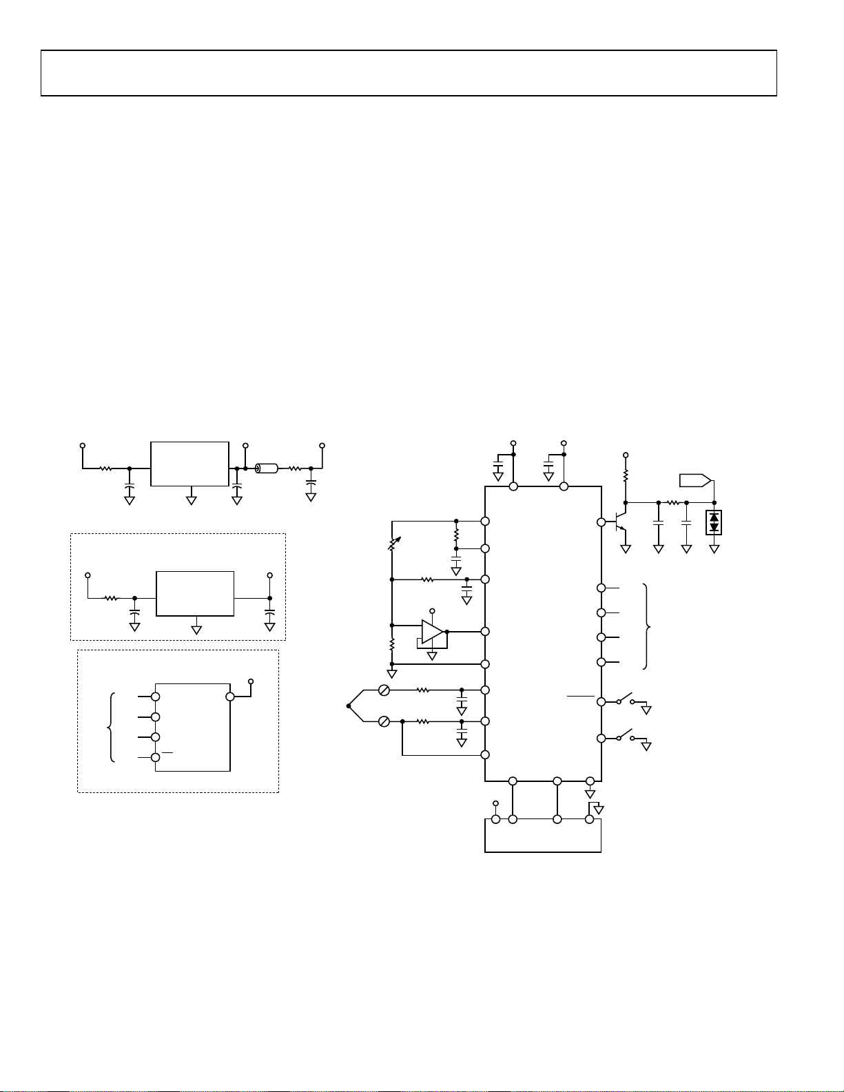
CIRCUIT DESCRIPTION
The following features of the ADuC7060/ADuC7061 are used
in this application:
• A primary, 24-bit Σ-Δ ADC with a PGA. The PGA is set
for a gain of 32 in the software for this application. The
primary ADC was switched continuously between
sampling the thermocouple and the RTD voltages.
• If an RTD is used for measuring the cold junction temperature,
programmable excitation current sources force a controlled
current through the RTD. The dual current sources are
configurable in 200 µA steps from 0 µA to 2 mA. For this
example, a 200 µA setting was used to minimize the error
introduced by the RTD self-heating.
• If the ADT7311 is used for measuring the cold junction
temperature, the SPI interface is used in master mode to
connect the ADT7311 slave device.
• An internal 1.2 V reference for the ADC in the ADuC7060/
ADuC7061. For measuring the thermocouple voltage, the
internal voltage reference was used due to its precision.
• An external voltage reference for the ADC in the ADuC7060/
ADuC7061. For measuring the RTD resistance, a ratiometric
setup was used where an external reference resistor (R
was connected across the external VREF+ and VREF− pins.
• The AD8628 si
high impedance reference voltage across R
• The OP193 is another option instead of the AD8628.
• A DAC that was used to set the thermocouple common-
mode voltage to 850 mV above ground.
ARM7-Based Microcontroller with Dual
24-Bit Σ-Δ ADCs
±0.5°C Accurate ,16-Bit Digital SPI
Temperature Sensor
ngle supply op amp was used to buffer the
to the ADC.
REF
REF
)
Circuits from the Lab™ circuits from Analog Devices have been designed and built by Analog Devices
room temperature.
be liable for direct, indirect, special, incidental, consequential or punitive damages due to any cause
One Technology Way, P.O. Box 9106, Norwood, MA 02062-9106, U.S.A.
Tel: 781.329.4700
www.analog.com
Page 2
CN-0281 Circuit Note
5V
PWRIN
5V
PWRIN
10Ω 1.6Ω
10Ω
10Ω
10Ω
10Ω
10kΩ
C1R1C2
100Ω
Pt RTD
R
REF
5.6kΩ
(0.1%)
THERMOCOUPLE
JUNCTION
2.5V
0.1µF 4.7µF
0.1µF
0.1µF
0.1µF
0.1µF
0.1µF
0.1µF
PWRIN
AD8628
ADuC7016
5V
AVDD
AVDD
DVDD
BEAD
VIN
ADP7102
(ADJ)
VOUT
GND
ONLY REQUIRED FOR ADT7311
TEMPERATURE SENSOR OPTION
AVDD
AVDD
PWRIN
10Ω
0.1µF
P0.0 SCLK
0.1µF
2.7V
VIN
ADP7102
(ADJ)
ADT7311
VOUT
GND
IEXC0
ADC0
ADC1
VREF+
VREF–
P0.0
P0.4
PESD1LIN
P0.1
SPI
P0.2
P0.3
S2
S1
ADC2
ADC3
RESET
NTRST
DAC0
P1.0/SIN
PROGRAMMABLE
INTERFACE
P1.1/SOUT GND
V
DD
2.7V
P0.1
SPI
DOUT
P0.2 DIN
P0.3 CS
0.1µF
DVDD
DVDD
2N3904
SENT
10889-001
• An AR M7 TDMI® co re. The powerful 16-/32-bit A RM7 c ore
with integrated 32 kB flash and SRAM memory runs the
us er code that configures and controls the ADC, processes
the ADC conversions from the RTD, and controls the
com mu nicatio ns o ver t he S PI inte rfa ce.
• Timer1 and a digital output pin are use d to generate the
SENT output signal.
• An optional PESDLIN protection diode for suppression of
ESD, electrical fast transients (EFT), and surge transients
up to 23 k V.
• An EMC f ilte r on the SENT output as recommended in
Section 6.3.1 of the SAE J2716 standard (SENT Protocol).
• Two external switches are used to force the part into its
flash boot mode. By holding S1 low and toggling S2, the
ADuC7060/ADuC7061 e nter boot m ode instead of normal
user m ode. In boot mode, the internal flash can be
reprogrammed through the UART interface.
Bo th t he thermocouple and th e RTD generate ver y small s ignals;
therefore, a PGA is required to amplify those signals. As the
au xiliar y AD C on the ADuC7060/ADuC7061 does not have a
PGA, both were connected to the primary ADC, and switching
between the two was done in software.
The th erm oco uple u sed in this a pplicatio n is a Type T (copperco nst antan ), w hich has a t emperatu re range of −200°C t o + 350°C.
Its sens itivity is approximately 40 µV/°C; the refore, in bipo lar
mode, the ADC , with a PGA g ain o f 32, can cover the entire
temperature range of the thermocouple.
Th e RTD was us ed for cold ju nction compensat ion. In this circuit,
a platinum, 100 Ω RTD, Enercorp PC S 1.1503.1 was used. It is
available in a 0805 surface-mount package. This RTD has a
temperature variation of 0.385 Ω/°C.
Note that the reference resistor, R
, s hou ld be a p recis ion
REF
5.6 kΩ (±0.1%).
Fi gure 1. ADuC7060/ADuC7061 as a Temperature Monitor Controller with a Thermocouple Interface (Simplified Schematic, All Connections Not Shown)
Rev. 0 | Pag e 2 of 6
Page 3

Circuit Note CN-0281
0
56
CLOCK TICKS
SYNC
PULSE
STATUS
PULSE
D1 TO D6 CRC
PULSE
1 0 7 1 2 8 0
10889-002
0.30
0.25
0.20
0
0.05
0.10
0.15
–0.05
–210 –140 –70 0 70 140 210 280 350
ERROR (°C)
TEMPERATURE (°C)
10889-003
SENT Interface
The SENT interface is a single pin, unidirectional (sensor to host),
time modulated signal used mainly in automotive systems for
interfacing distributed sensors to host CPUs.
The main requirements for SENT include the following:
• It must have a 0 V to 5 V signal swing with EMC filtering.
• The clock used for the SENT signal must be accurate to ±20%.
• The SENT output circuit must be robust enough to tolerate
short circuit to ground and short circuit to supply voltages.
The associated source code uses the P0.4 digital pin of the
ADuC7061 as the SENT output pin. The packet format used is
the single sensor packet format as detailed in A.4 section of the
SAE J2716 standard (SENT Protocol) document. The source
code, particularly the SENT.h and Sent.c files can be modified to
support other packet formats. The overall temperature result is
returned in /°C format in Data Nibble 1 to Data Nibble 3. In
summary, the returned output packet is
• 56 clock ticks for sync pulse
• Status pulse (7 ticks to 15 ticks)
• Data Nibble 1 (Bit 11 to Bit 8 of the temperature result)
• Data Nibble 2 (Bit 7 to Bit 4 of the temperature result)
• Data Nibble 3 (Bit 3 to Bit 0 of the temperature result)
• Data Nibble 4 (Bit 7 to Bit 4 of the counter)
• Data Nibble 5 (Bit 3 to Bit 0 of the counter)
• Data Nibble 6 (inverse of Nibble 1)
An example packet is shown in Figure 2.
Code Description
Timer1 is used to control the SENT output pin, P0.4. When a
temperature result is been calculated from the ADC results for
the thermocouple and the cold junction temperature, the SENT
packet structure, SENT_PACKET, is updated, and Timer1 started.
The fields of the structure are clocked out on the P0.4 pin, as
shown in Figure 2. The first stage of the packet is the sync sequence.
The host determines the clock period from this pulse, and it
determines the subsequent nibble values from this.
To get a temperature reading, measure the temperature of the
thermocouple and the RTD. The RTD temperature is converted
to its equivalent thermocouple voltage via a lookup table. These
two voltages are added together to give the absolute value of the
voltage at the thermocouple.
First, the voltage between the two wires of the thermocouple (V1)
is measured. Then, the RTD voltage is measured and converted to
a temperature via a lookup table. This temperature is then
converted to its equivalent thermocouple voltage (V2). V1 and
V2 are then added to give the overall thermocouple voltage, and
this value is then converted to the final temperature measurement.
A piecewise linearization scheme is used to calculate the final
temperature value. The respective temperatures for a fixed number
of voltages are stored in an array, and values in between are
calculated using a linear interpolation between the adjacent points.
Figure 3 gives the algorithm error using the ideal thermocouple
voltages. Figure 4 shows the error obtained when using the
ADC0 pin on the ADuC7060/ADuC7061 to measure the
52 thermocouple voltages over the full thermocouple
operating range. The overall worst-case error is <1°C.
Figure 2. Example SENT Packet Measured at the P0.4 Pin
The circuit must be constructed on a multilayer printed circuit
board (PCB) with a large area ground plane. Proper layout,
grounding, and decoupling techniques must be used to achieve
optimum performance (see Tu tor i al M T-031, Grounding Data
Converters and Solving the Mystery of "AGND" and "DGND,"
Tutor ia l MT-101, Decoupling Techniques, and the ADuC7060/
ADuC7061 evaluation board layouts).
Figure 3. Error When Using Piecewise Linear Approximation Using
Rev. 0 | Page 3 of 6
52 Calibration Points and Ideal Measurements
Page 4

CN-0281 Circuit Note
0
0.1
0.2
0.3
0.4
0.5
0.6
0.7
0.8
0.9
1.0
–210 –140 –70 0 70 140 210 280 350
ERROR (°C)
TEMPERATURE (°C)
10889-004
10889-005
Figure 4. Error When Using Piecewise Linear Approximation Using
52 Calibration Points Measured by the ADC0 Pin of the
The RTD temperature is calculated using lookup tables and is
implemented for the RTD the same way as for the thermocouple.
Note that the RTD has a different polynomial describing its
temperatures as a function of resistance.
The source code in the design support package was generated using
KEIL µVision V3.90.
For details on linearization and maximizing the performance of
the RTD, refer to Application Note AN-0970, RTD Interfacing
and Linearization Using an ADuC706x Microcontroller.
COMMON VARIATIONS
Instead of using an external RTD, the ADT7311 temperature
sensor can be used to measure the cold junction temperature.
Source code using the ADT7311 is provided with the software
package in the design support package:
www.analog.com/CN0281-DesignSupport.
An extra external regulator is required to power the ADT7311.
The ADP7102 was used in this circuit, but an alternative is the
ADP120.
If more GPIO pins are required on the microcontroller, the
ADuC7060, which comes in a 48-lead LFCSP or a 48-lead L Q FP,
is another option. Note that the ADuC7060/ADuC7061 can be
programmed or debugged via a standard JTAG interface.
When using the external reference resistor as the reference source
for the RTD measurement, it is recommended to buffer the input
to the VREF+ pin using an op amp in unity-gain mode. This is to
ensure that the input leakage current to the VREF+ pin does
not distort the measurement accuracy. In Figure 9, the OP193
was used for this purpose. Figure 1 shows the AD8628 which is
characterized to work in the −40°C to +150°C operating range.
ADuC7060/ADuC7061
For a wider temperature range, a different thermocouple can be
used, such as a Type J. To minimize the cold junction compensation
error, a thermistor can be placed in contact with the actual cold
junction instead of on the PCB.
Instead of using the RTD and external reference resistor for
measuring the cold junction temperature, an external digital
temperature sensor can be used. For example, the ADT7311
can connect to the ADuC7060/ADuC7061 via the I
2
C interface.
For additional information on cold junction compensation, see
the Sensor Signal Conditioning, Analog Devices, Chapter 7,
"Temperature Sensors."
CIRCUIT EVALUATION AND TEST
Rev. 0 | Page 4 of 6
SENT Interface Tests
The SENT interface output was evaluated using a digital oscilloscope and a logic analyzer. The SENT interface was only tested
with a SENT clock period of 100 µs, which is the maximum
allowed by the SENT standard. The limiting factors in this
implementation include the following:
• Variation in FIQ interrupt latency for the timer. The interrupt
latency of an ARM7 can be up to 45 CPU clocks. With a
10.24 MHz CPU clock, this is up to 4.4 µs. The minimum
is 5× CPU clocks (0.5 µs). The worst-case latency occurs
when the ARM7 core is executing a LDMIA or STMIA (load
or store multiple values to/from memory). Select the Split
Load and Store Multiple compiler option to minimize this,
and see
Figure 5 to see
how to do this.
• The 10.24 MHz oscillator on the ADuC7060/ADuC7061
has a worst-case accuracy of ±3% over the −40°C to +125°C
operating temperature range.
Figure 5. Selecting Split Load and Store Multiple Option
Despite these limitations, this implementation is well within the
required ±20% timing accuracy of the SENT specification when
a SENT clock period of 100 µs is selected.
Page 5

Circuit Note CN-0281
4.5
4.0
3.5
3.0
2.
5
2.0
AMPLITUDE (V)
TIME (µs)
1.5
1.0
0.5
5 10 15 20 25 30 35 400
0
10889-006
EVAL-ADuC7061MKZ
WAVTEK 4808
MULTIFUNCTION
CALIBRATOR
PC
J2-9
J2-8
J2-5
THERMOCOUPLE
JUNCTION
SEE TEXT
USB
CABLE
10889-007
0
–0.01
–25 –5
ERROR (°C)
TEMPERATURE (°C)
–0.02
–0.03
–0.04
–0.05
–0.06
–0.07
–0.08
–0.09
–0.10
15 35 55
75 95 115
10889-009
An EMC filter has been catered for on the SENT output in Figure 1.
Chose values for this filter (R1, C1, C2) to meet the targeted
transmitter output waveform, as shown in Figure 6, to reduce
EMC emissions due to the SENT output.
Only limited testing of this filter has been done; therefore, the
resistor and capacitor values for the output filter were omitted,
as is shown in Figure 1 (R1, C1, and C2).
Figure 6. Example SENT Shaped Waveform Transmitter Output
To further test and evaluate the circuit, the thermocouple
measurements and the RTD measurements were evaluated
separately.
Thermocouple Measurement Test
The basic test setup is shown in Figure 7. Two methods were
used to evaluate the performance of the circuit. Initially, the
circuit was tested with the thermocouple attached to the board
and used to measure the temperature of an ice bucket, and then
the temperature of boiling water.
A Wavetek 4808 multifunction calibrator was used to fully
evaluate the error, as shown in Figure 3 and Figure 4. In this
mode, the thermocouple was replaced with the calibrator as the
voltage source, as shown in Figure 7. To evaluate the entire range
of a Type T thermocouple, the calibrator was used to set the
equivalent thermocouple voltage at 52 points between −200°C
to +350°C for the negative and positive ranges of the Type T
thermocouple (see the ITS-90 Table for Type T thermocouple).
To evaluate the accuracy of the lookup algorithm, 551 voltage
readings, equivalent to temperatures in the range of −200°C to
+350°C spaced at +1°C, were passed onto the temperature
calculation functions. Errors were calculated for the linear method
and the piecewise linear approximation method as can be seen
in Figure 3
and Figure 4.
RTD Measurement Test
To evaluate the RTD circuit and linearization source code, the
RTD on the board was replaced with an accurate, adjustable
resistance source. The instrument used was the 1433-Z decade
resistor. RTD values from 90 Ω to 140 Ω, which represent an
RTD temperature range of −25°C to +114°C, was the range of
the RTD values tested.
The error results for the RTD tests are shown in Figure 8, and
the setup circuit is shown in Figure 9.
Figure 7. Test Setup Used to Calibrate and Test the Circuit Over Full
Thermocouple Output Voltage Range
Figure 8. Error in °C of the RTD Measurement Using Piecewise Linearization
Code and ADC0 Measurements
Rev. 0 | Page 5 of 6
Page 6

CN-0281 Circuit Note
10Ω
10Ω
0.1µF
0.01µF
1433-Z DECADE
RESISTOR
0.01µF
AVDD
OP193
AVDD
ADuC7061
AVDD
ADC0
ADC1
VREF+
VREF–
P1.0/SIN P1.1/SOUT
RxD TxD
RxD
IN OUT
TxD
0.1µF
DVDD
DVDD
0.1µF
R
REF
5.6kΩ
(0.1%)
FT232QN
ADP3333-2.5
10Ω
4.7µF
4.7µF
AVDD
DVDD
BEAD
BEAD
USB
HEADER
BEAD
5V
D–
D+
GND
SHIELD
IEXC0
10889-008
+
–
(Continued from first page) Cir cuits from the Lab circuits are intended only for use with Analog Devices products and are the intellectual property of Analog Devices or its licensors. While you
reserves the right to change any Circuits from the Lab circuits at any time without notic e but is under no obligation to do so.
Figure 9. Test Setup Used to Calibrate and Test the RTD Output Voltage Range from −25°C to +114°C
LEARN MORE
CN0281 Design Support Package:
http://www.analog.com/CN0281-DesignSupport.
ADIsimPower Design Tool.
Kester, Walt. 1999. Sensor Signal Conditioning. Analog Devices.
Chapter 7, "Temperature Sensors."
Kester, Walt. 1999. Sensor Signal Conditioning. Analog Devices.
Chapter 8, "ADCs for Signal Conditioning."
Looney, Mike. RTD Interfacing and Linearization Using an
ADuC706x Microcontroller. AN-0970 Application Note.
Analog Devices.
MT-022 Tutorial, ADC Architectures III: Sigma-Delta ADC
Basics. Analog Devices.
MT-023 Tutorial, ADC Architectures IV: Sigma-Delta ADC
Advanced Concepts and Applications. Analog Devices.
MT-031 Tutorial, Grounding Data Converters and Solving the
Mystery of "AGND" and "DGND." Analog Devices.
MT-101 Tutorial, Decoupling Techniques. Analog Devices.
ITS-90 Table for Type T Thermocouple.
SAE J2716 Standard (SENT Protocol).
may use the Circuits from the Lab circuits in the design of your product, no other license is granted by implication or otherwise under any patents or other intellectual property by
application or use of the Circuits from the Lab circuits. Information furnished by Analog Devices is believed to be accurate and reliable. However, Circuits from the Lab circuits are supplied
"as is" and without warranties of any kind, express, implied, or statutory including, but not limited to, any implied warranty of merchantability, noninfringement or fitness for a particular
purpose and no responsibility is assumed by Analog Devices for their use, nor for any infringements of patents or other rights of third parties that may result from their use. Analog Devices
©2012 Analog Devices, Inc. All rights reserved. Trademarks and
registered trademarks are the property of their respective owners.
C
N10889-0-7/12(0)
Rev. 0 | Page 6 of 6
Data Sheets and Evaluation Boards
ADuC7060/ADuC7061 Data Sheet
ADuC7060/ADuC7061 Evaluation Kit
ADM3202 Data Sheet
ADT7311 Data Sheet
AD8628 Data Sheet
ADP7102 Data Sheet
REVISION HISTORY
7/12—Revision 0: Initial Version
 Loading...