

Page 1
Circuit Note
tested for quick and easy system integration to help solve today’s
16-Bit, Single-Channel, Ultralow Power, SigmaDelta ADC
Ultralow Noise, 2.5 V, LDO, XFET Voltage
Rev. A
Circuits from the Lab™ circuits from Analog Devices have been designed and built by Analog Devices
engineers. Standard engineering practices have been employed in the design and construction of
their function and performance have been tested and verified in a lab environment at
room temperature. However, you are solely responsible for testing the circuit and determining its
be liable for direct, indirect, special, incidental, consequential or punitive damages due to any cause
whatsoever connected to the use of any Circuits from the Lab circuits. (Continued on last page)
Fax: 781.461.3113 ©2012 Analog Devices, Inc. All rights reserved.
AD8495
OUT
SENSE
REF
–V
S
+V
S
+V
S
–V
S
INP
INN
0.1µF 10µF
+5V
+2.5V
COLD
JUNCTION
COMPENSATION
THERMOCOUPLE
1MΩ
100Ω
49.9kΩ
0.01µF
0.01µF
1.0µF
100Ω
0.1µF
0.1µF
10µF
+5V +2.5V
IN-AMP
+OUT
–OUT
AD8476
10kΩ
10kΩ
10kΩ
10kΩ
100Ω
0.01µF
0.01µF
1.0µF
100Ω
SERIAL
INTERFACE
INTERNAL
CLOCK
16-BIT
ADC
GND
REFIN
AD7790
DIGITAL
PGA
BUF
V
DD
V
DD
GND
+5V
ADR441
+5V
+2.5V
VIN VOUT
GND
10598-001
Circuits from the Lab™ reference circuits are engineered and
analog, mixed-signal, and RF design challenges. For more
information and/or support, visit www.analog.com/CN0271.
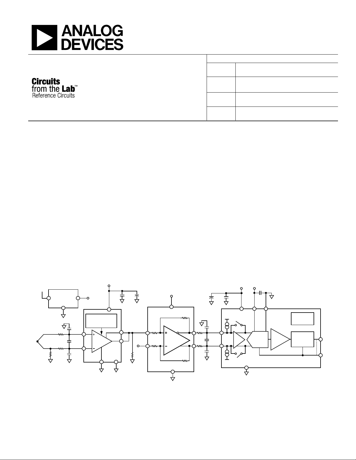
K-Type Thermocouple Measurement System with Integrated Cold Junction
Compensation
EVALUATION AND DESIGN SUPPORT
Circuit Evaluation Boards
CN-0271 Circuit Evaluation Board (EVAL-CN0271-SDPZ)
System Demonstration Platform, SDP-B (EVAL-SDP-CB1Z)
Design and Integration Files
Schematics, Layout Files, Bill of Materials
CIRCUIT FUNCTION AND BENEFITS
The circuit shown in Figure 1 is a complete thermocouple signal
conditioning circuit with cold junction compensation followed
by a 16-bit sigma-delta (Σ-Δ) analog-to-digital converter (ADC).
The AD8495 thermocouple amplifier provides a simple, low cost
solution for measuring K type thermocouple temperatures,
including cold junction compensation.
CN-0271
Devices Connected/Referenced
AD8495
AD8476
AD7790
ADR441
A fixed gain instrumentation amplifier in the AD8495 amplifies
the small thermocouple voltage to provide a 5 mV/°C output. The
high common-mode rejection of the amplifier blocks commonmode noise that the long thermocouple leads can pick up. For
additional protection, the high impedance inputs of the amplifier
make it easy to add extra filtering.
The AD8476 differential amplifier provides the correct signal levels
and common-mode voltage to drive the AD7790 16-bit, Σ-Δ ADC.
The circuit provides a compact low cost solution for thermocouple
signal conditioning and high resolution analog-to-digital
conversion.
Full K-Type Range 0°C to 50°C Thermocouple
Amplifier with Cold Junction Compensation
Low Power, Unity-Gain Fully Differential
Amplifier and ADC Driver
Reference with Current Sink and Source
Figure 1. K-Type Thermocouple Measurement System with Integrated Cold Junction Compensation (Simplified Schematic: All Connections Not Shown)
each circuit, and
suitability and applicability for your use and application. Accordingly, in no event shall Analog Devices
One Technology Way, P.O. Box 9106, Norwood, MA 02062-9106, U.S.A.
Tel: 781.329.4700
www.analog.com
Page 2
)2log(
57.16.6
log
××××
=
BandwidthGainDensityNoiseVoltage
V
BitsFreeNoise
MAX
OUT
bits12.4
log(2)
Hz8001.57122.4)HznV/(326.6
V4.9
log
=
××××
=
–2.0
–1.5
–1.0
–0.5
0
0.5
1.0
1.5
2.0
–50
0
50
100
150
200
250
300
350
400
450
500
550
600
650
700
750
800
850
900
950
ERROR (°C)
JUNCTION T E M P E R ATURE (° C)
AD8495
CN-0271
CN-0271 WITH
NONLINEARITY CORRECTION
10598-002
CN-0271 Circuit Note
CIRCUIT DESCRIPTION
The thermocouple is a simple, widely used component for
measuring temperature. It consists of a junction of two dissimilar
metals. These metals are connected at one end to form the
measurement junction, also called the hot junction. The other
end of the thermocouple is connected to the metal lines that
lead to the measurement electronics. This connection forms a
second junction: the reference junction, also called the cold
junction. To derive the temperature at the measurement junction
(T
MJ), the user must know the differential voltage created by
the thermocouple. The user must also know the error voltage
generated by the temperature at the reference junction (T
RJ).
The AD8476 is a very low power, fully differential precision
amplifier with integrated thin film, laser trimmed 10 kΩ gain
resistors for unity gain. It is an ideal choice for this application
because it presents a relatively high impedance load to the AD8495.
The AD7790 is a low power, complete analog front end for low
frequency measurement applications. It contains a low noise,
16-bit, Σ-Δ ADC with one differential input that can be buffered or
unbuffered.
Compensating for the reference junction error voltage is called
cold junction compensation. The electronics must compensate
for any changes in temperature at the reference (cold) junction
so that the output voltage is an accurate representation of the
hot junction measurement.
The circuit uses the AD8495 thermocouple amplifier on a single
5 V supply. The output voltage of the AD8495 is calibrated for
5 mV/°C. On a single 5 V supply, the output is linear between
approximately 75 mV and 4.75 V, corresponding to a temperature
range of 15°C to 950°C. The output of the AD8495 drives the
noninverting input of the AD8476 unity-gain differential amplifier,
which converts the single-ended input to differential outputs for
driving the AD7790 16-bit, Σ-Δ ADC.
A low-pass differential and common-mode filter before the
input of the AD8495 prevents RF signals, which, if allowed to
reach the AD8495, can be rectified and appear as temperature
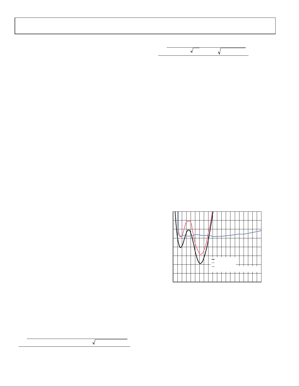
Test Results
An important measure of the performance of the circuit is the
amount of linearity error. The AD8495 output is accurate to
within 2°C from −25°C to +400°C. To achieve even greater
accuracy when operating at or outside of this range, a linearity
correction algorithm must be implemented in software. The
CN-0271 evaluation software uses NIST thermoelectric voltage
lookup tables to achieve an output error within 1°C from 15°C
to 950°C.
Figure 2 compares the performance of the AD8495 with the
CN-0271 system, and the result of applying the linearization
correction to the ADC output. For details on how the algorithm
was implemented in the software, see the AN-1087 Application
Note, Thermocouple Linearization When Using the AD8494/
AD8495/AD8496/AD8497.
fluctuations. The two 100 Ω resistors and the 1 µF capacitor
form a differential filter with a cutoff frequency of 800 Hz. The
two 0.01 µF capacitors form common-mode filters with a cutoff
frequency of 160 kHz. A similar filter is used at the output of
the AD8476 differential amplifier before the signal is applied
to the AD7790 ADC.
The AD8495 inputs are protected from input voltage excursions
up to 25 V from the opposite supply rail. For example, in this
circuit, with a 5 V positive supply rail and the negative supply
rail tied to GND, the part can safely withstand voltages at the
inputs from −20 V to +25 V. Voltages at the reference and sense
pins should not go beyond 0.3 V of the supply rails. This feature
is of particular importance in applications with power supply
sequencing issues that can cause the signal source to be active
before the supplies to the amplifier are applied.
The theoretical resolution of the system can be calculated from
the bandwidth, voltage noise density, and gain of the AD8495.
The peak-to-peak (noise free code) resolution in bits is
Rev. A | Page 2 of 5
Figure 2. Output Error of AD8495, Total CN-0271 Circuit Error, and
Total CN-0271 Circuit Error with Thermocouple Nonlinearity Correction
Page 3

Circuit Note CN-0271
bits13.4
log(2)
pVp100.449
V4.9
log
log(2)
log
3
=
−×
=
=
−
−pVp
IN
Noise
V
BitsFreeNoise
MAX
0
50
100
150
200
250
300
350
400
450
500
4CC4 4CC5 4CC6 4CC7 4CC8 4CC9
NUMBER OF O CCURANCE S
ADC CODE IN HEX
10598-003
The noise performance of the system is also important to the
accuracy of the circuit. Figure 3 shows a histogram of 1,000
measurement samples. This data was taken with the CN-0271
evaluation board connected to the EVA L-SDP-CB1Z System
Demonstration Platform (SDP-B) evaluation board. Details
of the setup are described in the Circuit Evaluation and Test
section.
The measured peak-to-peak noise is approximately 6 LSBs
(1 LSB = 4.9 V ÷ 65536 = 74.8 µV), corresponding to
0.449 mV p-p and 13.4 bits of noise free resolution.
This shows that the converter does not decrease the noise
free resolution because the measured resolution of a fixed
thermocouple input voltage results in approximately the same
number of noise free bits as predicted by the theoretical output
noise of the AD8495.
COMMON VARIATIONS
To measure negative temperatures, apply a voltage at the
reference pin to offset the output voltage at 0°C. The output
voltage of the AD8495 is
V
= (TMJ × 5 mV/°C) + V
OUT
REF
The complete K type thermocouple range of −200°C to +1250°C
can be measured by modifying the circuit to run on dual supplies.
When operating the AD8495 on a single supply, measurement
of temperatures less than ambient become nonlinear because
the output starts to saturate close to the supply rail. To maintain
accuracy at lower temperatures, use dual supplies or level-shift
the output by applying the appropriate offset voltage to the
reference pin.
The AD8494 is calibrated for J type thermocouples. Both the
AD8494 and AD8495 are optimized for reference junctions
between 0°C and 50°C.
The AD8496 (J type) and AD8497 (K type) are optimized for
reference junctions between 25°C and 100°C.
The circuit is proven to work with good stability and accuracy.
CIRCUIT EVALUATION AND TEST
This circuit uses the EVA L -CN0271-SDPZ circuit board and
the System Demonstration Platform (SDP-B) controller board
(EVA L -SDP-CB1Z). The two boards have 120-pin mating
connectors, allowing for the quick setup and evaluation of the
performance of the circuit. The E VAL-CN0271-SDPZ contains
the circuit to be evaluated, as described in this note, and the
SDP-B controller board is used with the CN-0271 evaluation
software to capture the data from the EVA L-CN0271-SDPZ
circuit board.
Equipment Needed
The following equipment is needed:
Figure 3. Histogram of Codes for 1,000 Samples at 120 Hz
A complete design support package for this circuit note can be
found at www.analog.com/CN0271-DesignSupport.
• A PC with a USB port and Windows® XP or Windows
Vista® (32-bit), or Windows® 7 (32-bit)
• The E VA L-CN0271-SDPZ circuit evaluation board
• The SDP-B controller board (E VAL -SDP-CB1Z) or the
SDP-S controller board (EVA L-SDP-CS1Z)
• The CN-0271 SDP evaluation software
• The 6 V power supply (EVA L -CFTL-6V-PWRZ) or
equivalent dc power supply
Getting Started
Load the evaluation software by placing the CN-0271 evaluation
software CD in the CD drive of the PC. Using My Computer,
locate the drive that contains the evaluation software.
Functional Block Diagram
See Figure 1 of this circuit note for the circuit block diagram and
the E VA L-CN0271-SDPZ-SCH-RevA.pdf file for the circuit
schematics. This file is contained in the CN-0271 Design
Support Package.
Rev. A | Page 3 of 5
Page 4

CN-0271 Circuit Note
10598-004
10598-005
USB CABLE
EVAL-CN0271-SDPZ BOARD
K-TYPE
THERMOCOUPLE
CONNECTOR
EVAL-CFTL-6V-PWRZ
POWER CO NNE C TOR
EVAL-SDP-CB1Z BOARD
Setup
Connect the 120-pin connector on the E VAL -CN0271-SDPZ
circuit board to the CON A connector on the SDP-B controller
board (E VA L-SDP-CB1Z). Use nylon hardware to firmly secure the
two boards, using the holes provided at the ends of the 120-pin
connectors.
With power to the supply off, connect the E VA L-CFTL-6V-PWRZ
plug to the barrel connector designated by J5 on the board. If this is
unavailable, connect the +6V and GND pins to the provided two
pin screw of J4 on the board. Also, connect the USB cable supplied
with the SDP-B board to the USB port on the PC.
Then, connect a K type thermocouple connector to J1 on the
board and the other end to the test equipment.
Test
Launch the evaluation software and connect the USB cable from
the PC to the mini-USB connector on the SDP-B board. Once USB
communications are established, the SDP-B board can now be used
to send, receive, and capture serial data from the EVA L -CN0271-
SDPZ board.
Figure 4 shows a screenshot of the CN-0271 SDP-B evaluation
software interface, and Figure 5 shows a photo of the E VA L-
CN0271-SDPZ evaluation board and the SDP-B board.
Information regarding the SDP-B board can be found in
the UG-277 user guide.
Figure 4. CN-0271 SDP-B Evaluation Software Interface
Figure 5. EVAL-CN0271-SDPZ Evaluation Board Connected to the SDP-B Board
Rev. A | Page 4 of 5
Page 5

Circuit Note CN-0271
(Continued from first page) Circuits from the Lab circuits are intended only for use with Analog Devices products and are the intellectual property of Analog Devices or its licensors. While you
reserves the right to change any Circuits from the Lab circuits at any time without notic e but is under no obligation to do so.
registered trademarks are the property of their respective owners.
LEARN MORE
CN0271 Design Support Package:
www.analog.com/CN0271-DesignSupport
SDP-B User Guide
Ardizzoni, John. A Practical Guide to High-Speed Printed-
Circuit-Board Layout, Analog Dialogue 39-09, September
2005.
Duff, Matthew and Towey, Joseph. Two Ways to Measure
Temperature Using Thermocouples Feature Simplicity,
Accuracy, and Flexibility. Analog Dialog 44-10, October
2010.
Malik, Reem. Thermocouple Linearization When Using the
AD8495/AD8496/AD8497, Application Note AN-1087,
Analog Devices.
MT-031 Tutorial, Grounding Data Converters and Solving the
Mystery of “AGND” and “D GND”, Analog Devices.
MT-035, Op Amp Inputs, Outputs, Single-Supply, and Rail-to-
Rail Issues, Analog Devices.
MT-036 Tutorial, Op Amp Output Phase-Reversal and Input
Over-Voltage Protection, Analog Devices.
MT-068 Tutorial, Difference and Current Sense Amplifiers,
Analog Devices.
MT-101 Tutorial, Decoupling Techniques, Analog Devices.
Data Sheets and Evaluation Boards
CN-0271 Circuit Evaluation Board (EVAL-CN0271-SDPZ)
System Demonstration Platform, SDP-B (E VA L-SDP-CB1Z)
AD8495 Data Sheet
AD8476 Data Sheet
AD7790 Data Sheet
ADR44x Data Sheet
ADP3336 Data Sheet
REVISION HISTORY
6/12—Rev. 0 to Rev. A
Changes to Figure 1 .......................................................................... 1
6/12—Revision 0: Initial Version
may use the Circuits from the Lab circuits in the design of your product, no other license is granted by implication or otherwise under any patents or other intellectual property by
application or use of the Circuits from the Lab circuits. Information furnished by Analog Devices is believed to be accurate and reliable. However, Circuits from the Lab circuits are supplied
"as is" and without warranties of any kind, express, implied, or statutory including, but not limited to, any implied warranty of merchantability, noninfringement or fitness for a particular
purpose and no responsibility is assumed by Analog Devices for their use, nor for any infringements of patents or other rights of third parties that may result from their use. Analog Devices
©2012 Analog Devices, Inc. All rights reserved. Trademarks and
CN10598-0-6/12(A)
Rev. A | Page 5 of 5
 Loading...