

Page 1

Circuit Note
Differential SD Video Filter Amplifier with
Rev. 0
Circuits from the Lab™ circuits from Analog Devices have been designed and built by Analog Devices
Standard engineering practices have been employed in the design and construction of
each circuit, and their function and performance have been tested and verified in a lab environment at
suitability and applicability for your use and application. Accordingly, in no event shall Analog Devices
be liable for direct, indirect, special, incidental, consequential or punitive damages due to any cause
whatsoever connected to the use of any Circuits from the Lab circuits. (Continued on last page)
Fax: 781.461.3113 ©2012 Analog Devices, Inc. All rights reserved.
Circuits from the Lab™ reference circuits are engineered and
tested for quick and easy system integration to help solve today’s
analog, mixed-signal, and RF design challenges. For more
information and/or support, visit www.analog.com/CN0264.
Devices Connected/Referenced
ADV7391/
ADV7393
ADA4432-1
ADA4433-1
Low Power, Chip Scale 16-/8-Bit SD/HD
Video Encoder
Single-Ended SD Video Filter Amplifier
with Output Short-to-Battery Protection
Output Short-to-Battery Protection
CN-0264
A Robust Solution for Transmitting Composite Video with Output Short-to-Battery
Protection
EVALUATION AND DESIGN SUPPORT
Circuit Evaluation Boards
CN-0264 Circuit Evaluation Board (EVAL-CN0264-EB1Z)
Design and Integration Files
Schematics, Layout Files, Bill of Materials
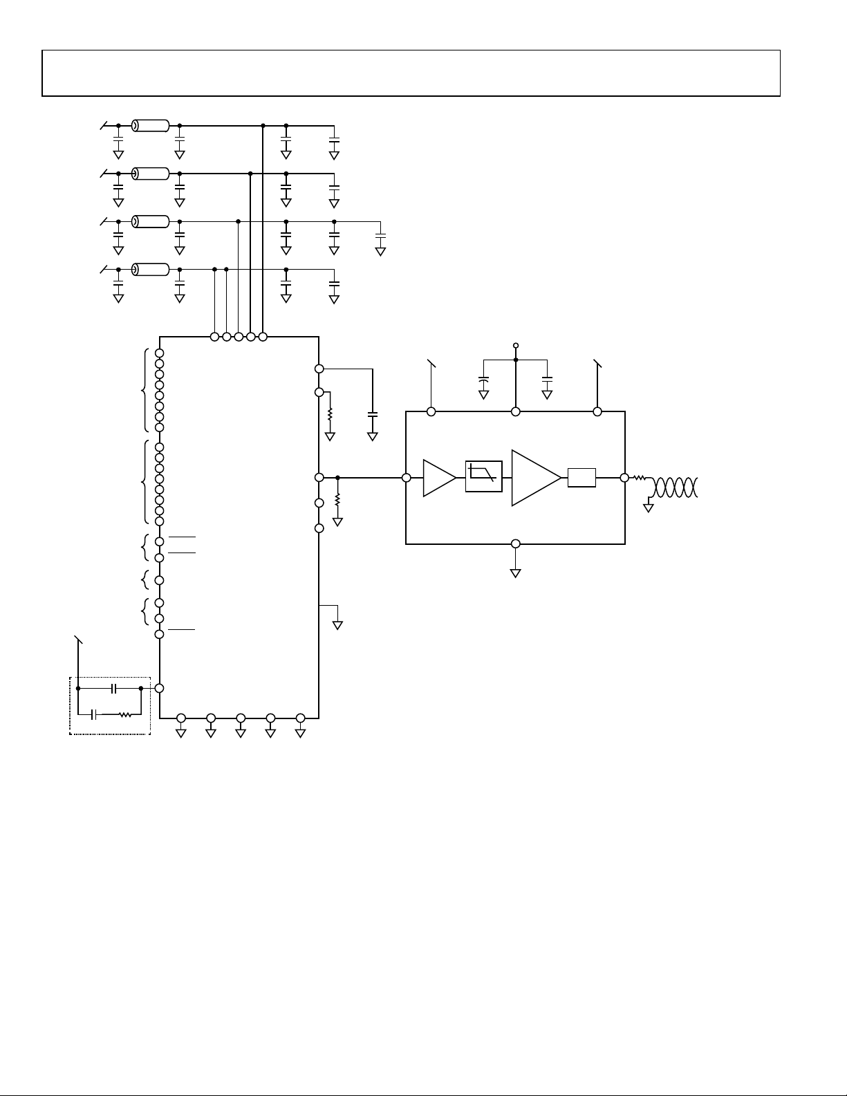
CIRCUIT FUNCTION AND BENEFITS
The circuit in Figure 1 shows a digital-to-analog video converter
paired with a low cost, low power, fully integrated reconstruction
video filter with output short-to-batter y (STB) protection, ideal for
CVBS video transmission in harsh infotainment environments
such as automotive applications. Although many video encoders
(video DACs), such as the ADV7391, can drive a video load
directly, it is often beneficial to use a video driver at the output
of a video encoder for power savings, filtering, line driving, and
overvoltage circuit protection. The main purpose of a video
driver, typically configured as an active filter (also known as a
reconstruction filter), is twofold: it blocks the higher frequency
components (above the Nyquist frequency) that were introduced
into the video signal as part of the sampling process, and it provides
gain to drive the external
Designers of infotainment and other video systems, such as
rearview cameras and rear-seat entertainment systems, are likely
to use this circuit to transmit video for the reasons previously
stated. However, a third pressing design issue centers on the
robustness. The ADA4432-1 and ADA4433-1 provide analog
video designers with integrated ICs that offer crucial overvoltage
protection, hardened ESD tolerance, along with excellent video
specification, low power consumption, and wire diagnostic
features.
75 Ω cable to the video display.
The ADA4432-1 and ADA4433-1 are fully integrated, single-ended
and differential video reconstruction filters, respectively. They
combine overvoltage protection (STB protection) up to 18 V on
the outputs, with low power consumption and a wire diagnostic
capability. Wire diagnostics are provided by way of a logic output
that is activated when a fault condition is present. The ADA4432-1
and ADA4433-1 feature a high-order filter with a −3 dB cutoff
frequency of 10 MHz and 45 dB of rejection at 27 MHz.
The combination of STB protection and robust ESD tolerance
allows the ADA4432-1 and ADA4433-1 to provide superior
protection in the hostile environments.
The ADV7391 and ADA4432-1 are fully automotive qualified,
which makes both products ideal for infotainment and visionbased safety systems for automotive applications. The ADV7391,
ADA4432-1, and the ADA4433-1 are available in a very small
LFCSP package ideal for small footprint applications.
CIRCUIT DESCRIPTION
The ADV7391 is a low power, fully integrated digital video encoder
that converts digital 8-bit component video data from a CMOS
imager into a standard analog baseband video signal compatible
with worldwide standards. Three, 10-bit digital-to-analog video
converters (operating on V
for composite (CVBS), S-video (YC), or component (YPrPb/RGB)
analog outputs in either standard definition (SD) or high definition
(HD) video formats. The circuit in Figure 1 is configured for low
output drive through DAC1 only. To conserve more power, the
other DACs and phase-locked loop (PLL) are turned off. Low drive
mode is defined as 4.33 mA full-scale output current. The
ADV7391 contains an R
R
pin and AGND is used to control the full-scale output current.
SET
For low drive operation, R
equal 300 Ω. The resistor connected to the R
1% tolerance.
= 2.6 V to 3.46 V) provide support
AA
pin. A resistor connected between the
SET
must equal 4.12 kΩ, and RL must
SET
pin must have a
SET
engineers.
room temperature. However, you are solely responsible for testing the cir cuit and determinin g its
One Technology Way, P.O. Box 9106, Norwood, MA 02062-9106, U.S.A.
Tel: 781.329.4700
www.analog.com
Page 2
CN-0264 Circuit Note
P0
P1
P2
P3
P4
P5
P6
P7
DGNDPGND
DGNDPGND
0.1µF
GND_IO
100nF
GND_IO
33µF
GND_IO
10µF
GND_IO
FERRITE BE AD
V
DD_IO
0.1µF
PGND
100nF
PGND
33µF
PGND
10µF
PGND
PV
DD
0.1µF
AGND
100nF
AGND
33µF
AGND
10µF
AGND
V
AA
0.1µF
DGND
100nF
DGND
33µF 10µF
DGND
V
DD
V
DD_IO
PV
DD
V
AA
V
DD
ADV7391/AD7393
HSYNC
VSYNC
CLKIN
AGND
AGND
DGND
DGND
GND_IO
GND_IO
R
SET
AGND
DAC 1
DAC 2
DAC 3
AGND
300Ω
COMP
2.2nF
EXT_LF
SDA
SCL
ALSB
RESET
PIXEL PORT
INPUTS
CONTROL
INPUTS/OUTPUTS
CLOCK INPUT
I
2
C PORT
DGND
V
DD
EXTERNAL LOOP
FILTER
(OPTIONAL)
1µF
AGND
4.12kΩ
75Ω
TWISTED
PAIR
PV
DD
150nF 170Ω
12nF
DGND
P8
P9
P10
P11
P12
P13
P14
P15
PIXEL PORT
INPUTS
(ADV7393 ONLY)
IN
GND
ENA
+V
S
OUT
0.1µF2.2µF
ENABLE
(INPUT)
STB
75Ω
V
AA
LFCSP PACKAGE
ADA4432-1
STB
(OUTPUT)
STB
V
AA
= 3.3V
V
DD
= 1.8V
PV
DD
= 1.8V
V
DD_IO
= 1.8V, 2.5V, OR 3.3V
LPF
10488-001
The ADV7391 includes an on-chip, PLL that allows for oversampling video data. As shown in Figure 1, the PLL is disabled
(Subaddress 0x00, Bit 1 = 1) providing an SD oversample rate of
2×. With the PLL disabled, the external loop filter components
are removed to save space and cost.
The ADA4432-1 can be used as a pseudo differential (single-
ended) driver with an unbalanced transmission line. The pseudo
differential mode uses a single conductor to carry an unbalanced
data signal from the driver to the receiver, while a second
conductor is used as a ground reference signal.
Figure 1. Low Cost, Fully Integrated Reconstruction Filter using the ADA4432-1 (All Connections and Decoupling Not Shown)
The positive conductor connects the ADA4432-1 output to the
positive input of a differential receiver. The negative wire or ground
conductor from the source circuitry connects to the negative input
of the receiver. The output termination of the ADA4432-1 should
match the impedance of the input termination at the receiver.
For example, in a 75 Ω system, each output of the ADA4432-1 is
back terminated with 75 Ω resistors that are connected to a
resistance of 75 Ω at the receiver.
Rev. 0 | Page 2 of 5
In Figure 1, the ADA4432-1 is configured as a single-ended-tosingle-ended driver that allows unbalanced transmission using
twisted pair cable, untwisted cable, or coaxial cable.
Page 3

Circuit Note CN-0264
75Ω CABLE
75Ω
75Ω
510Ω
3.3V
ADV7391
R
SET
10488-002
75Ω CABLE
300Ω
4.12kΩ
3.3V
3.3V
75Ω
75Ω
ADV7391
R
SET
10488-003
ADA4432-1
0
–10
–20
–30
–40
–50
–60
–70
–80
–90
–100
4 104 204 304
FREQUENCY (MHz)
LOG MAGNITUDE (dB)
404 504
10488-004
0
–10
–20
–30
–40
–50
–60
–70
–80
–90
–100
4 104 204 304
FREQUENCY (MHz)
LOG MAGNITUDE (dB)
404 504
10488-005
Low Power Considerations
Using a series source termination and a shunt load termination
on a low supply voltage with the ADA4432-1 or the ADA4433-1
realizes significant power savings compared to driving a video
cable directly from a DAC output. Figure 2 shows a video DAC
driving a cable directly. Properly terminated, a DAC driven
transmission line requires two 75 Ω loads in parallel, demanding
in excess of 33 mA to reach a full-scale voltage level of 1.3 V.
Figure 3 shows the same video load being driven using the
ADA4432-1 and a series-shunt termination. This requires two
times the output voltage to drive the equivalent of 150 Ω but
only requires a little more than 15 mA to reach a full-scale output.
When running on the same supply voltage as the DAC, this
results in a 74% reduction in power consumption compared to
the circuit in Figure 2. The high-order filtering provided by the
ADA4432-1 lowers the requirements on the DAC oversampling
ratio, thereby realizing further power savings. The main source
for power savings realized by the configuration shown in Figure 3
comes from the low drive mode setting for the ADV7391. This
along with the reduction in the requirement for oversampling
(PLL turned off ) and the reduced load current required results
in significant power savings.
For more information on low drive mode, refer to the ADV7391
data sheet.
In addition, image frequency sidebands can create radiation
emissions in the output traces and cabling that are potentially
disruptive to adjacent circuitry and other electronic systems. To
reduce the effect of radiation emissions, remove all unwanted high
frequency components before transmitting along the printed circuit
board (PCB) traces and transmission cables. The ADA4432-1
helps reduce EMI by filtering the DAC output and removing
unwanted high frequency content. Figure 4 to Figure 6 illustrate
this point.
Figure 4 shows the frequency spectrum of a CVBS video signal
at the output of the ADV7391 without the ADA4432-1. The
spectrum shows a signal whose content bandwidth is 6.5 MHz,
with sidebands at 27 MHz, 54 MHz, 108 MHz, and so on. The
ADV7391 is operating in full output drive mode with the PLL
turned off at 2× oversampling.
Figure 2. Driving a Video Transmission Line Directly with a DAC
Figure 3. Driving a Video Transmission Line with the ADA4432-1
EMI and EMC Considerations
The analog output of video DACs like the ADV7391 requires
low-pass filtering to remove unwanted signal components at
frequencies more than the sample rate or frequency sidebands.
The conversion of a digital-to-analog signal creates duplicated
images in the frequency domain, at multiples of the sampling
frequency. Removing these frequency sideband components is
the main function of the reconstruction filters. These filters
significantly attenuate the sideband signals, preventing aliasing
when the DAC outputs are decoded. Aliasing error can create
image quality issues.
Figure 4. CVBS Measured Directly at the Output of the ADV7391, PLL Off,
2× Oversampling, Full Output Drive Mode
Figure 5 show the frequency spectrum of the same CVBS signal
at the output of the ADV7391 without the ADA4332-1. The
difference here is that the ADV7391 is operating in full output
drive mode with the PLL turned on at 8× oversampling.
Figure 5. CVBS Measured Directly at the Output of the ADV7391, PLL On,
8× Oversampling, Full Output Drive Mode
Rev. 0 | Page 3 of 5
Page 4

CN-0264 Circuit Note
0
–10
–20
–30
–40
–50
–60
–70
–80
–90
–100
4 104 204 304
FREQUENCY (MHz)
LOG MAGNITUDE (dB)
404 504
10488-006
–IN
AGND
AGND
AGND AGND
GND
AGND
ENA
ADV7391
DAC 1
+V
S
V
S
+OUT
0.1µF2.2µF
0.1µF
ENABLE
(INPUT)
STB
37.5Ω
1.33kΩ
7.5kΩ
300Ω
37.5Ω
V
S
ADA4433-1
STB FLAG
(OUTPUT)
STB
LPF
+IN
–OUT
STB
LPF
75Ω
TWISTED
PAIR
10488-007
Figure 6 shows the frequency spectrum of the same CVBS signal
with the ADA4432-1 filtering the output of the ADV7391. All
sidebands are attenuated to less than 50 dB. The ADV7391 is
operating in low output drive mode with the PLL turned off at
2× oversampling.
Figure 6. CVBS Measured at the Output of the ADA4432-1, PLL Off,
2× Oversampling, Low Output Drive Mode
PCB Layout Considerations
In any circuit where accuracy is crucial, it is important to consider
the power supply and ground return layout on the board. Isolate
the digital and analog sections of the PCB as much as possible.
This PCB was constructed in a 4-layer stack up with large area
ground plane layers and power plane polygons. See the MT-031
Tuto r ia l for more discussion on layout and grounding and the
MT-101 Tut o ri a l for information on decoupling techniques.
Decouple the power supply to the ADV7391 with 10 µF and 0.1 µF
capacitors. Decouple the ADA4432-1 and the ADA4433-1 output
amplifiers with 0.1 µF and 22 µF capacitors to properly suppress
noise and reduce ripple. Place the capacitors as close to the device
as possible with the 0.1 µF capacitor having a low ESR value.
Ceramic capacitors are advised for all high frequency decoupling.
It is important to keep the two ICs as close to each other as possible.
Power supply lines should have as large a trace width as possible
to provide low impedance paths and reduce glitch effects on the
supply line. Shield clocks and other fast switching digital signals
from other parts of the board by digital ground.
A complete design support package for this circuit note, including
the board layouts, can be found at
http://www.analog.com/CN0264-DesignSupport.
COMMON VARIATIONS
Many applications require differential output instead of singleended output. For these applications, the ADA4432-1 is replaced
with the ADA4433-1.
The ADA4433-1 is a fully differential filter/driver that can be used
as a single-ended-to-differential amplifier or as a differential-todifferential amplifier. In Figure 7, the ADA4433-1 is configured
as a single-ended-to-differential output driver. In single-endedto-differential output applications, bias the INN input appropriately
to optimize the output range. To make the most efficient use of
the output range of the ADA4433-1, especially with low supply
voltages, it is important to allow the differential output voltage
to swing in both a positive and negative direction around the
output common-mode voltage (V
point (1.65 V).
To do this, the −IN input is biased at the midpoint of the expected
input signal range, as shown in Figure 7. This is done with a voltage
divider to the supply voltage (7.5 kΩ and 1.33 kΩ connected
between the 3.3 V supply and GND biases −IN to 0.5 V). The
0.1 µF capacitor helps to filter high frequency supply noise. A
1 V p-p single-ended signal on +IN, with −IN biased at 0.5 V
produces a differential input voltage of −0.5 V to +0.5 V. The
resulting differential output swings above and below the V
level (1.65 V). The ADA4433-1 o
1.15 V to 2.15 V, requiring only 1 V of the output range to
produce a 1 V p-p signal at the receiver.
) level; the midsupply
OCM
OCM
utput voltage now extends from
Figure 7. ADA4433-1 Typical Application Circuit
Rev. 0 | Page 4 of 5
Page 5

Circuit Note CN-0264
(Continued from first page) Circuits from the L ab circuits are intended only for use with Analog Devices products and are the intellectual property of Analog Devices or its licensors. While you
reserves the right to change any Circuits from the Lab circuits at any time without notice but is under no obligation to do so.
registered trademarks are the property of their respective owners.
The differential outputs of the ADA4433-1 allow fully balanced
transmission using twisted or untwisted pair cable. In this
configuration, the differential output termination consists of one
source resistor on each output. Both resistors are equal to half
the receiver input termination. For example, in a 75 Ω system,
each output of the ADA4433-1 is back terminated with 37.5 Ω
resistors connected to a differential resistance of 75 Ω at the
receiver.
CIRCUIT EVALUATION AND TEST
This circuit uses the E VA L-CN0264-EB1Z circuit board, which
contains the circuit to be evaluated, as described in this note.
The Cypress USB microcontroller is used to configure and load
software to and from the EVA L-CN0264-EB1Z board.
Equipment Needed
The following equipment is needed:
• A PC with a USB port and Windows® XP or Windows Vista®
(32-bit), or Windows® 7 (32-bit)
• The E VA L-CN0264-EB1Z circuit evaluation board
• The CN-0264 evaluation software
• A power supply: 7.5 V wall wart
• A Spectrum Analyzer: Agilent E4440A, or equivalent
Getting Started
Load the evaluation software by placing the CN0264 evaluation
CD in the CD drive of the PC. Using My Computer, locate the
drive that contains the evaluation software CD and open the
Readme file. Follow the instructions contained in the Readme
file for installing and using the evaluation software.
Functional Block Diagram
See Figure 1 of this circuit note for the circuit block diagram
and the E VAL -CN0264-EB1Z-SCH.pdf file for the circuit
schematics. This file is contained in the CN0264 Design
Support Package.
Setup
With power to the supply off, connect a 7.5 V power supply to
the 7.5 V terminal and the GND terminal on the board. If
available, a 7.5 V wall wart can be connected to the barrel
connector on the board and used in place of the 7.5 V power
supply. Connect the USB cable to the USB port on the PC. Do
not connect the USB cable to the mini-USB connector on the
board at this time.
Test
Apply power to the 7.5 V supply (or wall wart) connected to the
EVA L-CN0264-EB1Z circuit board. Launch the evaluation
software and connect the USB cable from the PC to the miniUSB connector on the PCB.
Information and details regarding how to use the evaluation
software for data capture can be found in the CN-0264 evaluation
software Readme file.
LEARN MORE
CN0264 Design Support Package:
http://www.analog.com/CN0264-DesignSupport
AN-617, Wafer Level Chip Scale Package, Analog Devices.
MT-031 T
utorial, Grounding Data Converters and Solving the
Mystery of "AGND" and "DGND," Analog Devices.
MT-101 Tutorial, Decoupling Techniques, Analog Devices.
Data Sheets and Evaluation Boards
CN-0264 Circuit Evaluation Board (EVAL-CN0264-EB1Z)
ADV7391 Data Sheet
ADV7391 Evaluation Board
ADA4432-1 Data Sheet
ADA4432-1 Evaluation Board
ADA4433-1 Data Sheet
ADA4433-1 Evaluation Board
REVISION HISTORY
6/12—Revision 0: Initial Version
may use the Circuits from the Lab circuits in the design of your product, no other license is granted by implication or otherwise under any patents or other intellectual property by
application or use of the Circuits from the Lab circuits. Information furnished by Analog Devices is believed to be accurate and reliable. However, Circuits from the Lab circuits are supplied
"as is" and without warranties of any kind, express, implied, or statutory including, but not limited to, any implied warranty of merchantability, noninfringement or fitness for a particular
purpose and no responsibility is assumed by Analog Devices for their use, nor for any infringements of patents or other rights of third parties that may result from their use. Analog Devices
©2012 Analog Devices, Inc. All rights reserved. Trademarks and
CN10488-0-6/12(0)
Rev. 0 | Page 5 of 5
 Loading...