

Page 1
Circuit Note
CN-0261
Ultralow Distortion, Ultralow Noise
Amplifier
ADR435
Ultralow Noise XFET 5 V Reference
Rev.0
Circuits from the Lab™ circuits from Analog Devices have been designed and built by Analog Devices
have been employed in the design and construction of
each circuit, and their function and performance have been tested and verified in a lab environment at
room temperature. However, you are solely responsible for testing the circuit and determining its
uitability and applicability for your use and application. Accordingly, in no event shall Analog Devices
be liable for direct, indirect, special, incidental, consequential or punitive damages due to any cause
whatsoever connected to the use of any Circuits from the Lab circuits. (Continued on last page)
Fax: 781.461.3113 ©2012 Analog Devices, Inc. All rights reserved.
VIN+
VIN–
IN+
IN–
ADR435
5V VREF
VDD = 5V
3-WIRE INTERFACE
SCK
SDO
CNV
VIO
SDI
REF
49.9Ω
VDD
AD8597
GND
9
8
5
10
6
7
2
3
1
4
6
3
2
7
1
3
2
7
1
49.9Ω
49.9Ω
180Ω
180Ω
2.7nF
2.7nF
VCM
0.1µF
590Ω
590Ω
VCM
0.1µF
590Ω
590Ω
1µF
0.1µF
VDD = 8V
VDD = 8V
6
2
4
VIN
GND
VOUT
0.1µF
VDD = 8V
0.1µF
VIO =
1.8V TO 5V
AD7691
AD8597
VSS = –2V
VSS = –2V
22µF
VCM = 2.5V
GND
VREF = 5V
VIN+
VIN–
VCM = VREF ÷ 2
= 2.5V
VCM = VREF ÷ 2
= 2.5V
VOLTAGE DIVIDER
FOR BIASI NG PURPOSES
VOLTAGE DIVIDER
FOR BIASI NG PURPOSES
18-BIT, 1.5LSB INL
250kSPS DIFF ERENTIAL
PulSAR ADC
0.1µF
0.1µF
0.1µF
0.1µF
49.9Ω
10467-001
Circuits from the Lab™ reference circuits are engineered and
tested for quick and easy system integration to help solve today’s
analog, mixed-signal, and RF design challenges. For more
information and/or support, visit www.analog.com/CN0261.
AD7691 18-Bit 1.5 LSB INL, 250 kSPS PulSAR ADC
AD8597
Optimizing AC Performance in an 18-bit, 250 kSPS, PulSAR Measurement Circuit
Devices Connected/Referenced
EVALUATION AND DESIGN SUPPORT
Circuit Evaluation Boards
CN-0261 Circuit Evaluation Board (EVAL-CN0261-SDPZ)
System Demonstration Platform (EVAL-SDP-CB1Z)
Design and Integration Files
Schematics, Layout Files, Bill of Materials
CIRCUIT FUNCTION AND BENEFITS
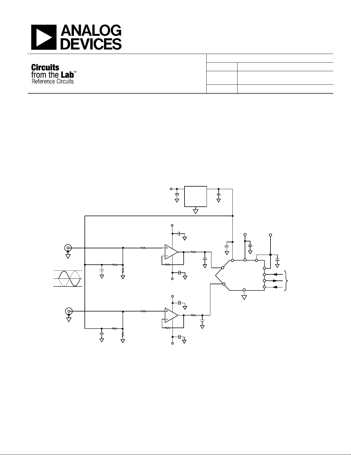
Choosing complementary products for high performance ADCs
can be a challenge. The circuit in Figure 1 shows a complete
front end solution for the 18-bit, 250 kSPS PulSAR® ADC,
which is optimized for ac performance.
engineers. Standard engineering practices
s
Figure 1. High Performance, 18-Bit ADC Front End (Simplified Schematic: All Connections and Decoupling Not Shown)
One Technology Way, P.O. Box 9106, Norwood, MA 02062-9106, U.S.A.
Tel: 781.329.4700
www.analog.com
Page 2
CN-0261 Circuit Note
10467-002
–250
–200
–150
–100
0
–50
0 20 40 60
FREQUENCY (kHz)
AMPLITUDE (dB)
80 100 120
10467-003
FUNDAMENTAL = 1kHz, –0.3dB
FROM FS
SAMPLING FREQUENCY = 250kSPS
SNR = 101.02dB
THD = –118.44dB
SINAD = 100.94dB
DYNAMIC RANGE = 101.5dB
The circuit centers on the AD7691, which is a low power ADC
(1.35 mW @ 2.5 V and 100 kSPS) from the PulSAR family.
The ADC is driven directly from the AD8597 ultralow
distortion, ultralow noise amplifier, and the ADC’s reference is
the ultralow noise 5 V ADR435. The circuit achieves 101 dB
SNR and 118 dB THD with a 1 kHz input tone.
CIRCUIT DESCRIPTION
The heart of this circuit is the AD7691, an 18-bit, 250 kSPS
charge redistribution, successive approximation, analog-todigital converter (ADC) that operates from a single power
supply.
It contains a low power, high speed, 18-bit sampling ADC with
no missing codes, an internal conversion clock, and a versatile
serial interface port. On the CNV rising edge, it samples the
voltage difference between the IN+ and IN− pins. The voltages
on these pins swing in opposite phases between 0 V and REF.
The reference voltage, REF, is applied externally and can be set
up to the supply voltage. The AD7691 power scales linearly with
throughput.
For the experiments carried out for this circuit note, the
AD7691was interfaced to the SDP (System Demonstration
Platform board, EVA L-SDP-CB1Z), and the ADC SPIcompatible serial interface was connected to the DSP SPORT
interface VIO supply.
The AD7691 is housed in a 10-lead MSOP or a 10-lead QFN
(LFCSP).
The ADC is driven from the AD8597 (4.8 mA/amplifier), which
is a low noise, low distortion operational amplifiers ideal for use
as an input buffer. The low noise of 1.1 nV/√Hz and low
harmonic distortion of less than −120 dB at audio frequencies
give the AD8597 the wide dynamic range necessary for
preamplifiers in audio, medical, and instrumentation
applications. The excellent slew rate of 14 V/μs and 10 MHz
gain bandwidth product make it highly suitable for medical
applications.
The AD8597 can be operated on supply voltages up to ±15 V. In
the circuit, supply voltages of +8 V and −2 V were chosen in
order to minimize power dissipation.
The AD8597 is available in 8-lead SOIC and LFCSP packages.
The 180 Ω resistors and the 2.7 nF capacitors form a single-pole
327 kHz low-pass filter to further reduce noise.
The voltage reference used in this application is the ADR435,
which is one of a family of XFET® voltage references featuring
low noise, high accuracy, and low temperature drift
performance. Using patented temperature drift curvature
correction and XFET (eXtra implanted junction FET)
technology, voltage change vs. temperature is minimized.
The ADR43x family can source up to 30 mA of output current
and sink up to 20 mA. It also has a trim terminal to adjust the
output voltage over a 0.5% range without compromising
performance.
The ADR435 is available in either an 8-lead MSOP or an 8-lead
narrow SOIC package.
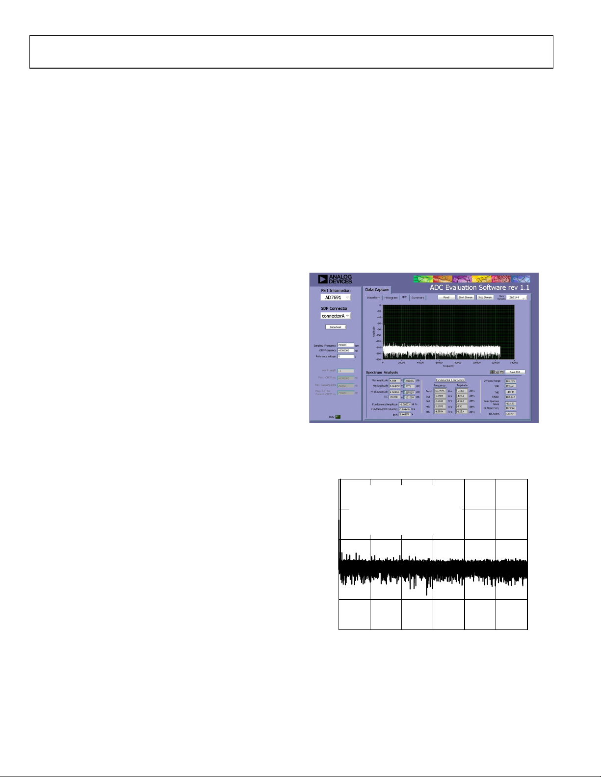
The dynamic performance of the above configuration is shown
in Figure 2 and Figure 3 and is summarized below:
SNR = 101.02dB
THD = 118.44 dB
SINAD = 100.94 dB
Dynamic Range = 101.5 dB
Figure 2. Evaluation Board Software Output Screen Capture
Figure 3. FFT Details for 1 kHz Tone Sampling at 250 kSPS
Rev. 0 | Page 2 of 4
Page 3

Circuit Note CN-0261
AUDIO
PRECISION
SYS-2522
DC
POWER SUPPLIES
EVAL-CN0261-SDPZ
SDP
BOARD
PC WITH
FFT
ANALYSIS
SOFTWARE
+8V +5V −2V
VIN+
VIN−
USB
120-PIN
CONNECTOR
GND
10nF
CERAMIC
10467-004
COMMON VARIATIONS
Other pin-compatible 18-bit ADCs in the PulSAR family are
available with higher sampling rates: AD7690 (400 kSPS),
AD7982 (1 MSPS), AD7984 (1.33 MSPS).
The AD7986 (2 MSPS) is available in 20-lead 4 mm × 4 mm
LFCSP (QFN).
The AD8599 op amp is a dual version of the AD8597 and can be
used in the circuit, if desired.
The ADA4841-1 (single) and ADA4841-2 (dual) are lower
power op amps (1.1 mA/amp), but have slightly higher noise
(2.1 nV/√Hz).
The ADA4941 is optimized for driving differential input 18-bit
ADCs and has 2.2 mA/amplifier and 10.2 nV/√Hz noise.
A summary of PulSAR ADCs and recommended drivers can be
found at www.analog.com/PulSAR.
Other reference voltages within the ADR43x family or from
other reference families are available from the Analog Devices
portfolio.
The inclusion of a buffer to create the VCM signal to bias the
input would be normal, however, specified performance was
achieved without the need of a buffer in this circuit.
CIRCUIT EVALUATION AND TEST
Equipment Needed (Equivalents Can Be Substituted)
• EVAL -CN0261-SDPZ circuit evaluation board
• System Demonstration Board (EVAL -SDP-CB1Z)
• Function generator, Audio Precision SYS-2522
• External 10 nF ceramic filter capacitor as shown in
Figure 4
• Power supplies: +8 V @ 50 mA, −2 V @ 50 mA, +5 V
@ 500 mA.
• PC with a USB port and Windows® XP or Windows
Vista® (32-bit), or Windows® 7 (32-bit)
Setup and Test
The block diagram of ac performance measurement setup
is shown in Figure 4. The EVAL-CN0261-SDPZ board is driven
with bench supplies as shown. Complete documentation for the
board can be found at www.analog.com/CN0261-DesignSupport.
To measure the frequency response, the equipment was
connected as shown in Figure 5. The Audio Precision SYS-2522
was set to output a 1 kHz tone at an input signal level of 0.5 dB
below full-scale. The external 10 nF capacitor acts as a low-pass
noise reduction filter for the output of the signal generator.
Using the evaluation board software, the FFT data was then
captured and analyzed.
The software analysis is part of the evaluation board software,
which allows the user to capture and analyze ac or dc
performance.
In addition to ac performance, the evaluation board software
also allows users to analyze the waveform data and create a
histogram for the measured input signal.
Figure 4. Test Setup for Measuring AC Performance
Rev. 0 | Page 3 of 4
Page 4

CN-0261 Circuit Note
(Continued from first page) Circuits from the L ab circuits are intended only for use with Analog Devices products and are the intellectual property of Analog Devices or its licensors. While you
reserves the right to change any Circuits from the Lab circuits at any time without notice but is under no obligation to do so.
red trademarks are the property of their respective owners.
LEARN MORE
CN0261Design Support Package:
www.analog.com/CN0261-DesignSupport
Ardizzoni, John. A Practical Guide to High-Speed Printed-
Circuit-Board Layout, Analog Dialogue 39-09, September
2005.
MT-021 Tutorial, Sucessive Approximation ADCs, Analog
Devices.
MT-031 Tutorial, Grounding Data Converters and Solving the
Mystery of "AGND" and "DGND," Analog Devices.
MT-101 Tutorial, Decoupling Techniques, Analog Devices.
Voltage Reference selection and Evaluation Tool, Analog
Devices.
Data Sheets and Evaluation Boards
CN-0261 Circuit Evaluation Board (EVAL-CN0261-SDPZ)
System Demonstration Platform (EVAL-SDP-CB1Z)
AD7691 Data Sheet
AD8597 Data Sheet
ADR435 Data Sheet
REVISION HISTORY
1/12—Revision 0: Initial Version
may use the Circuits fro m the Lab circuits in the design of your product, no other license is granted by implication or otherwise under any patents or other intellectual property by
application or use of the Circuits from the Lab circuits. Information furnished by Analog Devices is believed to be accurate and reliable. However, "Circuits from the Lab" are supplied "as is"
and without warranties of any kind, express, implied, or statutory including, but not limited to, any implied warranty of merchantability, noninfringement or fitness for a particular
purpose and no responsibility is assumed by Analog Devices for their use, nor for any infringements of patents or other rights of third parties that may result from their use. Analog Devices
©2012 Analog Devices, Inc. All rights reserved. Trademarks and
registe
CN10467-0-1/12(0)
Rev. 0 | Page 4 of 4
 Loading...