

Page 1
Circuit Note
CN-0251
Rev. 0
Circuits from the Lab™ circuits from Analog Devices have been designed and built by Analog Devices
each circuit, and their function and performance have been tested and verified in a lab environment at
room temperature. However, you are solely responsible for testing the circuit and determining its
nd application. Accordingly, in no event shall Analog Devices
be liable for direct, indirect, special, incidental, consequential or punitive damages due to any cause
whatsoever connected to the use of any Circuits from the Lab circuits. (Continued on last page)
Fax: 781.461.3113 ©2012 Analog Devices, Inc. All rights reserved.
D3V3
DGND
DGND AGND
–IN
IA
R
G
RG*
*OMIT R
G
FOR G = 1
R
G
+IN
+V
S
V
OUT
REF
–V
S
AD8226
ADP1720
–OUT
VN
VP
+OUT
NC
+IN 0.4x
–IN 0.8x
+IN 0.8x
–IN 0.4x
–V
S
+V
S
1kΩ
1.25kΩ
100Ω
100kΩ
100Ω
1.25kΩ
1kΩ
AD8475
1.25kΩ
1.25kΩ
MCLK1NCMCLK2
P0/REFIN2(–)
P1/REFIN2(+)
DVDDDGND
REFIN1(+)
REFIN1(–)
AIN2
AIN1
AIN3
AIN4
AINCOM
BPDSW
AGND
AD7192
TEMP
SENSOR
AV
DD
AGND
DOUT/RDY
DIN
SCLK
CS
SYNC
P3
P2
AV
DD
AGND
Σ-Δ
ADC
MUX
DOUT
DIN
SCLK
CS
SYNC
P3
P2
ADG1409
S1A
S4B
DA
1nF
IN OUT
GND
1nF
10nF
4.02kΩ
4.02kΩ
DB
S4A
S1B
VS1A
VS4B
VS4A
VS1B
1-OF-4
DECODER
A0
GND
A1
V
DD
+15VA
EN
V
SS
–15VA
–15VA
+5VA
330µH @ 100MHz
A4V096
+5VA
+15VA
0.1µF
10nF
10nF
1µF
0.1µF
0.1µF
10µF
0.1µF
+15VA
+5VA
VOCM
VOCM
ADR444
AD8475
VINV
OUT
GND
+15VA
A4V096
PGA
D3V3
D3V3
DGND
1µF
0.1µF
0.1µF
SERIAL
INTERFACE
AND
CONTROL
LOGIC
CLOCK
CIRCUITRY
10351-001
2
1
1
2
7
6
4
5
8
3
4
10
12
18
19 15 16
23
24
3
4
5
6
17
9 1 2 7 8
25
21
20
11
13
14
10
9
8
3
7
5
6
Devices Connected/Referenced
, 4-/8-Channel ±15 V/+12 V/±5 V
4 Ω R
ADG1409
AD8226
Circuits from the Lab™ reference circuits are engineered and
tested for quick and easy system integration to help solve today’s
AD8475
analog, mixed-signal, and RF design challenges. For more
information and/or support, visit www.analog.com/CN0251.
AD7192
ADP1720-5
ADR444
A Flexible 4-Channel Analog Front End for Wide Dynamic Range Signal Conditioning
EVALUATION AND DESIGN SUPPORT
Circuit Evaluation Boards
CN-0251 Circuit Evaluation Board (EVAL-CN0251-SDPZ)
System Demonstration Platform (EVAL-SDP-CB1Z)
Design and Integration Files
Schematics, Layout Files, Bill of Materials
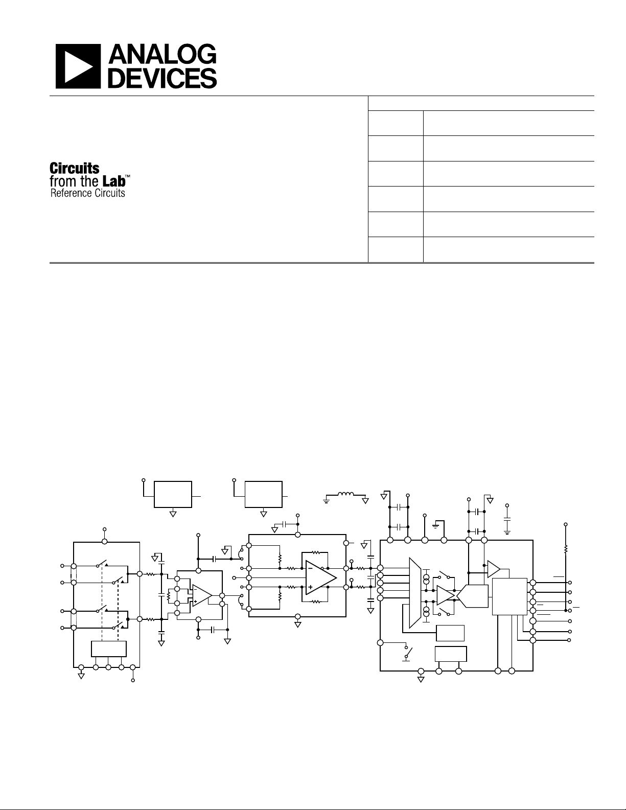
CIRCUIT FUNCTION AND BENEFITS
The circuit shown in Figure 1 is a flexible signal conditioning
circuit for processing signals of wide dynamic range, varying
from several mV p-p to 20 V p-p. The circuit provides the
necessary conditioning and level shifting and achieves the
dynamic range using the internal programmable gain amplifier
(PGA) of the high resolution analog-to-digital converter (ADC).
A ±10 V full-scale signal is very typical in process control and
industrial automation applications; howe v er, in some situations,
the signal can be as small as several mV. Attenuation and level
shifting is necessary to process a ±10 V signal with modern low
voltage ADCs. However, amplification is needed for small signals
to make use of the dynamic range of the ADC. Therefore, a
circuit with a programmable gain function is desirable when the
input signal varies over a wide range.
In addition, small signals may have large common-mode voltage
swings; therefore, high common-mode rejection (CMR) is required.
In some applications, where the source impedance is large, high
impedance is also necessary for the analog front-end input circuit.
ON
iCMOS Multiplexer
Low Cost, Wide Supply Range, Rail-to-Rail
Output, Instrumentation Amplifier
Precision, Selectable Gain, Fully
Differential Funnel Amplifier
4.8 kHz Ultralow Noise 24-Bit Sigma-Delta
ADC with PGA
50 mA, High Voltage, Micropower Linear
5 V Regulator
Ultralow Noise, LDO XFET Voltage
Reference with Current Sink and Source
Figure 1. Flexible Analog Front-End Circuit for Wide Industrial Range Signal Conditioning
engineers. Standard engineering practices have been employed in the design and construction of
suitability and applicability for your use a
One Technology Way, P.O. Box 9106, Norwood, MA 02062-9106, U.S.A.
Tel: 781.329.4700
www.analog.com
Page 2

CN-0251 Circuit Note
The circuit shown in Figure 1 solves all of these challenges
and provides programmable gain, high CMR, and high input
impedance. The input signal passes through the 4-channel
ADG1409 multiplexer into the AD8226 low cost, wide input
range instrumentation amplifier. The AD8226 offers high CMR
up to 80 dB and very high input impedance (800 MΩ differential
mode and 400 MΩ common mode). A wide input range and
rail-to-rail output allow the AD8226 to make full use of the
supply rails.
The AD8475 is a fully differential, attenuating amplifier with
integrated precision gain resistors. It provides precision attenuation
(G = 0.4 or G = 0.8), common-mode level shifting, and singleended-to-differential conversion. The AD8475 is an easy to use,
fully integrated precision gain block, designed to process signal
levels up to ±10 V on a single supply. Therefore, the AD8475 is
suitable for attenuating signals from the AD8226 up to 20 V p-p,
while maintaining high CMR and offering a differential output to
drive the differential input ADC.
The AD7192 is a 24-bit sigma-delta (Σ-Δ) ADC with an internal
PGA. The on-chip, low noise gain stage (G = 1, 8, 16, 32, 64, or
128) means that signals of large and small amplitude can be
interfaced directly to the ADC.
With the combination of the previous parts, the circuit offers
very good performance and easy configuration for signals
with varying amplitudes. The circuit can be used in industrial
automation, process control, instrumentation, and medical
equipment applications.
CIRCUIT DESCRIPTION
The circuit comprises of an ADG1409 multiplexer, an AD8226
instrumentation amplifier, an AD8475 difference amplifier, and an
AD7192 Σ-Δ ADC with an ADR444 reference, and the ADP1720
regulator. Only a few external components are used for protection,
filtering, and decoupling, making this circuit highly integrated, and
it requires a small circuit board (printed circuit board [PCB]) area.
Regulator and Reference Selection
The ADP1720-5 was chosen as the 5 V regulator for this circuit.
It is a high voltage micropower, low dropout linear regulator
suitable for industrial applications.
The 4.096 V ADR444 reference was chosen as the reference for
this circuit. It is an ultralow noise, high accuracy, low dropout
Table 1. Gain Configurations for the AD8475 and the AD7192 Internal PGA for Various Input Ranges
Input Range (VSxA − VSxB) Gain of AD8475 Gain of AD7192 PGA Output Range, Bipolar Mode (V)
±10 V 0.4 1 ±4
±5 V 0.8 1 ±4
±1 V 0.4 8 ±3.2
±500 mV 0.8 8 ±3.2
±250 mV 0.8 16 ±3.2
± 125 mV 0.8 32 ±3.2
±62.5 mV 0.8 64 ±3.2
±31.25 mV 0.8 128 ±3.2
device that is particularly suitable for high resolution, Σ-Δ ADCs
and precision data acquisition systems.
Input Switch and Protection
The ADG1409 multiplexer has 2-bit binary address lines that
are used to select one of four possible input channels. The design
also includes external protection such as standard diodes and
transient voltage suppressors to enhance the robustness of the
circuit. These are not shown in Figure 1; however, they are shown
in the detailed schematics and other documentation in the
CN0251 Design Support Package.
The ADG1409 multiplexer is configured to accept four
differential input signals: (VS1A − VS1B), (VS2A − VS2B),
(VS3A − VS3B), and (VS4A − VS4B). The outputs of the
multiplexer, DA and DB, are applied to the inputs of the
AD8226 in-amp.
AD8226 Input Instrumentation Amplifier
The external RG resistor sets the gain of the AD8226. For this
circuit, R
is omitted, and the gain of the in-amp stage is 1. The
G
output of the AD8226 is therefore VSxA − VSxB, where x is the
input channel number.
The differential input of the AD8226 is filtered by two 4.02 kΩ
resistors and a 10 nF capacitor, which form a single-pole RC filter
with a cutoff frequency of 2.0 kHz. The two 1 nF capacitors add
common-mode filtering with a cutoff frequency of 40 kHz.
AD7192 ADC PGA Gain Configuration
The AD7192 is configured to accept differential analog inputs
to match the differential output signals from the AD8475. The
full-scale input range of the AD7192 is ±V
±V
= REFINx(+) − REFINx(−).
REF
/gain, where
REF
When the buffer in the AD7192 is enabled, the input channel
drives the high impedance input stage of the buffer amplifier, and
the absolute input voltage range in this mode is restricted to a
range of AGND + 250 mV and AV
− 250 mV. When the gain
DD
stage is enabled, the output from the buffer is applied to the input
of the PGA, and the analog input range must be limited to
±(AV
− 1.25 V)/gain because the PGA requires additional
DD
headroom. Therefore, with a 4.096 V reference and a 5 V power
supply, and to make the maximum use of the dynamic range of the
ADC, the signal can be attenuated or amplified as shown in Table 1.
Rev. 0 | Page 2 of 6
Page 3

Circuit Note CN-0251
t
= 3/f
t
= 4/f
Differential Attenuating Amplifier
To drive the low voltage ADCs, the ±10 V or ±5 V signals
require attenuation and level shifting. A difference amplifier
configuration in conjunction with precision resistors inevitably
degrades CMR performance due to the mismatch between the
resistors. The AD8475 level shifter/attenuator integrates matched,
precision, laser trimmed resistors to ensure low gain error, a low
gain drift (3 ppm/°C maximum), and high CMR.
The AD8475 has pin-selectable gain options of 0.4 and 0.8. The
VOCM pin adjusts the output voltage common mode for precision
level shifting to match the input range of the ADC and to maximize
the dynamic range. This pin can be left floating and is internally
biased with a precision voltage divider consisting of two 200 kΩ
resistors between the supplies and ground, thereby providing
the midsupply voltage on the pin.
Table 2. Output Data Rate and Settling Time for Different Configurations
Chopper Filter Option SINC3 SINC4
Disabled f
Enabled f
t
ADC
SETT LE
ADC
SETT LE
= f
/(1024 × FS[9:0]) f
CLK
ADC
= f
/(3 × 1024 × FS[9:0]) f
CLK
= 2/f
t
ADC
A single-pole differential RC filter composed of two 100 Ω
resistors and a 1 µF capacitor serves as an antialiasing and noise
reduction filter for the AD7192 with a cutoff frequency of 800 Hz.
The two 10 nF capacitors provide common-mode filtering with
a cutoff frequency of 160 kHz.
Filter, Output Data Rate, and Settling Time
The AD7192 Σ-Δ ADC consists of a modulator followed by a
digital filter. The output data rate (f
) and settling time (t
ADC
SETTLE
are related to the filter configuration and the chop configuration.
Table 2 shows the output data rates and settling time
calculations for different configurations.
= f
ADC
SETT LE
ADC
SETT LE
/(1024 × FS[9:0])
CLK
ADC
= f
/(4 × 1024 × FS[9:0])
CLK
= 2/f
ADC
)
Rev. 0 | Page 3 of 6
Page 4

CN-0251 Circuit Note
0 50
26.0
25.5
25.0
24.5
24.0
23.5
23.0
22.5
22.0
21.5
100 150 200 250
SAMPLE NUMBER
NOISE OUTPUT (µV)
300 350 400 450 500
10351-002
7FFF9C
140
120
100
80
60
40
20
0
7FFF9D
7FFF9E
7FFF9F
7FFFA0
CODE (HEX)
OCCURENCES
7FFFA1
7FFFA2
10351-003
5
960
4.17
20.9
19.8
18.9
18.0
17.2
16.2
Layout Considerations
The performance of this or any other high speed or high
resolution circuit is highly dependent on proper PCB layout.
This includes, but is not limited to, power supply bypassing,
signal routing, and proper power planes and ground planes. See
Tutor i al MT-031, Tut o r ia l MT-101, and the article A Practical
Guide to High-Speed Printed-Circuit-Board Layout for more
detailed information regarding PCB layout.
System Performance
The 24-bit AD7192 Σ-Δ ADC offers very good performance in
this circuit. See the Tut or ia l M T-022 and the Tutori a l MT-023 for
more detailed information regarding the Σ-Δ ADCs.
With the configuration set to chop disabled, an output data rate
of 4.7 Hz, a gain of 1, and a SINC4 filter, Figure 2 shows the noise
performance, and Figure 3 shows the noise distribution histogram
with 500 samples. The measured peak-to-peak noise of this
circuit is approximately 3.9 µV (see Figure 2), and the rms noise
is 860 nV. This corresponds to a peak-to-peak (noise-free code)
resolution of 20 bits and an rms resolution of 23 bits. Ta bl e 3
shows the rms noise for some of the data rates and gain settings
of the AD7192 with chop disabled and a SINC4 filter.
Figure 2. Noise Output (V
Gain = 1, Chop Disabled, SINC4 Filter)
= 4.096 V, AVDD = 5 V, Output Data Rate = 4.7 Hz,
REF
Figure 3. Noise Histogram (V
= 4.096 V, AVDD =5 V, Output Data Rate = 4.7
REF
Hz, Gain = 1, Chop Disabled, SINC4 Filter)
Table 3. RMS Resolution of the System with Different Output Data Rates and Gain Settings of the AD7192 with Chop Disabled and
a SINC4 Filter (Subtract 2.7 Bits to Get Peak-to-Peak or Noise-Free Code Resolution)
Filter Word (Decimal) Output Data Rate (Hz) Settling Time (ms) Gain 1 Gain 8 Gain 16 Gain 32 Gain 64 Gain 128
1023 4.7 852.5 23.0 21.8 20.4 19.7 18.8 17.4
640 7.5 533 22.5 21.5 20.0 19.5 18.5 17.2
96 50 80 22.3 20.9 19.8 19.3 18.2 17.0
16 300 13.3 21.8 20.2 19.3 18.6 17.6 16.8
1 4800 0.83 19.2 19.0 18.4 17.6 16.6 15.8
Rev. 0 | Page 4 of 6
Page 5

Circuit Note CN-0251
TRIPLE POWER SUPPLY
PC
USB
USB
SDP
+15V –15V GND GND +6V
J3-1
VIN+
120-PIN SD P CONNE CTOR
SDP CONA OR CONB
SIGNAL SOURCE
VIN–
J1-2
EVAL-CN0251-SDPZ
J4
J1-1
J3-3 J3-2 J2-2 J2-1
10351-004
COMMON VARIATIONS
Other 24-bit or lower resolution Σ-Δ ADCs with integrated
PGAs can be used, such as the AD7190, AD7193, AD7797, and
AD7799. If no attenuation for the input signal is required, the
AD8476 can be used for lower power than the AD8475.
In applications where there is no need for attenuation and high
input impedance, the AD7192 can be connected directly to the
sensor to avoid noise introduced by the analog front-end
conditioning circuits. For instance, a load cell with a small full-scale
output voltage does not require attenuation and can be connected
directly to the AD7192 differential inputs (see CN-0102,
CN-0107, CN-0108, CN-0118, CN-0119, and CN-0155)
CIRCUIT EVALUATION AND TEST
The circuit test setup uses the E VA L-CN0251-SDPZ circuit
evaluation board and the System Demonstration Platform (SDP)
evaluation board (E VA L-SDP-CB1Z). The two boards have 120-pin
mating connectors, allowing for the quick setup and evaluation
of the performance of the circuit. The EVA L-CN0251-SDPZ
board contains the circuit to be evaluated, as described in this
circuit note, and the SDP is used with the CN-0251 evaluation
software to capture the data from the EVA L-CN0251-SDPZ.
The SDP is also used to control the input multiplexer and
various functions within the AD7792 ADC.
Equipment Needed
The following equipment is needed:
• A PC with a USB port and Windows XP or Windows Vista
(32-bit) or Windows 7 (32-bit)
• An E VA L-CN0251-SDPZ circuit evaluation board
• An E VA L- SDP-CB1Z SDP evaluation board
• A dc supply: +15 V, −15 V, a nd + 6 V.
• CN-0251 evaluation software
Getting Started
Load the evaluation software by placing the CN-0251 evaluation
software CD in the CD drive of the PC. Then, locate the drive
that contains the evaluation software CD and open the Readme
file. Follow the instructions contained in the Readme file for
installing and using the evaluation software.
Functional Block Diagram
Figure 4 shows a functional block diagram of the test setup. The
E VA L-CN0251-SDPZ-SCH.pdf file has the detailed schematics
for the EVA L-CN0251-SDPZ. This file is contained in the CN0251 Design Support Package: www.analog.com/CN0251-
DesignSupport.
Figure 4. Test Setup Functional Block Diagram
Setup
Connect the 120-pin connector on the E VA L-CN0251-SDPZ to
the CO NA connector on the E VA L -SDP-CB1Z (SDP). Use nylon
hardware to firmly secure the two boards, using the holes provided
at the ends of the 120-pin connectors. After successfully setting
the dc output supply to the +15 V, −15 V, and +6 V output, turn
the power supply off.
With power to the supply off, connect a +15 V power supply to
the +15VA pin of J3, a −15 V power supply to the −15VA pin of
J3, and GND to the AGND pin of J3. Also, with power to the
supply off, connect 6 V to J2. Turn on the power supply and then
connect the USB cable with the SDP to the USB port on the PC.
Do not connect the USB cable to the mini-USB connector on
the SDP before turning on the dc power supply for the EVA L-
CN0251-SDPZ.
Test
After setting up the power supply and connecting to EVA L-
CN0251-SDPZ, launch the evaluation software and connect the
USB cable from the PC to the mini-USB connector on the SDP.
The software is able to communicate to the SDP if the Analog
Devices System Development Platform driver is listed in the
Device Manager.
Once USB communications are established, the SDP can now
be used to send, receive, and capture serial data from the EVA L -
CN0251-SDPZ. Then, connect the signal source for measurements.
Information regarding the SDP can be found at
www.analog.com/SDP.
Rev. 0 | Page 5 of 6
Page 6

CN-0251 Circuit Note
(Continued from first page ) Circuits from the Lab circuits are intended only for use with Analog Devices products and are the intellectual property of Analog Devices or its licensors. While you
reserves the right to change any Circuits from the Lab circuits at any time without notic e but is under no obligation to do so.
registered trademarks are the property of their respective owners.
LEARN MORE
MT-031 Tutorial, Grounding Data Converters and Solving the
Mystery of “AGND” and “DGND”, Analog Devices.
MT-073 Tutorial, High Speed Variable Gain Amplifiers (VGAs),
Analog Devices.
MT-101 Tutorial, Decoupling Techniques, Analog Devices.
MT-022 Tutorial, ADC Architectures III: Sigma-Delta ADC
Basics, Analog Devices.
MT-023 Tutorial, ADC Architectures IV: Sigma-Delta ADC
Advanced Concepts and Applications, Analog Devices.
Data Sheets and Evaluation Boards
CN-0251 Circuit Evaluation Board (EVAL-CN0251-SDPZ)
System Demonstration Platform (EVAL-SDP-CB1Z)
AD8226 Data Sheet
AD8475 Data Sheet
AD7192 Data Sheet
ADG1409 Data Sheet
ADR444 Data Sheet
ADP1720 Data Sheet
REVISION HISTORY
6/12—Rev. 0: Initial Version
may use the Circuits from the Lab circuits in the design of your product, no other license is granted by implication or otherwise under any patents or other intellectual property by
application or use of the Circuits from the Lab circuits. Information furnished by Analog Devices is believed to be accurate and reliable. However, Circuits from the Lab circuits are supplied
"as is" and without warranties of any kind, express, implied, or statutory including, but not limited to, any implied warranty of merchantability, noninfringement or fitness for a particular
purpose and no responsibility is assumed by Analog Devices for their use, nor for any infringements of patents or other rights of third parties that may result from their use. Analog Devices
©2012 Analog Devices, Inc. All rights reserved. Trademarks and
CN10351-0-6/12(0)
Rev. 0 | Page 6 of 6
 Loading...