

Page 1

Circuit Note
CN-0245
Wideband Synthesizer with
Integrated VCO
400 MHz to 6 GHz Quadrature
Demodulator
0
its from Analog Devices have been designed and built by Analog Devices
engineers. Standard engineering practices have been employed in the design and construction of
room temperature. However, you are solely responsible for testing the circuit and determining its
suitability and applicability for your use and application. Accordingly, in no event shall Analog Devices
or direct, indirect, special, incidental, consequential or punitive damages due to any cause
whatsoever connected to the use of any Circuits from the Lab circuits. (Continued on last page)
Fax: 781.461.3113 ©2011 Analog Devices, Inc. All rights reserved.
0°
90°
LOIP
LOIN
ADF4350
ADL5380/ADL5387
QUADRATURE DEMODULATOR
WIDEBAND
SYNTHESIZER
RF
OUT
A+
RF
OUT
A–
LPF
3.3V
RF+ RF–
Q+
Q–
I+
I–
Z
BIAS
Z
BIAS
10224-001
Devices Connected/Referenced
Circuits from the Lab™ reference circuits are engineered and
tested for quick and easy system integration to help solve today’s
analog, mixed-signal, and RF design challenges. For more
information and/or support, visit www.analog.com/CN0245.
Wideband LO PLL Synthesizer with Simple Interface to Quadrature Demodulators
ADF4350
ADL5387 50 MHz to 2 GHz Quadrature Demodulator
ADL5380
EVALUATION AND DESIGN SUPPORT
Circuit Evaluation Boards
ADL5387 Evaluation Board (ADL5387-EVALZ)
ADL5380 Evaluation Board (ADL5380-30A-EVALZ)
CN0134 Evaluation Platform (CFTL-CN0134-EVALZ)
Design and Integration Files
Schematics, Layout Files, Bill of Materials
CIRCUIT FUNCTION AND BENEFITS
The circuit, shown in Figure 1, highlights the ease of interfacing
the ADF4350 wideband synthesizer with integrated VCO with
the ADL5380 and ADL5387 wideband I/Q demodulators. In
this circuit, the ADF4350 provides the high frequency, low
phase noise local oscillator (LO) signal to the wideband I/Q
demodulator.
This circuit configuration offers quite a few benefits that make
it an attractive solution in applications requiring quadrature
mixing down to baseband or to an intermediate frequency.
The ADF4350 offers RF differential outputs and, likewise, the
ADL5380/ADL5387 accept differential inputs. This interface
offers both ease of use and performance advantages. The
differential signal configuration provides common-mode noise
reduction and even order cancellation of the LO harmonics,
which maintains the quadrature accuracy of the I/Q
demodulators. Additionally, the output power level of the
ADF4350 matches the input power requirements of the
quadrature demodulators very well. As a result, an LO buffer is
not necessary.
The ADF4350 outputs cover a wide frequency range from
137.5 MHz to 4400 MHz. The ADL5387 frequency range spans
from 50 MHz to 2 GHz, and the ADL5380 covers the higher
frequency range from 400 MHz to 6 GHz. Between the
ADL5380 and ADL5387 the RF input range can span from
50 MHz to 6 GHz. Therefore, the two chip circuit configuration
as shown in Figure 1 offers coverage of a wide frequency range
from 50 MHz to 4400 GHz.
Figure 1. Simple Interface Between the ADF4350 PLL Synthesizer and the ADL5380 or ADL5387 Quadrature Demodulator
Rev.
Circuits from the Lab™ circu
each circuit, and their function and performance have been tested and verified in a lab environment at
be liable f
(Simplified Schematic: All Connections and Decoupling Not Shown)
One Technology Way, P.O. Box 9106, Norwood, MA 02062-9106, U.S.A.
Tel: 781.329.4700
www.analog.com
Page 2
CN-0245 Circuit Note
D Q
Q
LO_IN
CK
D Q
QCK
LO_I (0°)
LO_Q (90°)
10224-002
LO_I (0°)
LO_Q (90°)
LO_IN
10224-003
ADF4350
WIDEBAND
SYNTHESIZER
RF
OUT
A+
RF
OUT
A–
3.3V
Z
BIAS
Z
BIAS
12
13
ADL5387
QUADRATURE
DEMODULATOR
LOIP
LOIN
3
4
10224-004
CIRCUIT DESCRIPTION
The ADF4350 is a wideband fractional-N and integer-N phaselocked loop frequency synthesizer covering the frequency range
of 137.5 MHz to 4400 MHz. The ADF4350 has an integrated
voltage controlled oscillator (VCO) with a fundamental
frequency range of 2200 MHz to 4400 MHz. The ADF4350
offers high quality synthesizer performance. However,
depending on the demodulator architecture, LO filtering may
be required to minimize the effects of harmonics from the PLL
on the quadrature accuracy of the I/Q demodulator.
Analog Devices offers quadrature demodulators that cover a
wide frequency range. The ADL5387 frequency range spans
from 50 MHz to 2 GHz, and the ADL5380 covers the higher
frequency range from 400 MHz to 6 GHz. The ADL5387 and
ADL5380 utilize two different architectures to generate the 90°
phase shift between the I and Q paths. The ADL5387 utilizes a
2 × LO architecture where the local oscillator is at twice the RF
frequency, while the ADL5380 uses a polyphase filter-based
phase splitter. The polyphase architecture has a narrower
fractional bandwidth (i.e., operates across less octaves) and is
more sensitive to PLL harmonics compared to a 2 × LO-based
phase splitter. As a result, the ADL5380 requires harmonic
filtering of the LO to maintain the quadrature accuracy of
the I/Q demodulator, while filtering is only required for the
2 × LO-based ADL5387 at the top end of its frequency range.
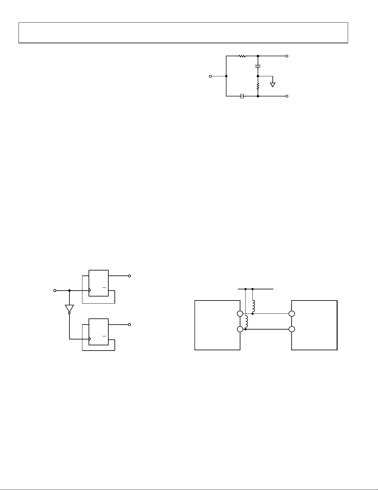
Figure 3. Simplified First Order Polyphase Filter
Figure 3 shows a simplified first order polyphase circuit, as
implemented in the ADL5380. The polyphase circuit consists of
complementary RC subcircuits that create a low-pass transfer
function from input to one output, and a high-pass transfer
function to the other output. If the R and C values of the two
polyphased paths are matched, then both paths have the same
corner frequency and, more importantly, the phase of one
output tracks the other with a 90° phase shift.
Interfacing the ADF4350 PLL with the ADL5387 I/Q Demodulator
The ADL5387 and ADL5380 I/Q demodulators utilize different
architectures to achieve the ultimate goal of generating precise
quadrature signals. When interfacing with an LO synthesizer
like the ADF4350, it is important to consider how the
architectures respond to the LO signal and its harmonics.
This will determine the requirement for LO filtering. Figure 4
shows the basic interface between the ADF4350 and ADL5387.
Depending on the frequency of operation, an LO harmonic
filter may or may not be required between the ADF4350
and ADL5387.
Figure 2. Simplified 2 × LO-Based Phase Splitter
Figure 2 shows a simplified 2 × LO phase splitter as
implemented in the ADL5387. The 90° phase split of the LO
path is achieved via digital circuitry that uses D-type flip-flops
and an inverter. This architecture requires an external LO
operating at twice the frequency of the desired LO.
Figure 4. ADF4350 PLL Interface to the 2 × LO-Based Phase Splitter of the
ADL5387 Demodulator
In a 2 × LO-based phase splitter, the quadrature accuracy is
dependent on the duty cycle accuracy of the incoming LO.
The matching of the internal divider flip-flops also affects
quadrature accuracy but to a much lesser extent. So a 50% duty
cycle of the externally applied LO is critical for minimizing
quadrature errors. Additionally, any imbalance in the rise and
fall times causes even order harmonics to appear. When
driving the demodulator LO inputs differentially, even order
cancellation of the harmonics is achieved and results in
improved overall quadrature generation.
Rev. 0 | Page 2 of 5
Page 3

Circuit Note CN-0245
–20
–70
425 1225
10224-005
IMAGE REJECTION (dBc)
RF FREQUENCY (MHz)
–25
–30
–35
–40
–45
–50
–55
–60
–65
525 625 725 825 925 1025 1125
ADF4350, NO FILTER
SIGNAL GENERATOR
ADF4350 + FIL TER
ADF4350
WIDEBAND
SYNTHESIZER
RF
OUT
A+
RF
OUT
A–
LPF
3.3V
Z
BIAS
Z
BIAS
12
13
ADL5380
QUADRATURE
DEMODULATOR
LOIP
LOIN
3
4
10224-006
–10
–70
850
10224-007
–20
–30
–40
–50
–60
1350 1850
2350
IMAGE REJECTION (dBc)
RF FREQUENCY (MHz)
ADF4350, NO FILTER
SIGNAL GENERATOR
ADF4350 + FIL TER
With a target image suppression of −40 dBc, Figure 5 shows the
performance of the ADL5387 with the ADF4350 providing the
differential LO source with and without filtering. The blue
signal trace representing the “Signal Generator” is the ideal case
where the LO is generated using a Rhode & Schwarz signal
generator with a sinusoidal output and much lower harmonic
levels compared to the ADF4350. This is the ideal case and the
target comparison point. From Figure 5, it can be seen that
filtering is not required at frequencies below 1 GHz. However,
above 1 GHz small errors due to harmonics of the LO become a
larger percentage of the input period. In this case, filtering
should be used to further attenuate the even order harmonics of
the LO and so that the I/Q demodulator’s specified quadrature
accuracy can be achieved.
Interfacing the ADF4350 PLL with the ADL5380 Quadrature Demodulator
Unlike the ADL5387, the polyphase architecture of the
ADL5380's phase splitter requires filtering of the ADF4350
outputs, as shown in Figure 6. Filtering is required to attenuate
the odd order harmonics of the LO to minimize errors in the
quadrature generation block of the ADL5380. From
measurement and simulation as explained in CN-0134, the odd
order harmonics contribute more than even order harmonics to
quadrature errors. Figure 7 shows the measurement results
when the ADF4350 outputs are filtered before they are applied
to the differential LO inputs of the ADL5380. After filtering, the
resulting image rejection is comparable to what is achievable
from a low harmonic signal generator.
Figure 5. ADL5387 Image Rejection vs. RF Frequency
Figure 6. ADF4350 Interface to the Polyphase Filter Architecture of the
ADL5380 Demodulator
Figure 7. ADFL5380 Image Rejection vs. Frequency.
Filtering Requirements
In summary, LO filtering the ADF4350 outputs to suppress the
harmonics of the fundamental helps to maintain the phase
accuracy of the quadrature signals of the demodulator. In the
case of the ADL5380, which uses a polyphase architecture,
filtering is a requirement. The ADL5387 architecture consists of
digital circuitry which is more immune to the harmonics of the
LO signal. Therefore filtering may not be required, depending
on the frequency of operation.
In the case where filtering is necessary, Figure 8, shows an
example LO output filter schematic, and Table 1, summarizes
the filter component values. This circuit is flexible and provides
four different filter options to cover four different bands The
filters were designed for a 100 Ω differential input and 50 Ω
differential output to match the LO input requirements of the
demodulator. A Chebyshev response was used for optimal filter
roll-off at the expense of increased pass-band ripple. Please
refer to CN-0134 for a more detailed discussion on the filtering
of the ADF4350 outputs.
Rev. 0 | Page 3 of 5
Page 4

CN-0245 Circuit Note
Table 1. ADF4350 RF Output Filter Component Value (DNI = Do Not Insert)
Frequency Range
(MHz) Z
BIAS
a. 500–1300 27 nH|| 50 Ω 3.9 3.9 DNI 4.7 DNI 5.6 DNI 3.3
b. 850–2450 19 nH || (100 Ω in position C1c) 2.7 2.7 3.3 100 Ω 4.7 DNI 3.3 DNI
c. 1250–2800 50 Ω 0 Ω 3.6 DNI DNI 2.2 DNI 1.5 DNI
d. 2800–4400 3.9 nH 0 Ω 0 Ω DNI DNI DNI DNI DNI DNI
3.3V
120pF 120pF
RF
RF
12
A+
OUT
A–
13
OUT
Figure 8. ADF4350 RF Output Filter Schematic
0.1µF
C1a C2a C3a
Z
BIAS
Z
BIAS
L1 L2
C1c C2c C3c
L1 L2
C1a C2a C3a
1nF
1nF
3
4
COMMON VARIATIONS
The interface discussed above is applicable to any PLL with
differential LO outputs and to any 1 × LO or 2 × LO-based I/Q
demodulator. The ADL5382 is a 1 × LO-based I/Q demodulator
that operates from 700 MHz to 2700 MHz and provides slightly
higher IP3 than the ADL5380. TheAD8347 (1 × LO) and
AD8348 (2 × LO) are lower power I/Q demodulators that
integrate front-end variable gain amplifiers and fixed-gain
baseband amplifiers.
CIRCUIT EVALUATION AND TEST
The circuits shown in Figure 4 and Figure 6 were implemented
using the CN-0134 evaluation board (CFTL-0134EVALZ) and
the ADL5387 or ADL5380 evaluation boards. The CN-0134
evaluation platform includes the ADF4350, pads for an LO
filter, and differential LO outputs to SMA connectors.
The ADF4350 must be programmed, and the software is
contained on the CD that accompanies the evaluation board.
Table 2 provides the ordering guide for the various evaluation
boards.
The CN-0134 evaluation board is configured by default to an
850 MHz to 2450 MHz filter design as specified in Table 1. To
implement an alternative filter, the appropriate components
must be swapped out.
LOIP
LOIN
ADL5380ADF4350
L1
(nH)
L2
(nH)
C1a
(pF)
C1c
(pF)
C2a
(pF)
C2c
(pF)
C3a
(pF)
C3c
(pF)
Table 2. Evaluation Board Information
Evaluation Board
ADL5387 ADL5387-EVALZ
ADL5380
Low Band (400 MHz to 3 GHz)
Mid Band (3 GHz to 4 GHz)
ADL5380-30A-EVALZ
ADL5380-29A-EVALZ
CN-0134 CFTL-0134-EVALZ
Equipment Needed
10224-008
• Windows XP, Windows Vista (32-bit), or Windows 7
(32-bit) PC with USB port
• Evaluation boards as listed in Table 2
• RF source (Rohde & Schwarz SMT06 or equivalent)
• Spectrum analyzer (Rohde & Schwarz FSEA30 or
equivalent)
• Power supplies:
• ADL5387-EVA L Z: +5 V
• ADL5380-30A-EVA LZ : +5 V
• CFTL-0134-EVA LZ : +5.5 V
Test
The CN-0134 evaluation platform allows easy evaluation and
has an integrated crystal oscillator on board. A PC with the
ADF4350 software is required to program the synthesizer to the
desired LO frequency. The ADL5387/ADL5380 quadrature
demodulator will downconvert the RF frequency to baseband.
The differential I and Q baseband outputs are applied to the
FSEA spectrum analyzer in the FFT mode, and image rejection
is measured.
Additional documentation can be found in the following design
support packages for CN-0245, CN-0134, and CN-0144:
CN-0245 Design Support Package:
www.analog.com/CN0245-DesignSupport
CN-0134 Design Support Package:
www.analog.com/CN0134-DesignSupport
CN-0144 Deign Support Package:
www.analog.com/CN0144-DesignSupport
Rev. 0 | Page 4 of 5
Page 5

Circuit Note CN-0245
ROHDE & SCHWARZ
SMT06 SIG NAL GENERATOR
USB
PC CONTROLLER
CN-0134
EVALUATION PLATFORM
(CFTL-0134-EVALZ)
E3631 POWER SUPPLY
Figure 9. F
LEARN MORE
Nash, Eamon, AN-1039 Application Note. Correcting
Imperfections in IQ Modulators to Improve RF Signal
Fidelity. Analog Devices.
CN-0245 Design Support Package:
www.analog.com/CN0245-DesignSupport
CN-0134 Design Support Package:
www.analog.com/CN0134-DesignSupport
CN-0144 Design Support Package:
www.analog.com/CN0144-DesignSupport
ADIsimRF Design Tool
ADIsimPLL Design Tool
LO+
ADL5380 OR ADL5387
LO–
AGILENT
EVALUATION BOARD
+5.0V+5.5V
unctional Block Diagram of Test Setup
Data Sheets and Evaluation Boards
ADL5387 Data Sheet and Evaluation Board
ADL5380 Data Sheet and Evaluation Board
ADF4350 Data Sheet and Evaluation Board
REVISION HISTORY
12/11—Revision 0: Initial Version
RF
I+
I–
Q+
Q–
ROHDE & SCHWARZ
FSEA30 SPECT RUM ANALYZER
10224-009
(Continued from first page) Circuits from the Lab circuits are intended only for use with Analog Devices products and are the intellectual property of Analog Devices or its licensors. While
you may use the Circuits from the Lab circuits in the design of your product, no other license is granted by implication or oth
application or use of the Circuits from the Lab circuits. Information furnished by Analog Devices is believed to be accurate and reliable. However, Circuits from the Lab designs are supplied
"as is" and without warranties of any kind, express, implied, or statutory including, but not limited to, any implied warranty of merchantability, noninfringement or fitness for a particular
purpose and no responsibility is assumed by Analog Devices for their use, nor for any infringements of patents or other rights of th ird parties that may result from their use. Analog Devices
reserves the right to change any Circuits from the Lab circuits at any time without notic e but is under no obligation to do so.
©2
nalog Devices, Inc. All rights reserved. Trademarks and
011 A
registered trademarks are the property of their respective owners.
CN
10224-0-12/11(0)
erwise under any patents or other intellectual property by
Rev. 0 | Page 5 of 5
 Loading...