

Page 1
Circuit Note
ration to help solve today’s
AD7920
250 kSPS, 12-bit, 250 kSPS ADC in 6-Lead SC70
Rev. A
ts from Analog Devices have been designed and built by Analog Devices
engineers. Standard engineering practices have been employed in the design and construction of
room temperature. However, you are solely responsible for testing the circuit and determining its
suitability and applicability for your use and application. Accordingly, in no event shall Analog Devices
whatsoever connected to the use of any Circuits from the Lab circuits. (Continued on last page)
Fax: 781.461.3113 ©2012 Analog Devices, Inc. All rights reserved.
0.1Ω
2Ω
LOAD
1kΩ
64.9kΩ
210kΩ
470pF 1µF
1µF
+5V
1kΩ
+5V*
20kΩ
AD7920
ADP3336
SDP BOARD
ADA4096-2
GND
V
DD
V
IN
OPTIONAL FILTER
SCLK
SDATA
CS
+5V
SD
FB
GND
OUT
IN
+6V IN
+V
–V
R
C
+5V/2.5A
INPUT
SUPPLY
*SEE TEXT
V
A
V
B
V
OUT
20kΩ
10155-001
Circuits from the Lab™ reference circuits are engineered and
tested for quick and easy system integ
analog, mixed-signal, and RF design challenges. For more
information and/or support, visit www.analog.com/CN0241.
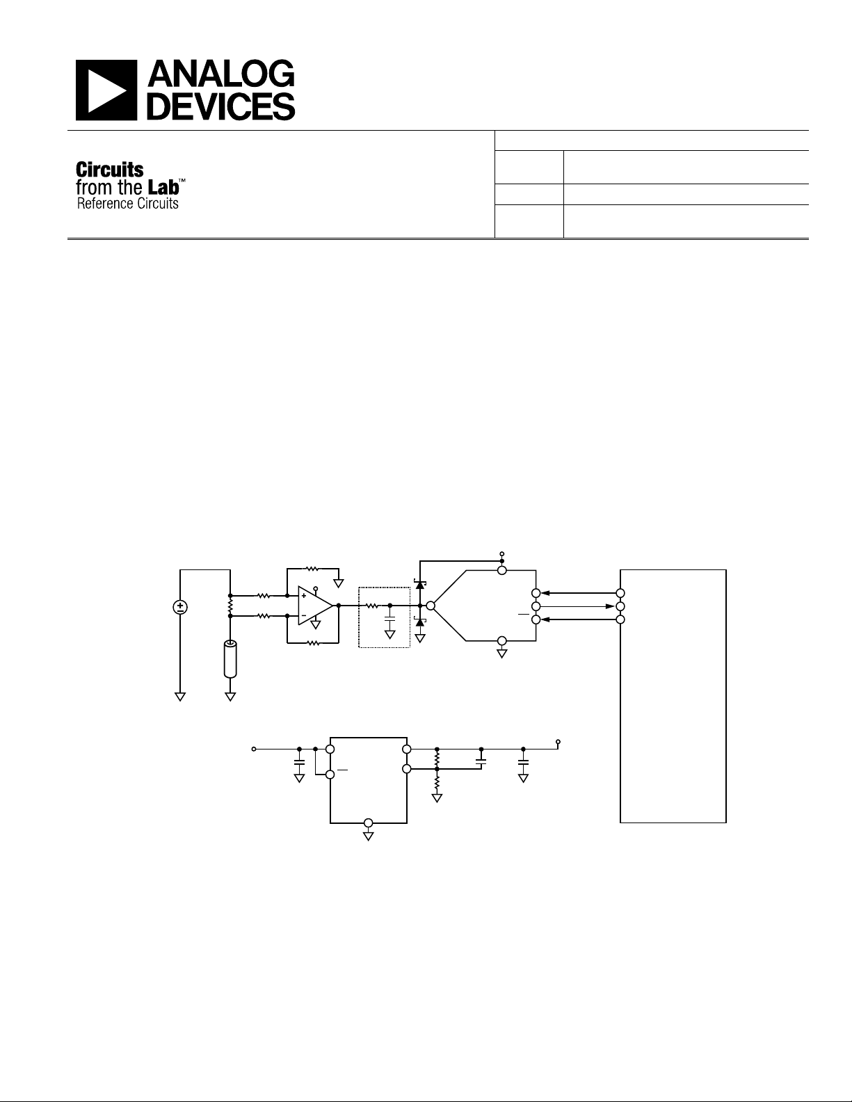
High-Side Current Sensing with Input Overvoltage Protection
EVALUATION AND DESIGN SUPPORT
Circuit Evaluation Boards
CN-0241 Circuit Evaluation Board (EVAL-CN0241-SDPZ)
System Demonstration Platform (EVAL-SDP-CB1Z)
Design and Integration Files
Schematics, Layout Files, Bill of Materials
CIRCUIT FUNCTION AND BENEFITS
High-side current monitors are likely to encounter overvoltage
conditions from transients or when the monitoring circuits are
connected, disconnected, or powered down. This circuit, shown
CN-0241
Devices Connected/Referenced
ADA4096-2
ADP3336
in Figure 1, uses the overvoltage protected ADA4096-2 op amp
connected as a difference amplifier to monitor the high-side
current. The ADA4096-2 has input overvoltage protection,
without phase reversal or latch-up, for voltages of 32 V higher
than and lower than the supply rails.
The circuit is powered by the ADP3336 adjustable low dropout
500 mA linear regulator, which can also be used to supply power to
other parts of the system, if desired. Its input voltage can range
from 5.2 V to 12 V when set for a 5 V output. To save power,
the current sensing circuit can be powered down by removing
power to the ADP3336; however, the power source, such as a
solar panel, can still operate.
30 V, Micropower, Overvoltage Protection,
Rail-to-Rail Input/Output Amplifier
High Accuracy Ultralow IQ 500 mA anyCAP®
Adjustable Low Dropout Linear Regulator
Circuits from the Lab™ circui
each circuit, and their function and performance have been tested and verified in a lab environment at
be liable for direct, indirect, special, incidental, consequential or punitive damages due to any cause
Figure 1. High-Side Current Sensing with Input Overvoltage Protection (Simplified Schematic: All Connections and Decoupling Not Shown)
One Technology Way, P.O. Box 9106, Norwood, MA 02062-9106, U.S.A.
Tel: 781.329.4700
www.analog.com
Page 2
CN-0241 Circuit Note
R6
V
CC
+IN
–IN
V
EE
OVP
OVP
OUT
R7
D10 Q20
Q19
D11
Q16
D7Q15
D8
Q14
Q17
Q10
Q13
Q18D9
×1
I3
R2
R1
R3
R4
C2
Q12
D6
R5
Q9
Q11
Q6
Q8Q7
Q5
Q4
Q3
Q1 Q2
I2
I1
C1
D3
D1
D4
D2
10155-002
7
–48 –40 –32 –24 –16 –8 0 8 16 24 32 40 48
–7
–6
–5
–4
–3
–2
–1
0
1
2
3
4
5
6
INPUT BIAS CURRE NT (mA)
VIN (V)
V
EE
= –15V
V
EE
= 0V
V
CC
= +15V
LOW RDS
ON
SERIES FET
5kΩ SERIES RESISTOR
10155-003
This applies voltage to the inputs of the unpowered ADA4096-2;
however, no latch-up or damage occurs for input voltages up to
32 V. If slower throughput rates are required, the AD7920 can
also be powered down between samples. The AD7920 draws a
maximum of 5 µW when powered down and 15 mW when
powered up. The ADA4096-2 requires only 120 µA under
operational conditions. When operating at 5 V, this is only
0.6 m W. Th e ADP3336 draws only 1 µA in the shutdown mode.
CIRCUIT DESCRIPTION
The circuit is a classic high-side current sensing circuit topology
with a single sense resistor. The other four resistors (dual 1 kΩ/
20 kΩ divider) are in a thin film network (for ratio matching)
and are used to set the difference amplifier gain. This amplifies
the difference between the two voltages seen across the sense
resistor and rejects the common-mode voltage.
V
= (VA − VB) (20 kΩ/1 kΩ)
OUT
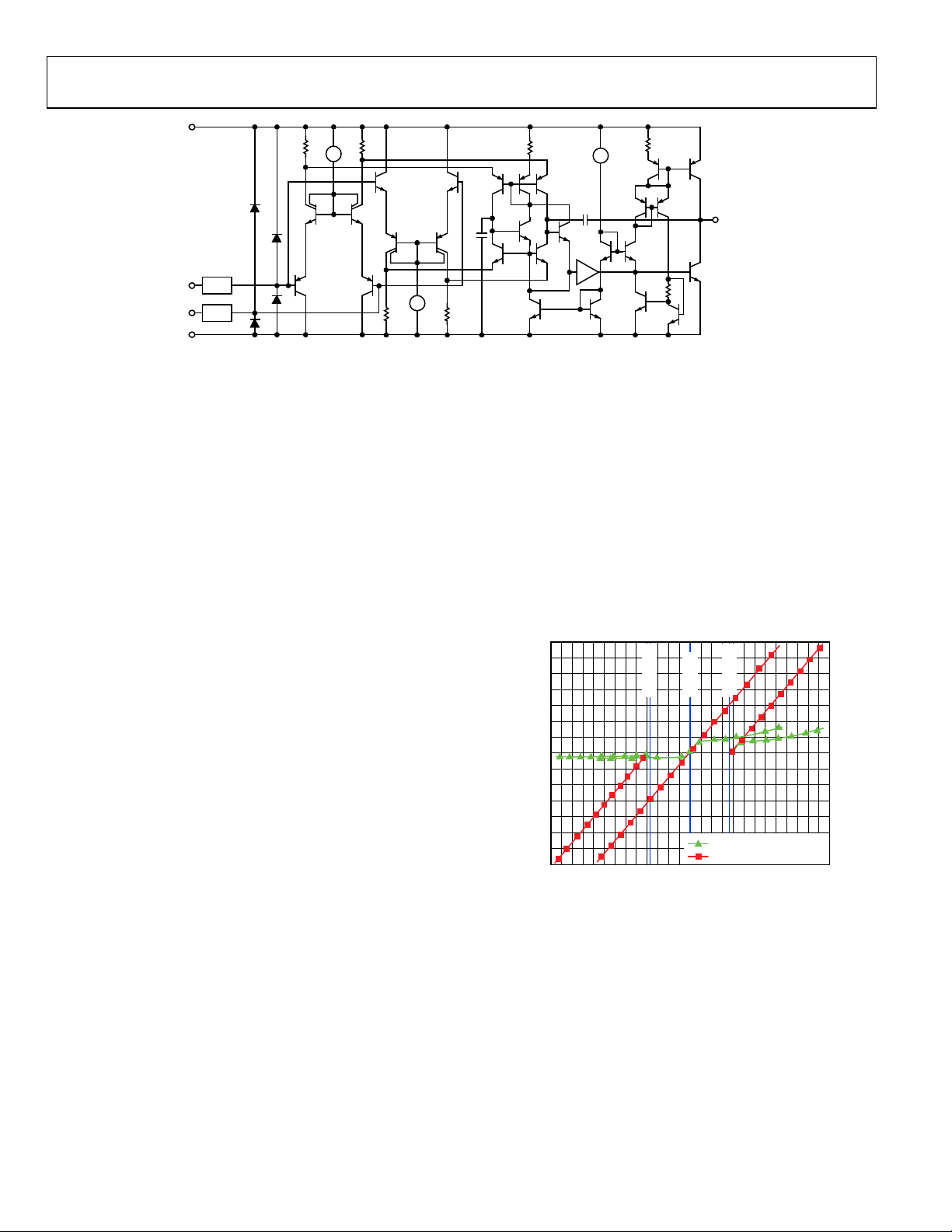
Figure 2 shows a simplified schematic of the ADA4096-2. The
input stage comprises two differential pairs (Q1 to Q4 and Q5 to
Q8) operating in parallel. When the input common-mode voltage
approaches V
minimum voltage compliance. Conversely, when the input
common-mode voltage approaches V
down as I2 reaches its minimum voltage compliance. This topology
allows for maximum input dynamic range because the amplifier
can function with its inputs at 200 mV outside the rail (at room
temperature).
As with any rail-to-rail input amplifier, V
the two input pairs determines the CMRR of the amplifier. If the
input common-mode voltage range is within 1.5 V of each rail,
transitions between the input pairs are avoided, thus improving
the CMRR by approximately 10 dB.
The ADA4096-2 inputs are protected from input voltage excursions
up to 32 V outside each rail. This feature is of particular importance
in applications with power supply sequencing issues that can cause
the signal source to be active before the supplies to the amplifier
are applied.
− 1.5 V, Q1 to Q4 shut down as I1 reaches its
CC
+ 1.5 V, Q5 to Q8 shut
EE
mismatch between
OS
Figure 2. ADA4096-2 Simplfied Schemactic
Figure 3 shows the input current limiting capability of the
ADA4096-2 provided by low RDS
curves) compared to using a 5 kΩ external series resistor with
an unprotected op amp (red curves).
Figure 3 was generated with the ADA4096-2 in a unity-gain
buffer configuration with the supplies connected to GND (or
±15 V) and the positive input swept until it exceeds the supplies
by 32 V. In general, input current is limited to 1 mA during positive
overvoltage conditions and 200 μA during negative undervoltage
conditions. For example, at an overvoltage of 20 V, the ADA4096-2
input current is limited to 1 mA, providing a current limit
equivalent to a series 20 kΩ resistor.
Figure 3 also shows that the current limiting circuitry is active
whether the amplifier is powered or not.
Figure 3 represents input protection under abnormal conditions
only. The correct amplifier operation input voltage range (IVR)
is specified in Table 2 to Table 4 of the ADA4096-2 data sheet.
Rev. A | Page 2 of 6
The AD7920 is a 12-bit, high speed, low power, successive
approximation ADC. The part operates from a single 2.35 V to
5.25 V power supply and features throughput rates up to 250 kSPS.
The part contains a low noise, wide bandwidth track-and-hold
amplifier that can handle input frequencies in excess of 13 MHz.
ON
Figure 3. Input Current Limiting Capability
internal series FETs (green
Page 3

177
1005
0
1000
2000
3000
4000
5000
6000
7000
8000
9000
10000
2309 2310 2311
NUMBER OF O CCURANCE S
CODE
8818
10155-004
530
9081
388
0
1000
2000
3000
4000
5000
6000
7000
8000
9000
10000
2309 2310 2311
NUMBER OF O CCURANCE S
CODE
10155-005
Circuit Note CN-0241
The conversion process and data acquisition are controlled
CS
using
interface with microprocessors or DSPs. The input signal is
sampled on the falling edge of
this point. There are no pipeline delays associated with the part.
The AD7920 uses advanced design techniques to achieve very
low power dissipation at high throughput rates.
To enter power-down mode, the conversion process must be
interrupted by bringing
edge of SCLK, and before the tenth falling edge of SCLK.
Once
enters power-down mode, the conversion that was initiated by the
falling edge of
three-state. If
edge, the part remains in normal mode and does not power
down. This avoids accidental power down due to glitches on
the
To exit this mode of operation and power up the AD7920 again,
a dummy conversion is performed. On the falling edge of
the device begins to power up and continues to power up as long
as
The device is fully powered up once 16 SCLKs have elapsed, and
valid data results from the next conversion.
If CS is brought high before the tenth SCLK falling edge, the
AD7920 goes back into power-down mode again. This avoids
accidental power up due to glitches on the
burst of eight SCLK cycles while
can begin to power up on the falling edge of
again on the rising edge of
SCLK falling edge.
Further details regarding the timing can be found in the AD7920
data sheet.
Test Results
An important measure of the performance of the circuit is the
amount of noise in the final output voltage measurement.
Figure 4 shows a histogram of 10,000 measurement samples.
This data was taken with the CN-0241 Evaluation Board connected
to the EVA L-SDP-CB1Z SDP-B evaluation board. Details of the
setup are described in the Circuit Evaluation and Test section.
The power supply was set to 3.0 V, and 10,000 samples of data
were acquired at the maximum rate of 250 kSPS without having
turned the output of the LDO off. Figure 4 shows the results of
this acquisition. The peak-to-peak noise is approximately 2 LSBs,
corresponding to about 0.3 LSB rms.
and the serial clock, SCLK, allowing the devices to
CS
, and the conversion is initiated at
CS
high anywhere after the second falling
CS
is brought high in this window of SCLKs, the part
CS
is terminated, and SDATA goes back into
CS
is brought high before the second SCLK falling
CS
line.
CS
is held low until after the falling edge of the tenth SCLK.
CS
line or an inadvertent
CS
is low. Although the device
CS
, it powers down
CS
as long as it occurs before the tenth
CS
,
Rev. A | Page 3 of 6
Figure 4. Histogram of Codes for 10,000 Samples Before Power Down
The SD shutdown pin connected to the ADP3336 was then
asserted low in the software causing the output of the LDO to
turn off. After approximately 1 minute, the shutdown pin on the
ADP3336 was then asserted high, turning the output back on,
and the same number of data samples were acquired. Figure 5
shows the results of this acquisition.
Figure 5. Histogram of Codes for 10,000 Samples After Power Down
Figure 5 shows that the output of the ADA4096-2 did not latch
during power down when the input was held high.
A complete design support package for this circuit note can be
found at www.analog.com/CN0241-DesignSupport.
COMMON VARIATIONS
The circuit is proven to work with good stability and accuracy.
This board is also compatible with the SDP-S controller board
(EVA L-SDP-CS1Z).
A slight modification to the circuit shown in Figure 1 allows
monitoring the current for input supply voltages up to 30 V. Rather
than connect the +V pin of the ADA4096-2 to 5 V from the
ADP3336, connect it directly to the input supply being monitored.
In this configuration, the ADA4096-2 is powered directly from
the input supply.
Page 4

CN-0241 Circuit Note
CIRCUIT EVALUATION AND TEST
This circuit uses the EVA L -CN0241-SDPZ circuit board and
the EVA L-SDP-CB1Z SDP-B controller board. The two boards
have 120-pin mating connectors, allowing for the quick setup
and evaluation of the performance of the circuit. The EVA L-
CN0241-SDPZ board contains the circuit to be evaluated, as
described in this note, and the SDP-B controller board is used
with the CN0241 evaluation software to capture the data from
the EVA L-CN0241-SDPZ circuit board.
Equipment Needed
The following equipment is needed:
• A PC with a USB port and Windows® XP, Windows Vista®,
or Windows® 7 (32-bit)
• E VAL -CN0241-SDPZ circuit evaluation board
• E VAL -SDP-CB1Z SDP-B controller board
• CN0241 SDP evaluation software
• DC power supply capable of driving 6 V/1 A
• DC power supply capable of driving 5 V/2.5 A
• 2 Ω/12 W load resistor
Getting Started
Load the evaluation software by placing the CN0241 evaluation
software CD in the CD drive of the PC. Using My Computer,
locate the drive that contains the evaluation software.
Functional Block Diagram
See Figure 1 of this circuit note for the circuit block diagram and
the EVAL-CN0241-SDPZ-SCH-RevA.pdf file for the circuit
schematics. This file is contained in the CN0241 Design
Support Package.
Setup
Connect the 120-pin connector on the E VA L-CN0241-SDPZ
circuit board to the CON A connector on the E VA L -SDP-CB1Z
controller (SDP-B) board. Use Nylon hardware to firmly secure
the two boards, using the holes provided at the ends of the 120-pin
connectors. With power to the supply off, connect a 6 V power
supply to the +6 V and GND pins on the board. If available, a
6 V wall wart can be connected to the barrel connector on the
board and used in place of the 6 V power supply. Connect the
USB cable supplied with the SDP-B board to the USB port on
the PC. Do not connect the USB cable to the mini-USB connector
on the SDP-B board at this time.
Connect the 5 V/2.5 A dc supply to +VIN and GND on J1 of
the EVA L-CN0241-SDPZ
board. Connect the 2 Ω/12 W load
resistor to LOAD and GND of the EVA L-CN0241-SDPZ board.
Test
Apply power to the 6 V supply (or wall wart) connected to the
EVA L-CN0241-SDPZ circuit board. Launch the evaluation
software and connect the USB cable from the PC to the USB
miniconnector on the SDP-B board.
Once USB communications are established, the SDP-B board
can be used to send, receive, and capture serial data from the
EVA L-CN0241-SDPZ board.
Turn the 5 V/2.5 A dc supply on when data is ready to be acquired.
Adjust the voltage output accordingly to output the amount of
current needed to be measured.
Figure 6 shows a screenshot of the CN0241 SDP evaluation
software interface, and Figure 7 shows a screenshot of the
EVA L-CN0241-SDPZ evaluation board. Information regarding
the SDP-B board can be found in the SDP-B User Guide .
Rev. A | Page 4 of 6
Page 5

Circuit Note CN-0241
10155-006
TO PC
USB
6V SUPPLY
EVAL-CN0241-SDPZ
EVAL-SDP-CB1Z
INPUT
SUPPLY
LOAD
10155-007
Figure 6. CN-0241 SDP Evaluation Software Interface
Figure 7. EVAL-CN0241-SDPZ Evaluation Board Connected to the SDP Board
Rev. A | Page 5 of 6
Page 6

CN-0241 Circuit Note
(Continued from first page ) Circuits from the Lab circuits are intended only for use with Analog Devices products and are the intellectual property of Analog Devices or its licensors. Whi le you
reserves the right to change any Circuits from the Lab circuits at any time without notic e but is under no obligation to do so.
istered trademarks are the property of their respective owners.
LEARN MORE
CN0241 Design Support Package:
http://www.analog.com/CN0241-DesignSupport
SDP-B User Guide
Ardizzoni, John. A Practical Guide to High-Speed Printed-
Circuit-Board Layout, Analog Dialogue 39-09, September
2005.
MT-031 Tutorial, Grounding Data Converters and Solving the
Mystery of “AGND” and “DGND”, Analog Devices.
MT-035, Op Amp Inputs, Outputs, Single-Supply, and Rail-to-
Rail Issues, Analog Devices.
MT-036 Tutorial, Op Amp Output Phase-Reversal and Input
Over-Voltage Protection, Analog Devices.
MT-068 Tutorial, Difference and Current Sense Amplifiers,
Analog Devices.
MT-101 Tutorial, Decoupling Techniques, Analog Devices.
Data Sheets and Evaluation Boards
CN-0241 Circuit Evaluation Board (EVAL-CN0241-SDPZ)
System Demonstration Platform (EVAL-SDP-CB1Z)
ADA4096-2 Data Sheet
AD7920 Data Sheet
ADP3336 Data Sheet
REVISION HISTORY
5/12—Rev. 0 to Rev. A
Changes to Circuit Function and Benefits Section and Figure 1 ...... 1
Changes to Figure 6 ........................................................................... 5
1/12—Revision 0: Initial Version
may use the Circuits from the Lab circuits in the design of your product, no other license is granted by implication or otherwise under any patents or other intellectual property by
application or use of the Circuits from the Lab circuits. Information furnished by Analog Devices is believed to be accurate and reliable. However, Circuits from the Lab circuits are supplied
"as is" and without warranties of any kind, express, implied, or statutory including, but not limited to, any implied warranty of merchantability, noninfringement or fitness for a particular
purpose and no responsibility is assumed by Analog Devices for their use, nor for any infringements of patents or other rights of third parties that may result from their use. Analog Devices
©2012 Analog Devices, Inc. All rights reserved. Trademarks and
reg
CN10155-0-5/12(A)
Rev. A | Page 6 of 6
 Loading...