Page 1

Circuit Note
e Lab™ circuits from Analog Devices have been designed and built by Analog Devices
engineers. Standard engineering practices have been employed in the design and construction of
room temperature. However, you are solely responsible for testing the circuit and determining its
suitability and applicability for your use and application. Accordingly, in no event shall Analog Devices
ect, special, incidental, consequential or punitive damages due to any cause
R5
10kΩ
V
IN+
V
OCM
V
IN–
R3
1kΩ
+IN
+6.0V
+6.0V
–1.0V
–IN
SERIAL
INTERFACE
–OUT
+OUT
R4
1kΩ
R2
1kΩ
33Ω
33Ω
+5V
+2.5V
ADR395
2.7nF
2.7nF
AD7982
ADA4940-1
IN+
IN–
REF VDD
GND
R1
1kΩ
R6
10kΩ
0.1µF
10µF
+2.5V
10144-001
Circuits from the Lab™ reference circuits are engineered and
tested for quick and easy system integration to help solve today’s
analog, mixed-signal, and RF design challenges. For more
information and/or support, visit www.analog.com/CN0237.
Ultralow Power, 18-Bit, Differential PulSAR ADC Driver
EVALUATION AND DESIGN SUPPORT
Design and Integration Files
Schematics, Layout Files, Bill of Materials
CIRCUIT FUNCTION AND BENEFITS
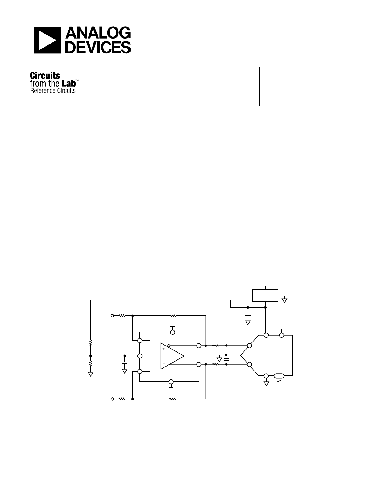
The circuit, shown in Figure 1, uses the ultralow power AD7982
18-bit, 1 MSPS ADC driven by the ADA4940-1, a low power
fully differential amplifier. The ADR395, low noise precision 5.0
V voltage reference is used to supply the 5 V needed for the
ADC. All the ICs shown in Figure 1 are available in small
packages, either 3 mm × 3 mm LFCSP, or 3 mm × 5 mm MSOP,
which helps reduce board cost and space.
Power dissipation of the ADA4940-1 in the circuit is less than
9 mW. The 18-bit, 1 MSPS AD7982 ADC consumes only 7 mW
@ 1 MSPS, which is much lower than competitive ADCs
available in the market. This power also scales with the
throughput. The ADR395 consumes only 0.7mW, making the
total power dissipated by the system less than 17 mW.
CN-0237
Devices Connected/Referenced
ADA4940-1/
ADA4940-2
AD7982 18-Bit, 1 MSPS PulSAR ADC
ADR395
CIRCUIT DESCRIPTION
Modern high resolution SAR ADCs, such as the AD7982 18-bit,
1 MSPS PulSAR® ADC, require a differential driver for optimum
performance. In such applications, the ADC driver takes either
a differential or single-ended signal and performs the level
shifting required to drive the input of the ADC at the right level.
Figure 1 shows the ADA4940-1 differential amplifier level
shifting and driving the 18-bit AD7982 differential input
successive approximation PulSAR ADC. Using four resistors,
the ADA4940-1 can either buffer the signal with a gain = 1 or
amplify the signal for more dynamic range. The ac and dc
performances are compatible with those of the 18-bit, 1 MSPS
AD7982 PulSAR® ADC and other 16- and 18-bit members of
the family, which have sampling rates up to 2 MSPS. This circuit
can also accept a single-ended input signal to generate the same
fully differential output signal.
Single/Dual, Ultralow Power, Low
Distortion Differential ADC Driver
Micropower, Low Noise, Precision 5 V
Bandgap Voltage Reference
Rev.0
Circuits from th
each circuit, and their function and performance have been tested and verified in a lab environ ment at
be liable for direct, indir
whatsoever connected to the use of any Circuits from the Lab circuits. (Continued on last page)
Figure 1. High Performance 18-Bit Differential ADC Driver (Simplified Schematic: All Connections and Decoupling Not Shown)
One Technology Way, P.O. Box 9106, Norwood, MA 02062-9106, U.S.A.
Tel: 781.329.4700
Fax: 781.461.3113 ©2011 Analog Devices, Inc. All rights reserved.
www.analog.com
Page 2

CN-0237 Circuit Note
10144-002
The AD7982 operates on a single VDD supply of 2.5 V. It
contains a low power, high speed, 18-bit sampling ADC and a
versatile serial interface port. The reference voltage (REF) is
applied externally from the ADR395 precision low dropout
(0.3 V) band gap reference, and can be set independently of the
supply voltage. The ADA4940-1 is dc coupled on the input and
the output and performs a differential or single-ended-todifferential conversion if needed. It also buffers the driving
signal. A single-pole 1.8 MHz R-C (33 Ω, 2.7 nF) noise filter is
placed between the op amp output and the ADC input. The
filter also provides some isolation between the op amp output
and the switching spikes at the ADC input due to the internal
sample-and-hold function.
The ADA4940-1 is driven with a 7 V supply (+6 V and –1 V) in
order to provide sufficient headroom on the outputs, which must
swing from 0 V to +5 V for a full-scale input to the ADC.
The gain is set by the ratio of the feedback resistor (R2 = R4) to
the gain resistor (R1 = R3). In addition, the circuit can be used
to convert either single-ended or differential inputs to a differential
output. If needed, a termination resistor in parallel with the
input can be used. Whether the input is a single-ended input or
differential input, the input impedance of the amplifier can be
calculated as show in the MT-076 Tutorial and in the DiffAmpCalc™
Differential Amplifier Calculator (www.analog.com/diffampcalc).
If R1 = R2 = R3 = R4 = 1 kΩ, the single-ended input impedance
is approximately 1.33 kΩ. An external 52.3 Ω termination
resistor provides a 50 Ω termination for the source. An
additional 25.5 Ω (1025.5 Ω total) at the inverting input
balances the parallel impedance of the 50 Ω source and
the termination resistor driving the noninverting input
(52.3 Ω || 50 Ω = 25.5 Ω). Howe ve r, if a differential source input
is used, the differential input impedance is 2 kΩ. In this case, two
52.3 Ω termination resistors are used to terminate each input
if needed.
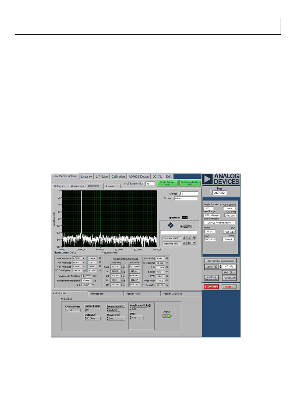
Figure 2. FFT Plot (32,000 Point) for 20 kHz Signal, 0.5 dB Below Full Scale, with Sampling Frequency of 1 MSPS
Rev. 0 | Page 2 of 5
Page 3

Circuit Note CN-0237
10144-003
For the tests on this circuit, the signal generator provided a
10 V p-p differential output. The V
input is bypassed for noise
OCM
reduction and set externally with 1% resistors to maximize the
output dynamic range on the 5 V reference. With an output
common-mode voltage of 2.5 V, each ADA4940-1 output swings
between 0 V and 5 V, opposite in phase, providing a gain of 1
and a 10 V p-p differential signal to the ADC input.
The FFT performance is shown in Figure 2 and is summarized
as follows:
• SNR = 95.06 dBFS (excluding harmonics)
• SINAD = 95.03 dBFS
• SFDR = 105.02 dBFS
• THD = −115.89 dBFS
The INL and DNL performance are shown in Figure 3.
COMMON VARIATIONS
The circuit is proven to work with good stability and accuracy
with component values shown. Other analog-to-digital
converters can be used in place of the AD7982 to achieve the
maximum desired performance. The ADA4940-1/ ADA4940-2
is optimum for driving 16-bit and 18-bit ADCs with minimal
degradation in performance. Faster sampling 18-bit ADCs
include the AD7984 (1.33 MSPS) and AD7986 (2 MSPS).
Differential 16-bit ADCs include the AD7688 (500 kSPS) and
the AD7693 (500 kSPS).
The ADA4940-1/ADA4940-2 rail-to-rail outputs can be driven
to within 0.5 V of each power rail without significant ac
performance degradation. Other differential ADC drivers such
as the AD8137 and ADA4941-1 can also be used to replace the
ADA4940-1 for other applications when speed, input
impedance, or other factors dictate.
CIRCUIT EVALUATION AND TEST
This circuit was tested using a modified E VAL-AD7982SDZ
PulSAR AD7982 evaluation board connected to the converter
evaluation and development board (EVA L-CED1Z).
The AD7982 evaluation board was modified to accept the
ADA4940-1 differential ADC driver and the ADR395 reference.
Figure 3. INL and DNL Plot for 20 kHz Signal, with Sampling Frequency of 1 MSPS
Rev. 0 | Page 3 of 5
Page 4

CN-0237 Circuit Note
PulSAR EV ALUATION BOARD
(MODIF IED EVAL-AD7982S DZ)
PC RUNNING
WINDOW S X P
OR HIGHER
WITH USB P ORT
HIGH SPEED
USB 2.0 CABLE
(INCLUDED)
POWER SUPPLY:
+7.5V DC @ 2A
(INCLUDED)
POWER SUPPLY:
+6V
POWER SUPPLY:
−1V
CONVERTER E V ALUATION AND
DEVELOPMENT BOARD (EVAL-CED1Z)
10144-004
ADR395
POWER
SUPPLY
AGILENT
E3630A
ADA4940-1
EVAL-AD7982SDZ
(MODIFIED)
EVAL-CED1Z
IN+
–1V +6V +7V @ 2A
CED
PC
(USB)
IN–
AUDIO PRECISION
SYS-2702
SIGNAL
GENERATOR
POWER
SUPPLY
ADR395
AD7982
10144-005
The EVA L-AD7982SDZ is a customer evaluation board
intended to ease standalone testing of performance and
functionality for the 18-bit AD7982 PulSAR ADC.
The EVA L-CED1Z board is a platform intended for use in
evaluation, demonstration, and development of systems using
Analog Devices precision converters. It provides the necessary
communications between the converter and the PC,
programming or controlling the device, transmitting or receiving
data over a USB link as shown in Figure 4 and Figure 5.
Equipment Needed
In addition to the two evaluation boards, the external power
supplies of +6 V and –1 V were required for the ADA4940-1.
A "wall wart" supplied the +7.5 V dc voltage for the
EVA L-CED1Z. Other appropriate voltages were supplied to
the AD7982 evaluation board from the EVA L-CED1Z.
Figure 4. PulSAR ADC Evaluation Platform
Figure 5. Test Setup Functional Block Diagram
Rev. 0 | Page 4 of 5
Page 5

Circuit Note CN-0237
A low distortion signal source, the Audio Precision® SYS-2702,
was used to achieve the required performance. A PC with
Windows® XP or Windows 7 equipped with an USB port was
used to run the PulSAR evaluation software.
Getting Started
The software was installed as described at
www.analog.com/EVAL-CED1Z, and
www.analog.com/AD7982_adc_EVAL-CED1Z
The modified AD7982 evaluation board was connected to the
EVA L-CED1Z. The +7.5 V wall wart was connected to the
EVA L-CED1Z. The external power supplies of +6 V and −1 V
were connected to the AD7982 evaluation board.
Setup and Test
An Audio Precision SYS-2702 source was used to provide the
input signal to the AD7982 evaluation board. The PulSAR
evaluation software, which is LabVIEW® based, was used to
control the Audio Precision input signals and also to monitor
the ADC inputs and output.
The software allows the collection and processing of INL, DNL,
and FFT data as shown in Figure 2, Figure 3, and Figure 4.
LEARN MORE
CN-0237 Design Support Package:
www.analog.com/CN0237-DesignSupport
DiffAmpCalc: D
ww
w.analog.com/diffampcalc
Ardizzoni, John. A Practical Guide to High-Speed Printed-
Circuit-Board Layout, Analog Dialogue 39-09, September
2005.
MT-031 Tutorial, Grounding Data Converters and Solving the
Mystery of “AGND” and “DGND”, Analog Devices.
MT-074 Tutorial, Differential Drivers for Precision ADCs,
Analog Devices.
MT-075 Tutorial, Differential Drivers for High Speed ADCs
Overview, Analog Devices.
MT-076 Tutorial, Differential Driver Analysis, Analog Devices.
MT-101 Tutorial, Decoupling Techniques, Analog Devices.
Data Sheets and Evaluation Boards
ADA4940-1 Data Sheet
ADA4940-2 Data Sheet
ADA4940 Evaluation Board
AD7982 Data Sheet
AD7982 Evaluation Board
ADR395 Data Sheet
ifferential Amplifier Calculator:
REVISION HISTORY
10/10—Revision 0: Initial Version
(Continued from first page) Circuits from the L ab circuits are intended only for use with Analog Devices products and are the intellectual property of Analog Devices or its licensors. While you
may use the Circuits from the Lab circuits in the design of your product, no other license is granted by implication or otherwise under any patents or other intellectual property by
application or use of the Circuits from the Lab circuits. Informa tion furnished by Ana log Devices is believed to be accurate and reliable. However, "Circuits from the Lab" are supplied "as is"
and without warranties of any kind, express, implied, or statutory including, but not limited to, any implied warranty of merchantability, noninfringement or fitness for a particular
purpose and no responsibility is assumed by Analog Devices for their use, nor for any infringements of patents or other rights of third parties that may result from their use. Analog Devices
reserves the right to change any Circuits fro m the Lab circuits at any time without notice but is under no obligation to do so.
©2011 Analog Devices, Inc. All rights reserved. Trademarks and
registered trademarks are the property of their respective owners.
CN10144-0-10/11(0)
Rev. 0 | Page 5 of 5
 Loading...