

Page 1
Circuit Note
Rev.0
Circuits from the Lab™ circuits from Analog Devices have been designed and built by Analog Devices
engineers. Standard engineering practices have been employed in the design and construction of
nd their function and performance have been tested and verified in a lab environment at
room temperature. However, you are solely responsible for testing the circuit and determining its
be liable for direct, indirect, special, incidental, consequential or punitive damages due to any cause
whatsoever connected to the use of any Circuits from the Lab circuits. (Continued on last page)
Fax: 781.461.3113 ©2012 Analog Devices, Inc. All rights reserved.
VIN1
VIN0
CB1
10kΩ
10kΩ
34Ω
34Ω
0.1µF
CB6
10kΩ
10kΩ
10kΩ
VIN5
VIN6
VIN6
VIN5
VIN4
VIN3
VIN2
VIN1
VIN0
0.1µF
MASTER
PDhi
CShi
SCLKhi
SDOhi
CNVSThi
SDIhi
ALERThi
PDhi
CShi
SCLKhi
SDOhi
CNVSThi
SDIhi
ALERThi
PDCSSCLK
SDI
CNVST
SDOlo
ALERTlo
1µF
0.1µF
VIN1
VIN0
CB1
V
SS
ALERT
CNVST
PD
SDO
SCLK
SDI
CS
DRIVE
C
REF
V
REF
SDOlo
ALERTlo
AD7280A
AD7280A
AD8280
10kΩ
1kΩ
1kΩ
0.1µF
10kΩ
FERRITE
FERRITE
FERRITE
10kΩ
10kΩ
34Ω
34Ω
0.1µF
10kΩ
0.1µF
10µF
22pF
22pF
22pF
22pF
22pF
22pF
22pF
0.1µF
10µF
V
DD
0
V
DD
0
V
DD
0
V
SS
0
V
DD
1
V
DD
V
DD
VDD1
V
SS
0
V
SS
VIN12
1kΩ
CB6
10kΩ
10kΩ
10kΩ
VIN5
VIN6
0.1µF
0.1µF
VTOPx
TOP
BOT
TESTI
VBOTx
AIOUTOV
AIOUTUV
AIOUTOT
ENBI
VIN11
VIN7
VIN6
VIN5
VIN1
VIN0
VIN12
VIN11
VIN10
VIN9
VIN8
VIN7
VIN6
10kΩ
AVOUTOV
AVOUTUV
ENBI
TESTI
AD8280
10kΩ
TESTO
VTOPx
BOT
TOP
AIINOV
AIINUV
AIINOT
ENBO
VBOTx
10kΩ
22pF
22pF
22pF
22pF
22pF
ADuM1401
V
DD1
GND
1
V
IA
V
IB
V
IC
V
OD
V
DD2
V
DD1
V
DD2
GND
2
GND
1
GND
2
V
DD1
V
ISO
GND
1
GND
ISO
V
OA
V
OB
V
OC
V
ID
V
IA
V
IB
V
IC
V
ID
V
OA
V
OB
V
OC
V
OD
V
OA
V
OB
V
OC
V
OD
V
IA
V
IB
V
IC
V
ID
ADuM1400
ADuM5404
+5V
+3.3V
+3.3V
VIN6
VIN5
VIN4
VIN3
VIN2
VIN1
VIN0
VIN6
VIN5
VIN4
VIN3
VIN2
VIN1
VIN0
10135-001
Circuits from the Lab™ reference circuits are engineered and
tested for quick and easy system integration to help solve today’s
analog, mixed-signal, and RF design challenges. For more
information and/or support, visit www.analog.com/CN0235.
Fully Isolated Lithium Ion Battery Monitoring and Protection System
EVALUATION AND DESIGN SUPPORT
Circuit Evaluation Boards
CN-0235 Circuit Evaluation Board (EVAL-CN0235-SDPZ)
System Demonstration Platform (EVAL-SDP-CB1Z)
Design and Integration Files
Schematics, Layout Files, Bill of Materials
CN-0235
Devices Connected/Referenced
AD7280A Lithium Ion Battery Monitoring System
AD8280 Lithium Ion Battery Safety Monitor
ADuM5404
ADuM1400 Quad-Channel Digital Isolators
CIRCUIT FUNCTION AND BENEFITS
Lithium ion (Li-Ion) battery stacks contain a large number of
individual cells that must be monitored correctly in order to
enhance the battery efficiency, prolong the battery life, and
ensure safety.
Quad-Channel Isolators with
Integrated DC-to-DC Converter
each circuit, a
suitability and applicability for your use and application. Accordingly, in no event shall Analog Devices
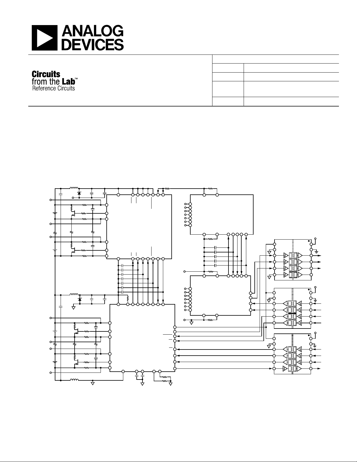
Figure 1. Lithium Ion Battery Monitoring and Protection System Simplified Schematic
One Technology Way, P.O. Box 9106, Norwood, MA 02062-9106, U.S.A.
Tel: 781.329.4700
www.analog.com
Page 2

CN-0235 Circuit Note
The 6-channel AD7280A devices in the circuit shown in
Figure 1 act as the primary monitor providing accurate voltage
measurement data to the System Demonstration Platform
(SDP-B) evaluation board, and the 6-channel AD8280 devices
act as the secondary monitor and protection system. Both
devices can operate from a single wide supply range of 8 V to
30 V and operate over the industrial temperature range of
−40°C to +105°C.
The AD7280A contains an internal ±3 ppm reference that
allows a cell voltage measurement accuracy of ±1.6 mV.
The ADC resolution is 12 bits and allows conversion of up
to 48 cells within 7 μs.
The AD7280A has cell balancing interface outputs designed to
control external FET transistors to allow discharging of
individual cells and forcing all the cells in the stack to have
identical voltages.
The AD8280 functions independently of the primary monitor
and provides alarm functions indicating out of tolerance
conditions. It contains its own reference and LDO, both of
which are powered completely from the battery cell stack. The
reference, in conjunction with external resistor dividers, is used
to establish trip points for the over/undervoltages. Each cell
channel contains programmable deglitching (D/G) circuitry to
avoid alarming from transient input levels.
The AD7280A and AD8280, which reside on the high voltage
side of the battery management system (BMS) have a daisychain interface, which allows up to eight AD7280A’s and e i g ht
AD8280’s to be stacked together and allows for 48 Li-Ion cell
voltages to be monitored. Adjacent AD7280A's and AD8280’s in
the stack can communicate directly, passing data up and down
the stack without the need for isolation.
The master devices on the bottom of the stack use the SPI
interface and GPIOs to communicate with the SDP-B
evaluation board, and it is only at this point that high voltage
galvanic isolation is required to protect the low voltage side of
the SDP-B board. The ADuM1400, ADuM1401 digital isolator,
and the ADuM5404 isolator with integrated dc-to-dc converter
combine to provide the required eleven channels of isolation in
a compact and cost effective solution. The ADuM5404 also
provides isolated 5 V to the VDRIVE input of the lower
AD7280A and the VDD2 supply voltage for the ADuM1400 and
ADuM1401 isolators.
CIRCUIT DESCRIPTION
The AD7280A is a complete data acquisition system that
includes a high voltage input multiplexer, a low voltage input
multiplexe r, a 12-bit, 1 µs SAR ADC, and on-chip registers for
channel sequencing. The HV MUX is used to measure the
series connected Li-Ion battery cells as shown in Figure 1. The
LV MUX provides single-ended ADC inputs that can be used
with external thermistors to measure the temperature of each
battery cell; or, if temperature measurements are not required,
the auxiliary ADC inputs can be used to convert any other 0 V
to 5 V input signal. A precision 2.5 V reference and an on-chip
voltage regulator is also included.
The AD8280 is a hardwire-only safety monitor for lithium ion
battery stacks. In conjunction with the AD7280A, the AD8280
provides a low cost, redundant, battery backup monitor with
adjustable threshold detection and shared or separate alarm
outputs. It has a self-test feature, making it suitable for high
reliability applications, such as automotive hybrid electric
vehicles or higher voltage industrial usage, such as
uninterruptible power supplies. Both the AD7280A and the
AD8280 obtain power from the battery cells they monitor.
The ADuM5404 includes an integrated dc-to-dc converter,
which is used to power the high voltage side of the ADuM1400
and ADuM1401 isolators and provide the VDRIVE supply to
the AD7280A SPI interface. These 4-channel, magnetically
isolated circuits are a safe, reliable, and easy-to-use alternative
to optocouplers.
To optimize the performance of the daisy-chain communication
under noisy conditions, for example, when experiencing
electromagnetic interference, the daisy-chain signals are
shielded on an inner layer of the printed circuit board (PCB).
Shielding is provided above and below by a VSS supply plane,
which is connected to the VSS pin of the upper device in the
chain. Figure 2 shows the top layer of the EVA L-CN0235-SDPZ
PCB, which contains the upper shielding for the AD7280A, and
Figure 5 shows the bottom layer, which contains the upper
shielding for the AD8280. Figure 3 shows the inner layer
(layer 2), which contains the shielded daisy-chain signals, and
the shielding below is carried out on Layer 3 as shown in Figure 4.
Individual 22 pF capacitors are placed on each daisy-chain
connection and are terminated to either the VSS pin of the
upper device or the VDD pin of the lower device, depending on
the direction in which data is flowing on the daisy chain. The
PD, CS, SCLK, SDI, and CNVST daisy-chain connections pass
data up the chain, and the 22 pF capacitors on these pins are
terminated to the VSS of the upper device in the chain.
Rev. 0 | Page 2 of 6
Page 3

Circuit Note CN-0235
10135-002
10135-003
Figure 2. Top Layer of the EVAL-CN0235-SDPZ PCB Contains the Upper Shielding for the Daisy-Chain Signals of the AD7280A
Figure 3. Layer 2 of the EVAL-CN0235-SDPZ PCB Contains the Shielded AD7280A Daisy-Chain Signals
Rev. 0 | Page 3 of 6
Page 4

CN-0235 Circuit Note
10135-004
10135-005
Figure 4. Layer 3 of the EVAL-CN0235-SDPZ PCB Contains the Shielded AD8280 Daisy-Chain Signals
Figure 5. Bottom Layer of the EVAL-CN0235-SDPZ PCB Contains the Upper Shielding for the Daisy-Chain Signals of the AD8280
Rev. 0 | Page 4 of 6
Page 5

Circuit Note CN-0235
531
115
1000
2000
3000
4000
5000
6000
7000
8000
NUMBER OF OCCURANCES
0
9000
2555 2556 2557 2558
CODE
1701
7893
10135-006
246
5019
4016
921
0
1000
2000
3000
4000
5000
6000
2404 2405 2406 2407
NUMBER OF OCCURANCES
CODE
10135-007
The SDOlo and ALERTlo daisy-chain connections pass data
down the chain, and the 22 pF capacitors on these pins are
terminated to the VDD of the lower device in the chain. A direct
low impedance trace is used to connect the VDD of the lower
device with the VSS of the upper device to hold the two
potentials as close as possible together in a noisy environment.
A ground fence at the isolation barrier is used to enclose the low
voltage side, which consists of the left hand side of the PCB.
This fence consists of a guard ring laced together by vias and
connects to the digital ground on all layers throughout the
board. Noise on power and ground planes that reach the edge of
the circuit board can radiate causing emissions, but with this
shielded structure the noise is reflected back.
Input-to-output dipole radiation can also be generated when
driving a current source across a gap between ground planes. To
help minimize this, a continuous shield is used at the isolation
gap whereby the ground planes are extended on all layers
throughout the PCB to create a cross-barrier coupling using
overlapping shields; and the isolation gap on each layer is kept
to a minimum, with a gap of 0.008 inches used on the tested
board. For further recommendations to control radiated
emissions with isoPower® devices, such as the ADuM5404 used
in this circuit, please refer to Application Note AN-0971.
Figure 6. Histogram of Codes for 10,000 Samples, VIN4 – VIN3 of Device 0
Test Results
An important measure of the performance of the circuit is the
amount of noise in the final output voltage measurement.
Figure 6 shows a histogram of 10,000 measurement samples
taken for the VIN3−VIN2 channel. This data was taken
with the CN0235 Evaluation Board connected to the
EVA L -SDP-CB1Z System Demonstration Platform (SDP-B)
evaluation board. Details of the setup are described in the
Circuit Evaluation and Test section of this circuit note.
Twelve Li-Ion batteries were connected to the input screw
terminals. Note that there are only a small percentage of codes
that fall outside the primary bin due to noise. Figure 6 and
Figure 7 show 3 LSBs peak-to-peak noise, corresponding to
approximately 0.5 LSBs rms.
A complete design support package for this circuit note can be
found at www.analog.com/CN0235-DesignSupport.
Figure 7. Histogram for 10,000 Samples, VIN4 - VIN3 of Device 1
COMMON VARIATIONS
The circuit is proven to work with good stability and accuracy.
Other combinations of isolated channels can be used with the
iCoupler isolation products.
CIRCUIT EVALUATION AND TEST
This circuit uses the EVAL-CN0235-SDPZ circuit board and
the EVA L-SDP-CB1Z System Demonstration Platform (SDP-B)
evaluation board. The two boards have 120-pin mating
connectors, allowing for the quick setup and evaluation of the
circuit’s performance. The EVA L -CN0235-SDPZ board contains
the circuit to be evaluated, as described in this note, and the
SDP-B evaluation board is used with the CN0235 evaluation
software to capture the data from the EVA L-CN0235-SDPZ
circuit board.
Rev. 0 | Page 5 of 6
Page 6

CN-0235 Circuit Note
(Continued from first page) Circuits from the L ab circuits are intended only for use with Analog Devices products and are the intellectual property of Analog Devices or its licensors. While you
reserves the right to change any Circuits from the Lab circuits at any time without notice but is under no obligation to do so.
registered trademarks are the property of their respective owners.
Equipment Needed
• PC with a USB port and Windows® XP or Windows Vista®
(32-bit), or Windows® 7 (32-bit)
• EVA L -CN0235-SDPZ circuit evaluation board
• EVA L -SDP-CB1Z SDP-B evaluation board
• CN0235 SDP evaluation software
• Power supply: +6 V, or +6 V “wall wart”
• Li-Ion batteries or precision dc supply
Getting Started
Load the evaluation software by placing the CN0235 Evaluation
Software disc in the CD drive of the PC. Using "My Computer, "
locate the drive that contains the evaluation software.
Functional Block Diagram
See Figure 1 of this circuit note for the circuit block diagram,
and the file “EVAL-CN0235-SDPZ-SCH-RevA.pdf ” for the
circuit schematics. This file is contained in the CN0235 Design
Support Package.
Setup
Connect the 120-pin connector on the E VA L-CN0235-SDPZ
circuit board to the connector marked “CON A” on the
EVA L -SDP-CB1Z evaluation (SDP-B) board. Nylon hardware
should be used to firmly secure the two boards, using the holes
provided at the ends of the 120-pin connectors. With power to
the supply off, connect a +6 V power supply to the pins marked
“+6 V” and “GND” on the board. If available, a +6 V "wall wart"
can be connected to the barrel connector on the board and used
in place of the +6 V power supply. The only other connections
required are to the lithium ion battery stack. The battery stack
can be simulated with a resistor divider, which is driven by a
precision dc supply voltage. Connect the USB cable supplied
with the SDP-B board to the USB port on the PC. Note: Do not
connect the USB cable to the mini USB connector on the SDP-B
board at this time.
Test
Apply power to the +6 V supply (or “wall wart”) connected to
EVA L -CN0235-SDPZ circuit board. Launch the evaluation
software and connect the USB cable from the PC to the USB
mini-connector on the SDP-B board.
Once USB communications are established, the SDP-B board
can be used to send, receive, and capture serial data from the
EVA L -CN0235-SDPZ board.
Information regarding the SDP-B board can be found in the
SDP-B User Guide.
LEARN MORE
CN0235 Design Support Package:
www.analog.com/CN0235-DesignSupport
SDP-B User Guide: www.analog.com/SDP
Ardizzoni, John. A Practical Guide to High-Speed Printed-
Circuit-Board Layout, Analog Dialogue 39-09, September
2005.
MT-031 Tutorial, Grounding Data Converters and Solving the
Mystery of “AGND” and “D GND”, Analog Devices.
MT-101 Tutorial, Decoupling Techniques, Analog Devices.
Data Sheets and Evaluation Boards
CN-0235 Circuit Evaluation Board (EVAL-CN0235-SDPZ)
System Demonstration Platform (EVAL-SDP-CB1Z)
AD7280A Data Sheet and Evaluation Board
AD8280 Data Sheet and Evaluation Board
ADuM5404 Data Sheet
ADuM1400 Data Sheet
REVISION HISTORY
1/12—Revision 0: Initial Version
may use the Circuits from the Lab circuits in the design of your product, no other license is granted by implication or otherwise under any patents or other intellectual property by
application or use of the Circuits from the Lab circuits. Information furnished by Analog Devices is believed to be accurate and reliable. However, "Circuits from the Lab" are supplied "as is"
and without warranties of any kind, express, implied, or statutory including, but not limited to, any implied warranty of merchantability, noninfringement or fitness for a particular
purpose and no responsibility is assumed by Analog Devices for their use, nor for any infringements of patents or other rights of third parties that may result from their use. Analog Devices
©2012 Analog Devices, Inc. All rights reserved. Trademarks and
CN10135-0-1/12(0)
Rev. 0 | Page 6 of 6
 Loading...