

Page 1
Circuit Note
CN-0232
Fractional-N PLL Synthesizer with
Integrated VCO
Rev. 0
the Lab™ circuits from Analog Devices have been designed and built by Analog Devices
engineers. Standard engineering practices have been employed in the design and construction of
room temperature. However, you are solely responsible for testing the circuit and determining its
suitability and applicability for your use and application. Accordingly, in no event shall Analog Devices
irect, special, incidental, consequential or punitive damages due to any cause
whatsoever connected to the use of any Circuits from the Lab circuits. (Continued on last page)
Fax: 781.461.3113 ©2012 Analog Devices, Inc. All rights reserved.
22nF 4.7nF
100nF
360Ω
200Ω
ADF4153
CPGND DGND
CP
1nF1nF
4.7kΩ
R
SET
LE
DATA
CLK
REF
IN
DV
DD
MUXOUT
V
DD
SDV
DD
V
P
100pF
100pF
AV
DD
AGND
ADF4350
V
VCO
V
VCO
V
VCO
V
VCO
DV
DD
AV
DD
V
P
V
TUNE
CP
OUT
PDB
RF
SDV
DD
RF
OUT
B+
RF
OUT
B–
RF
OUT
A–
RF
OUT
A+
CE
V
DD
CPGND AGND DGND
4.7kΩ
R
SET
LE
DATA
CLK
REF
IN
MUXOUT
LOCK
DETECT
51Ω
A
GNDVCO
LD
SD
GND
TEMP V
REF
V
COM
SW
10pF 0.1µF
1nF
1nF
1nF
1nF
TCXO
26MHz
51Ω
51Ω
51Ω
51Ω
51Ω
51Ω 51Ω
RFOUTA+
VCO
COUNTERS
PHASE
FREQUENCY
DETECTOR
CHARGE
PUMP
COUNTERS
PHASE
FREQUENCY
DETECTOR
CHARGE
PUMP
RFOUTB+
VCO
TUNING
VOLTAGE
REFERENCE
LOOP FILTER
RF IN
3.3V
3.3V
3.3V
51Ω
10pF 0.1µF
10pF 0.1µF
1nF1nF
8
11
12
13
1
2
3
1
29
SPI COMPAT IBLE SERIAL BUS
RFINA
RF
IN
B
15
3
4
9
6
5
14
7
2
16 10
10
28
16
8 31 9 11 18 21 27
14
15
19 23 24
25
30
17
20
7
26
6 32
5
4
12
13
22
SPI COMPAT IBLE SERIAL BUS
10125-001
Circuits from the Lab™ reference circuits are engineered and
tested for quick and easy system integration to help solve today’s
analog, mixed-signal, and RF design challenges. For more
information and/or support, visit www.analog.com/CN0232.
Devices Connected/Referenced
ADF4350
ADF4153 Fractional-N PLL Frequency Synthesizer
Minimizing Spurious Outputs Using a Synthesizer with an Integrated VCO and
an External PLL Circuit
EVALUATION AND DESIGN SUPPORT
Circuit Evaluation Boards
ADF4350 Evaluation Board (EVAL-ADF4350EB2Z)
ADF4153 Evaluation Board (EVAL-ADF4153EBZ1)
Design and Integration Files
Schematics, Layout Files, Bill of Materials
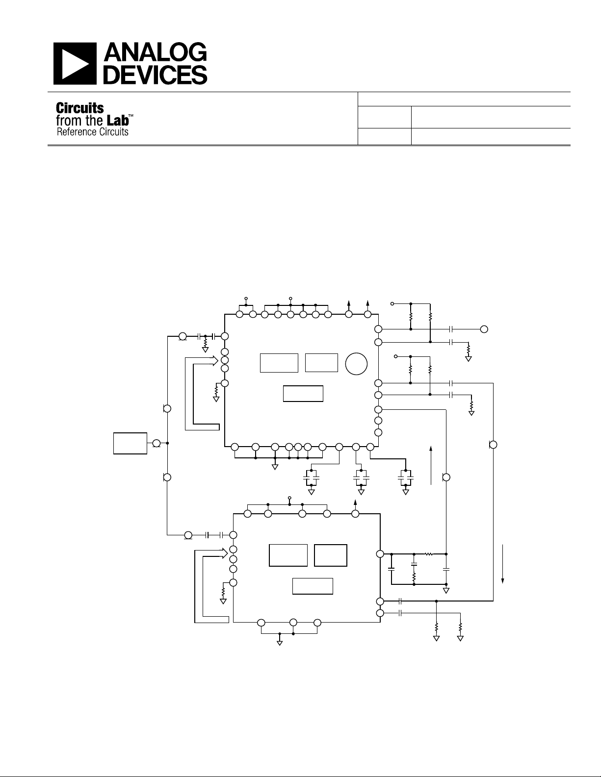
CIRCUIT FUNCTION AND BENEFITS
The circuit shown in Figure 1 uses the ADF4350 synthesizer with
an integrated VCO and an external PLL to minimize spurious
outputs by isolating the PLL synthesizer circuitry from the VCO
circuit.
Figure 1. ADF4153 PLL Connected to ADF4350 (Simplified Schematic: All Connections and Decoupling Not Shown)
Circuits from
each circuit, and their function and performance have been tested and verified in a lab environment at
be liable for direct, ind
One Technology Way, P.O. Box 9106, Norwood, MA 02062-9106, U.S.A.
Tel: 781.329.4700
www.analog.com
Page 2

CN-0232 Circuit Note
Devices with integrated PLLs and VCOs may have feed through
from the digital PLL circuitry to the VCO, leading to higher
spurious levels due to the close proximity of the PLL circuitry
to the VCO.
The circuit shown in Figure 1 uses the ADF4350, a fully integrated
fractional-N PLL and VCO that can generate frequencies from
137.5 MHz to 4400 MHz, together with the ADF4153 PLL.
In addition to improvements in spurious performance,
another possible advantage of using an external PLL is the
possibility of increased frequency resolution. For example,
if the ADF4157 PLL is selected in place of the ADF4153, the
frequency resolution of the PLL can be as fine as 0.7 Hz.
CIRCUIT DESCRIPTION
The ADF4350 is a wideband PLL and VCO consisting of
three separate multiband VCOs. Each VCO covers a range of
approximately 700 MHz (with some overlap between the
frequencies of the VCO). This permits a fundamental VCO
frequency range of between 2.2 GHz to 4.4 GHz. Frequencies
lower than 2.2 GHz can be generated using internal dividers
within the ADF4350.
For most applications, the internal PLL of the ADF4350 is used to
lock the VCO. In addition to locking the PLL, the PLL circuitry
performs an additional vital function of VCO band select, using
the internal reference (R) and feedback (N) counters of the internal
PLL to compare the VCO output with the reference input.
For frequency generation, the internal PLL must be enabled and
the desired frequency must be programmed. Then, once sufficient
time has elapsed for band select, the internal PLL can be disabled,
and, finally, the external PLL can be enabled. The external PLL
compares the reference frequency and the VCO output frequency
to generate a stable dc voltage to lock the PLL.
Figure 2 shows the output frequency spurs measured at RF
OUT
A+
using the ADF4350 internal PLL and VCO with the ADF4153 PLL
disabled. Note the presence of PFD spurs at 13 MHz and 26 MHz.
Figure 3 shows the output spurs measured at RF
A+ with the
OUT
ADF4350 internal PLL circuit disabled and the external ADF4153
PLL active. In this mode, the charge pump output of the ADF4153
drives the loop filter, which in turn drives the V
ADF4350. The V
input controls the ADF4350 VCO output
TUNE
input of the
TUNE
fre quency.
In making a comparison between Figure 2 and Figure 3, the spurs
due to the phase frequency detector (PFD) frequency, at 13 MHz
and 26 MHz, in Figure 2 have disappeared into the noise floor
in Figure 3.
COMMON VARIATIONS
Different PLLs can be selected. The fractional-N PLL in both the
ADF4350 and ADF4153 has a minimum frequency resolution
of PFD/4095. If finer resolution is required, the ADF4157
can be selected. The resolution of this PLL is PFD/2
providing an ultrafine resolution of <1 Hz.
For applications requiring simpler software programmability,
the ADF4150 PLL is software compatible with the ADF4350,
easing the software programming sequence.
25
, thereby
Rev. 0 | Page 2 of 6
Page 3

Circuit Note CN-0232
R&S FSUP SI GNAL SOURCE ANALY ZER
SETTINGS
RESIDUAL NO ISE
(T1 WITHOUT SPURS) SPUR LIST
SIGNAL FREQUENCY: 1.6000GHz INT PHN (1.0k .. 30.0M) : –49.1dBc
SIGNAL LEVEL: 5.44dBm RESIDUAL PM : 0.285°
CROSS CORR MODE: HARMONIC 1 RESIDUAL F M : 3.24kHz
INTERNAL RE F TUNED: INTERNAL PHAS E DE T RMS JITTER: 0.4946ps
1.000MHz –83.82dBc
2.001MHz –99.68dBc
3.000MHz –89.92dBc
13.000MHz –94.70dBc
PHASE NOISE (dBc/Hz) MARKER 1 (T1) MARKER 2 (T1) MARKER 3 (T1) MARKE R 4 ( T1)
RF ATTEN: 5dB 1kHz 10.98633kHz 13.00011MHz 26.00002MHz
TOP –70dBc/Hz –91.84dBc/Hz –93.42dBc/Hz –94.7dBc –87.89dBc
10k 100k 1M 10M1k 30M
–160
–170
–150
–140
–130
–120
–110
–100
–90
–80
–70
SPUR POWE R ( dBc)
FREQUENCY OFFSET (Hz)
4
1
2
3
SPR OFF
TH 0dB
LOOP BW 300Hz
10125-002
R&S FSUP SI GNAL SOURCE ANALY ZER
SETTINGS
RESIDUAL NO ISE
(T1 WITHOUT SPURS) SPUR LIST
SIGNAL FREQUENCY: 1.6000GHz INT PHN (1.0k .. 30.0M) : –53.3dBc
SIGNAL LEVEL: 1.71dBm RESIDUAL PM : 0.174°
CROSS CORR MODE: HARMONIC 1 RESIDUAL F M : 1.846kHz
INTERNAL RE F TUNED: INTERNAL PHAS E DE T RMS JITTER: 0.3025ps
1000.0kHz –90.44dBc
2.000MHz –85.60dBc
3.000MHz –96.36dBc
4.000MHz –99.28dBc
PHASE NOISE (dBc/Hz) MARKER 1 (T1) MARKER 2 (T1) MARKER 3 (T1) MARKE R 4 ( T1)
RF ATTEN: 5dB 1kHz 1kHz 100kHz 1MHz
TOP –70dBc/Hz –101.23dBc/Hz –101.23dBc/Hz –120.62dBc –144.68dBc
10k 100k 1M 10M1k 30M
–160
–170
–150
–140
–130
–120
–110
–100
–90
–80
–70
SPUR POWE R ( dBc)
FREQUENCY OFFSET (Hz)
1
2
3
SPR OFF
TH 0dB
LOOP BW 300Hz
10125-003
4
Figure 2. ADF4350 PFD Spurs at 1.6 GHz
Figure 3. ADF4350 PFD Spurs at 1.6 GHz Using ADF4153 PLL
Rev. 0 | Page 3 of 6
Page 4

CN-0232 Circuit Note
REFERENCE
FREQUENCY
GENERATOR
(R&S SMA100A)
SPECTRUM
ANALYZER
(R&S FSUP26)
9V BATTERY
POWER
SUPPLY
50Ω
TERM
50Ω
TERM
RFOUTA+
RFOUTA−
RFOUTB+
RFIN+
CP OUT
VTUNE
PC
PC
USB
PRINTER
COM5.5V
J14 J15
J4
ADF4350
EVALUATI ON BOARD
(EVAL-ADF4350EB2Z)
J2
J3
RFOUTB−
J5
J1
T4
T7
ADF4153
EVALUATI ON BOARD
(EVAL-ADF4153EBZ1)
J5
J2
EVAL-
ADF4xxxX-USB
USB
10125-004
CIRCUIT EVALUATION AND TEST
The CN-0232 uses the EVAL-ADF4350EB2Z board for
evaluation of the described circuit, and with some minor
modifications, allows for quick setup and evaluation. The
EVAL-ADF4350EB2Z board uses the standard ADF4350
programming software, contained on the CD that accompanies
the evaluation board. The EVA L -ADF4153EBZ1 evaluation
board comes with the software for the ADF4153 PLL.
Equipment Needed
• EVA L -ADF4350EB2Z with programming software.
• EVA L -ADF4153EBZ1 with programming software.
• 5.5 V power supply.
• R&S SMA100A signal generator or equivalent.
• R&S FSUP26 spectrum analyzer or equivalent.
• Two PCs with Windows® XP, Windows, Vista (32-bit), or
Windows 7 (32-bit), one with an USB port and the other
with a printer port. Alternatively, the EVAL-ADF4xxxXUSB USB adaptor kit can be used instead of the printer
port, if none is available.
The SMA coaxial cable is required to connect RFOUTB+ of the
EVA L -ADF4350EB2Z to RFIN of the E VA L-ADF4153EBZ1. A
simple SMA splitter is also needed to share the reference source
between the two boards. Some flexible microcoaxial cable is
required to connect the output of the ADF4153 loop filter to the
ADF4350 V
sides of the cable must be grounded to suitable GND points on
each board.
input. To minimize unwanted interference, both
TUNE
Functional Block Diagram
For this experiment, the E VA L-ADF4153EBZ1 and the EVA L-
ADF4350EB2Z are used. The EVA L-ADF4350EB2Z is selected
because it contains the auxiliary RFOUTB+ output stage, which is
connected via SMA cable to the EVA L -ADF4153EBZ1, as shown
in Figure 4.
Both PLLs use the same reference input (REFIN) frequency;
therefore, an SMA splitter connects the same REFIN to both
boards.
The loop filter output on the E VA L-ADF4153EBZ1 is connected
to the V
pin of the ADF4350 via a shielded coaxial cable to
TUNE
ensure that no extra noise or spurs appear on the pin. Both
parts are programmed separately. It may be necessary to use
different PCs for each board to ensure no conflicts occur
between hardware drivers.
Getting Started
The UG-110 user guide details the installation and use of the
EVA L -ADF4350EB2Z evaluation software. UG-110 also
contains board setup instructions and the board schematic,
layout, and bill of materials.
The UG-167 user guide contains similar information relevant to
the EVA L -ADF4153EBZ1. Necessary modifications to the board
are the removal of the VCO (Y1). To reconfigure this board as
an input, remove the R7 resistor and change R8 and R9 to 0 Ω.
The PLL loop filter on the ADF4350 board is unused and
should be removed. At this point, the microcoaxial cable can be
used to connect the output of the ADF4153 loop filter (T7) to
the V
pin of the ADF4350 (T4). It is of critical importance
TUNE
that the outer shielding of this cable is connected to a ground
point on both boards.
Figure 4. Test Setup Functional Diagram
Rev. 0 | Page 4 of 6
Page 5

Circuit Note CN-0232
10125-006
Initialization Procedure
The ADF4350 must go through the band select process for every
new frequency.
1. Initialize the ADF4350 as normal (program R5, R4, R3, R2,
R1, R0), except set DB4, R2 to 1 (I
because the ADF4350 charge pump is unused. Set DB9, R4 to
0 for divided VCO output on RFOUTB+. Enable RFOUTB+
(auxiliary out). This signal is fed to the ADF4153 over the
coax cable.
2. Initialize the ADF4153 (as per the data sheet) to accept the
VCO output frequency as the RF input frequency. Note
that the band select switch is internal; therefore, an external
switch to remove the PLL V
TUNE
3. When the ADF4153 achieves lock, the ADF4350 counter
reset to 1 (DB3, R2) must be activated. Not activating the
counter reset degrades spur performance. Additionally, all
ADF4350 synthesizer blocks can be powered down using
the test mode bit (DB10, R5).
three-state enabled),
CP
is not required.
Frequency Update
1. Program DB10, R5 to 0 to reactivate the ADF4350 synthesizer
blocks.
2. Program DB3, R2 of the ADF4350 to 0 to deactivate the
counter reset because these counters are required for band
select.
3. Program the ADF4350 and ADF4153 N-counter registers
as appropriate for the new frequency.
4. When the ADF4153 achieves lock, the ADF4350 counter
reset (DB3, R2) can be activated. Additionally all synthesizer
blocks can be powered down using the test mode bit
(DB10, R5).
5. Repeat Step 1 to Step 4 as required for new frequencies.
The software screen captures shown in Figure 5 and Figure 6 show
the software windows for 26 MHz REF
(ADF4350) and 13 MHz
IN
PFD (ADF4153).
After setting up the equipment, use standard RF test methods to
measure the spectral purity of the output signal.
10125-005
Figure 5. ADF4350 Software Window
Figure 6. ADF4153 Software Window
Rev. 0 | Page 5 of 6
Page 6

CN-0232 Circuit Note
(Continued from first page) Circuits from the Lab circuits are intended only for use with Analog Devices products and are the intellectual property of Analog Devices or its licensors. While you
reserves the right to change any Circuits from the Lab circuits at any time without notice but is under no obligation to do so.
LEARN MORE
CN0232 Design Support Package:
http://www.analog.com/CN0232-DesignSupport
UG-110, User Guide for the EVAL-ADF4350EB2Z board
UG-167, User Guide for the EVAL-ADF4153EBZ1 board
MT-031 Tutorial, Grounding Data Converters and Solving the
Mystery of “AGND” and “DGND”, Analog Devices.
MT-086 Tutorial, Fundamentals of Phase Locked Loops (PLLs),
Analog Devices.
MT-101 Tutorial, Decoupling Techniques, Analog Devices.
ADIsimPLL Design Tool
Data Sheets and Evaluation Boards
ADF4350 Evaluation Board (EVA L -ADF4350EB2Z)
ADF4153 Evaluation Board (EVA L -ADF4153EBZ1)
ADF4153 Data Sheet
ADF4350 Data Sheet
REVISION HISTORY
4/12—Revision 0: Initial Version
may use the Circuits from the Lab circuits in the design of your product, no other license is granted by implication or otherwise under any patents or other intellectual property by
application or use of the Circuits from the Lab circuits. Information furnished by Analog Devices is believed to be accurate and reliable. However, Circuits from the Lab circuits are supplied
"as is" and without warranties of any kind, express, implied, or statutory including, but not limited to, any implied warranty of merchantability, noninfringement or fitness for a particular
purpose and no responsibility is assumed by Analog Devices for their use, nor for any infringements of patents or other rights of third parties that may result from their use. Analog Devices
©2012 Analog Devices, Inc. All rights reserved. Trademarks and
registered trademarks are the property of their respective owners.
CN10125-0-4/12(0)
Rev. 0 | Page 6 of 6
 Loading...