

Page 1
Circuit Note
Devices Connected/Referenced
Circuits from the Lab™ reference circuits are engineered and
tested for quick and easy system integration to help solve today’s
analog, mixed-signal, and RF design challenges. For more
information and/or support, visit www.analog.com/CN0217.
AD5933
AD5934
1 MSPS, 12-Bit Impedance Converter,
Network Analyzer
250kSPS, 12-Bit Impedance Converter,
Network Analyzer
AD8606 Precision Low Noise Dual CMOS Op Amp
High Accuracy Impedance Measurements Using 12-Bit Impedance Converters
EVALUATION AND DESIGN SUPPORT
Circuit Evaluation Boards
CN-0217 Circuit Evaluation Board
(EVAL-CN0217-EB1Z)
Design and Integration Files
Schematics, Layout Files, Bill of Materials
SCL
SDA
MCLK
OSCILLATOR
I2C
INTERFACE
REAL
REGISTER
IMAGINARY
REGISTER
1024-POINT DFT
AGND DGND
V
DD
ADC
(12 BITS)
V
DD
DVDDAVDD
DDS
CORE
(27 BITS)
TEMPERATURE
SENSOR
AD5933/AD5934
LPF
DAC
OUTPUT AMPLIFIER
GAIN
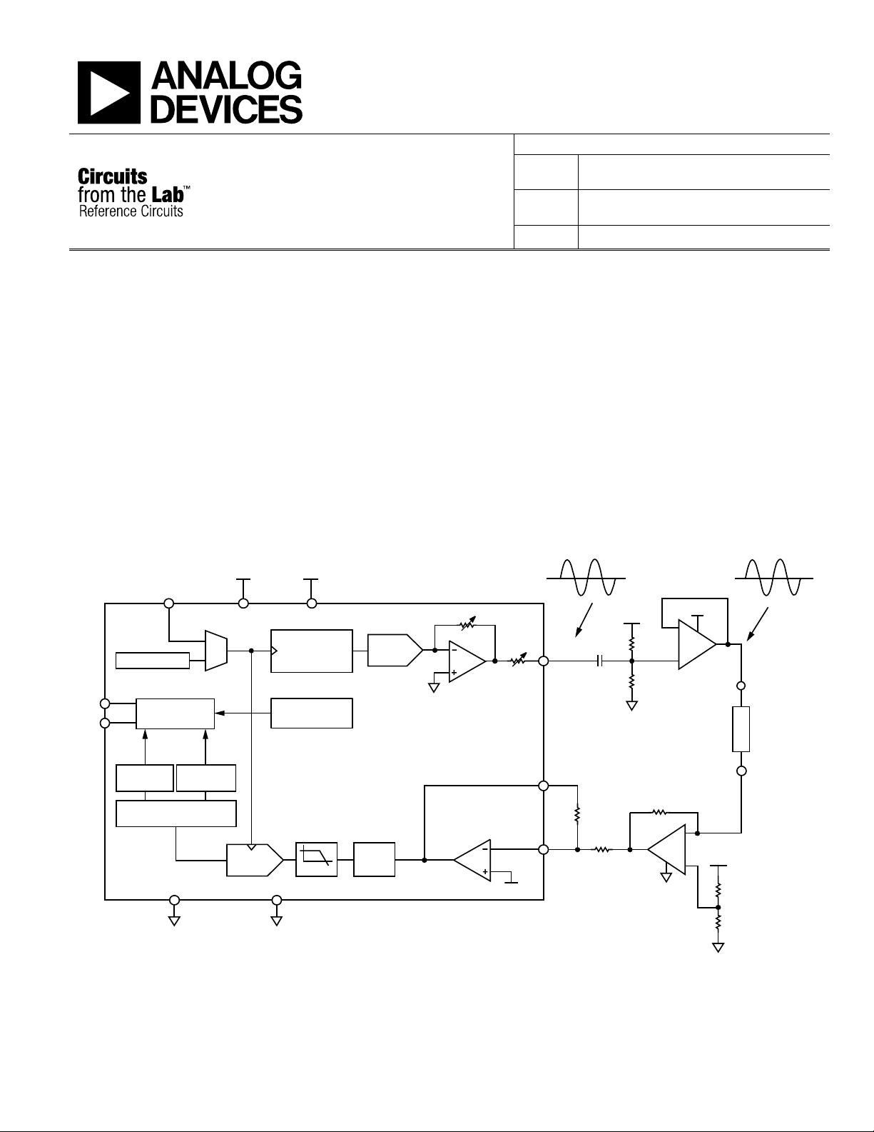
CIRCUIT FUNCTION AND BENEFITS
The AD5933 and AD5934 are high precision impedance
converter system solutions that combine an on-chip
programmable frequency generator with a 12-bit, 1 MSPS
(AD5933) or 250 kSPS (AD5934) analog-to-digital converter
(ADC). The tunable frequency generator allows an external
complex impedance to be excited with a known frequency.
The circuit shown in Figure 1 yields accurate impedance
measurements extending from the low ohm range to several
hundred kΩ and also optimizes the overall accuracy of the
AD5933/AD5934.
1.98V p-p
TRANSMIT S IDE
I-V
R
OUT
VDD/2
1.48V
VOUT
RFB
VIN
47nF
20kΩ
20kΩ
V
DD
50kΩ
50kΩ
A1, A2 ARE
½
AD8606
R
FB
A2
VDD/2
V
DD
−
A1
+
−
V
+
DD
50kΩ
50kΩ
CN-0217
1.98V p-p
Z
UNKNOWN
Figure 1. Optimized Signal Chain for Impedance Measurement Accuracy (Simplified Schematic, All Connections and Decoupling Not Shown)
Rev.0
Circuits from the Lab™ circuits from Analog Devices have been designed and built by Analog Devices
engineers. Standard engineering practices have been employed in the design and construction of
each circuit, and their function and performance have been tested and verified in a lab environment at
room temperature. However, you are solely responsible for testing the circuit and determining its
suitability and applicability for your use and application. Accordingly, in no event shall Analog Devices
be liable for direct, indirect, special, incidental, consequential or punitive damages due to any cause
w
atsoever connected to the use of any Circuits from the Lab circuits. (Continued on last page)
h
One Technology Way, P.O. Box 9106, Norwood, MA 02062-9106, U.S.A.
Tel: 781.329.4700
Fax: 781.461.3113 ©2
011 Analog Devices, Inc. All rights reserved.
www.analog.com
09915-001
Page 2
FREQUENCY (Hz)
100
90
0
1k
100M10k 100k 1M 10M
80
70
20
60
50
30
10
40
A
V
= 100
AV = 10
AV = 1
VS = 2.7V
09915-002
OUTPUT IMPEDANCE (Ω)
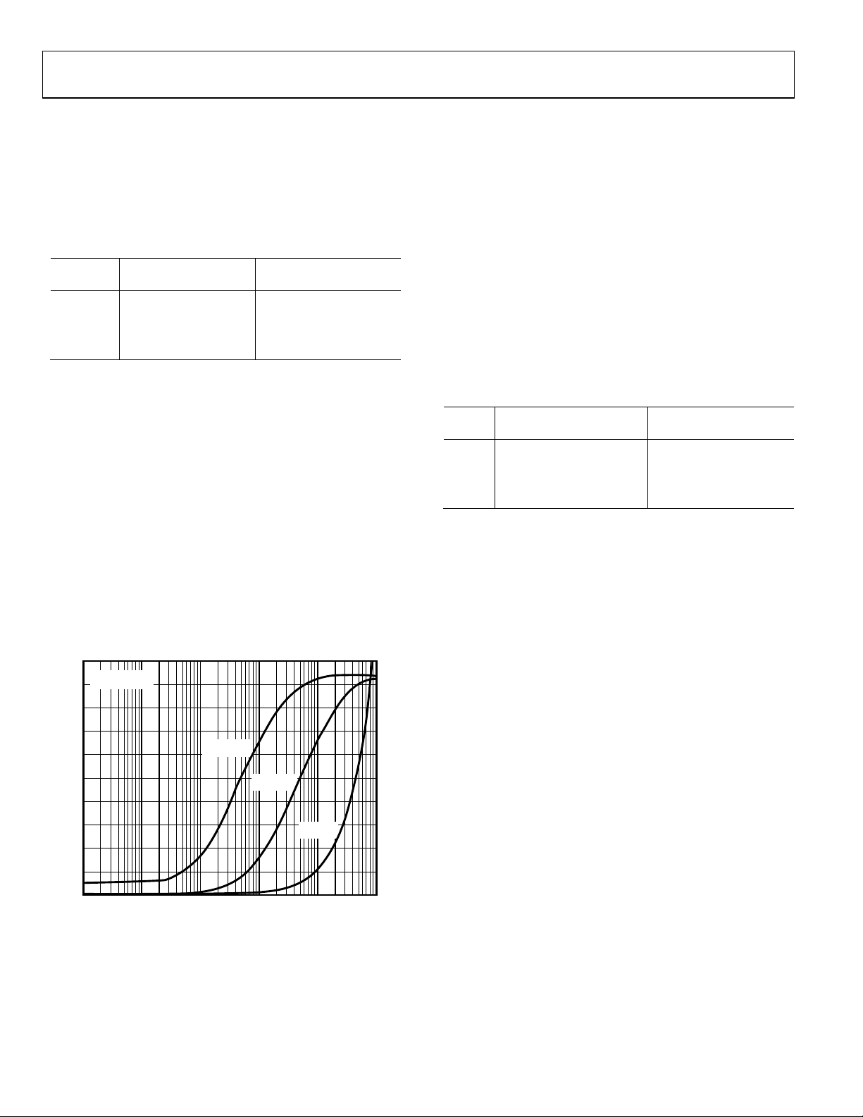
CN-0217 Circuit Note
CIRCUIT DESCRIPTION
The AD5933 and AD5934 have four programmable output
voltage ranges; each range has an output impedance associated
with it. For example, the output impedance for a 1.98 V p-p
output voltage is typically 200 Ω (see Table 1).
Table 1. Output Series Resistance, R
for VDD = 3.3 V Supply Voltage,
Output Excitation
Range
Amplitude
Range 1 1.98 V p-p 200 Ω typ
Range 2 0.97 V p-p 2.4 kΩ typ
Range 3 0.383 V p-p 1.0 kΩ typ
Range 4 0.198 V p-p 600 Ω typ
This output impedance impacts the impedance measurement
accuracy, particularly in the low kΩ range, and should be taken
into account when calculating the gain factor. Please refer to the
AD5933 or AD5934 data sheets for more details on gain factor
calculation.
A simple buffer in the signal chain prevents the output
impedance from affecting the unknown impedance
measurement. A low output impedance amplifier should be
selected with sufficient bandwidth to accommodate the
AD5933/AD5934 excitation frequency. An example of the low
output impedance achievable is shown in Figure 2 for the
AD8605/AD8606/AD8608 family of CMOS op amps. The
output impedance for this amplifier for an A
1 Ω up to 100 kHz, which is the maximum operating range of the
AD5933/AD5934.
Figure 2. Output Impedance of AD8605/AD8606/AD8608
, vs. Excitation Range
OUT
Output Resistance,
R
OUT
of 1 is less than
V
Rev. 0 | Page 2 of 6
Matching the DC Bias of Transmit Stage to Receive Stage
The four programmable output voltage ranges in the AD5933/
AD5934 have four associated bias voltages (Table 2). For
example, the 1.98 V p-p excitation voltage has a bias of 1.48 V.
However, the current-to-voltage (I-V) receive stage of the
AD5933/AD5934 is set to a fixed bias of VDD/2 as shown in
Figure 1. Thus, for a 3.3 V supply, the transmit bias voltage is
1.48 V, while the receive bias voltage is 3.3 V/2 = 1.65 V. This
potential difference polarizes the impedance under test and can
cause inaccuracies in the impedance measurement.
One solution is to add a simple high-pass filter with a corner
frequency in the low Hz range. Removing the dc bias from the
transmit stage and re-biasing the ac signal to VDD/2 keeps the
dc level constant throughout the signal chain.
Table 2. Output Levels and Respective DC Bias for VDD =
3.3 V Supply Voltage
Output Excitation
Range
Amplitude Output DC Bias Level
1 1.98 V p-p 1.48 V
2 0.97 V p-p 0.76 V
3 0.383V p-p 0.31 V
4 0.198 V p-p 0.173 V
Selecting an Optimized I-V Buffer for the Receive Stage
The current-to-voltage (I-V) amplifier stage of the
AD5933/AD5934 can also add minor inaccuracies to the signal
chain. The I-V conversion stage is sensitive to the amplifier's
bias current, offset voltage, and CMRR. By selecting the proper
external discrete amplifier to perform the I-V conversion, the
user can choose an amplifier with lower bias current and offset
voltage specifications along with excellent CMRR, making the
I-V conversion more accurate. The internal amplifier can then
be configured as a simple inverting gain stage.
Selection of resistor R
still depends on the gain through the
FB
system as described in the AD5933/AD5934 data sheet.
Optimized Signal Chain for High Accuracy Impedance Measurements
Figure 1 shows a proposed configuration for measuring low
impedance sensors. The ac signal is high-pass filtered and rebiased before buffering with a very low output impedance
amplifier. The I-V conversion is completed externally before the
signal returns to the AD5933/AD5934 receive stage. Key
specifications that determine the required buffer are very low
output impedance, single-supply capability, low bias current,
low offset voltage, and excellent CMRR performance. Some
suggested parts are the AD4528-1, AD8628/AD8629, AD8605,
and AD8606. Depending on board layout, use a single-channel
or dual-channel amplifier. Use precision 0.1% resistors for both
the biasing resistors (50 kΩ) and gain resistors (20 kΩ and R
to reduce inaccuracies.
)
FB
Page 3

Circuit Note CN-0217
35
30
25
20
15
10
5
0
29.95 30.00 30.05 30.10 30.15 30.20
10.3Ω
30Ω
1µF
30.25
FREQUENCY ( kHz )
MAGNITUDE (Ω)
09915-003
20
0
–20
–40
–60
–80
–100
29.95 30.00 30.05 30.10 30.15 30.20
1µF
30.25
FREQUENCY ( kHz )
PHASE (Degrees)
09915-004
10.3Ω, 30Ω
10.22
10.20
10.18
10.16
10.14
10.12
10.10
10.08
10.06
10.04
29.50 30.00 30.05 30.10 30.15 30.20 30.25
FREQUENCY ( kHz )
MAGNITUDE (Ω)
09915-005
CIRCUIT EVALUATION AND TEST
The schematic in Figure 1 was developed to improve impedance
measurement accuracy, and some example measurements were
taken. The AD8606 dual channel amplifier buffers the signal on
the transmit path and converts the receive signal from current
to voltage. For the three examples shown, the gain factor is
calculated for each frequency increment to remove frequency
dependent errors. A complete design package including schematics, bill of materials, layout, and Gerber files is available for this
solution at http://www.analog.com/CN0217-DesignSupport.
The software used is the same software that is available with
evaluation boards and is accessible from the AD5933 and
AD5934 product pages.
Example 1: Low Impedance Range
Table 1. Low Impedance Range Setup for VDD = 3.3 V
Supply Voltage
Parameter Value
V p-p 1.98 V (Range 1)
Number of Settling Time Cycles 15
MCLK 16 MHz
R
20.1 Ω
CAL
RFB 20.0 Ω
Excitation Frequency Range 30 kHz to 30.2 kHz
Unknown Impedances R1 = 10.3 Ω,
R2 = 30.0 Ω,
C3 = 1 µF (Z
30 kHz)
The results of the low impedance measurements are shown in
Figure 3, Figure 4, and Figure 5. Figure 5 is for the 10.3 Ω
measurement and is shown on an expanded vertical scale.
The accuracy achieved is very much dependent on how large
the unknown impedance range is relative to the calibration
resistor, R
impedance of 10.3 Ω measured 10.13 Ω, an approximate 2%
error. Choosing an R
achieves a more accurate measurement; that is, the smaller the
unknown impedance range is centered around R
accurate the measurement. Consequently, for large unknown
impedance ranges, it is possible to switch in various R
resistors to break up the unknown impedance range using
external switches. The R
calibration during the R
switch to select various R
range of the signal seen by the ADC.
Also note that to achieve a wider range of measurements a
200 mV p-p range was used. If the unknown Z is a small range,
a larger output voltage range can be used to optimize the ADC
dynamic range.
. Therefore, in this example, the unknown
CAL
closer to the unknown impedance
CAL
error of the switch is removed by
ON
gain factor calculation. Using a
CAL
values can optimize the dynamic
FB
= 5.3 Ω at
C
is, the more
CAL
CAL
Figure 3. Measured Low Impedance Magnitude Results
Figure 4. Measured Low Impedance Phase Results
Figure 5. Measured 10.3 Ω Magnitude Results (Expanded Scale)
Rev. 0 | Page 3 of 6
Page 4

CN-0217 Circuit Note
60
70
80
90
100
110
120
30 35 40
FREQUENCY (kHz)
IMPEDANCE MAGNITUDE (kΩ)
45 50
MEASURED
IDEAL
09915-006
–90.3
–90.2
–90.1
–90.0
–89.9
–89.8
–89.7
–89.6
–89.5
–89.4
–89.3
30 35 40
FREQUENCY (kHz)
PHASE (Degrees)
45 50
09915-007
30 35 40
FREQUENCY (kHz)
45 50
8160
8180
8200
8220
8240
8260
8280
IMPEDANCE MAGNITUDE (Ω)
R3
IDEAL
09915-008
30 35 40
FREQUENCY (kHz)
45 50
IMPEDANCE MAGNITUDE (kΩ)
R4
09915-009
213.5
214.0
214.5
21.50
215.5
216.0
216.5
217.0
217.5
218.0
218.5
IDEAL
Example 2: kΩ Impedance Range
Using an R
ances were measured according to the setup conditions listed
in Table 2. Figure 6 to Figure 10 document accuracy results.
To improve the overall accuracy, select an R
the unknown impedance. For example, in Figure 9, an R
closer to the Z
impedance range is large, use more than one R
Table 2. kΩ Impedance Range Setup for VDD = 3.3 V Supply
Voltage
Parameter Value
V p-p 0.198 V (Range 4)
Number of Settling Time Cycles 15
MCLK 16 MHz
R
99.85 kΩ
CAL
RFB 100 kΩ
Excitation Frequency Range 30 kHz to 50 kHz
Unknown Impedances R0 = 99.85 kΩ
of 99.85 kΩ, a wide range of unknown imped-
CAL
value closer to
CAL
value of 217.5 kΩ is required. If the unknown
C
resistor.
CAL
R1 = 29.88 kΩ
R2 = 14.95 kΩ
R3 = 8.21 kΩ
R4 = 217.25 kΩ
C5 = 150 pF (ZC = 26.5 kΩ at
40 kHz)
C6 = 47pF (Z
= 84.6 kΩ at
C
40 kHz)
CAL
Figure 7. Phase Result for ZC = 47 pF, R
= 99.85 kΩ
CAL
Figure 6. Magnitude Result for Z
= 47 pF, R
C
CAL
= 99.85 kΩ
Rev. 0 | Page 4 of 6
Figure 8. Z
Figure 9. Z
= 8.21 kΩ, R
C
= 217.25 kΩ, R
C
= 99.85 kΩ
CAL
= 99.85 kΩ
CAL
Page 5

Circuit Note CN-0217
0
20
40
60
80
100
120
30 32 34 36 38 40 42 44 46 48 50
IMPEDANCE MAGNITUDE (kΩ)
FREQUENCY (kHz)
R1
R3
C5
R0
C6
R2
09915-010
500
0
1000
1500
2000
2500
3000
3500
4000
4 24 44 64 84 104
IMPEDANCE MAGNITUDE (Ω)
FREQUENCY (kHz)
IDEAL
MEASURED
09915-011
4 24 44 64 84 104
FREQUENCY (kHz)
IDEAL
MEASURED
09915–012
–95
–90
–85
–80
–75
–70
–65
–60
PHASE (Degrees)
Figure 10. Magnitude Results for Example 2: R1, R2, R3, C5, C6
Example 3: Parallel R-C (R||C) Measurement
An R||C type measurement was also made using the
configuration, using an R
of 1 kΩ, an R of 10 kΩ, and a C of
CAL
10 nF, measured across a frequency range of 4 kHz to 100 kHz.
The magnitude and phase results versus ideal are plotted in
Figure 11 and Figure 12.
Table 3. R||C Impedance Range Setup for VDD = 3.3 V
Supply Voltage
Parameter Value
V p-p 0.383 V (Range 3)
Number of Settling Time Cycles 15
MCLK 16 MHz
R
1 kΩ
CAL
RFB 1 kΩ
Excitation Frequency Range 4 kHz to 100 kHz
Unknown Impedance R||C R = 10 kΩ
C = 10 nF
Figure 11. Magnitude Results for ZC = 10 kΩ||10 nF, R
= 1 kΩ
CAL
Setup and Test
The EVAL-CN0217-EB1Z software is the same as that used on
the EVAL -AD5933EBZ application board. Please refer to the
technical note available on the CD provided for details on the
board setup. Note that there are alterations to the schematic.
Link connections on the EVAL-CN0217-EB1Z board are listed
below in Table 4. Also note that the location for RFB is located
at R3 on the evaluation board, and the location for Z
Table 4. Link Connections for EVAL-CN0217-EB1Z
Link Number Default Position
LK1 Open
LK2 Open
LK3 Open
LK4 Insert
LK5 Insert
LK6 A
COMMON VARIATIONS
Other op amps can be used in the circuit, such as the AD4528-1,
AD8628, AD8629, AD8605, and the AD8608.
Switching Options for System Applications
For this particular circuit, the Z
interchanged manually. However, in production, a low onresistance switch should be used. The choice of the switch
depends on how large the unknown impedance range is and
how accurate the measurement result needs to be. The examples
in this document use just one calibration resistor, and so a low
on-resistance switch such as the ADG849 can be used as shown
Rev. 0 | Page 5 of 6
in Figure 13. Multichannel switch solutions such as the quad
Figure 12. Phase Results for ZC = 10 kΩ||10 nF, R
and R
UNKNOWN
CAL
= 1 kΩ
CAL
UNKN OWN
were
is C4.
Page 6

CN-0217 Circuit Note
50kΩ
Z
UNKNOWN
R
CAL
S1
D
S2
R
FB
V
DD
IN
ADG849
50kΩ
A1
A2
09915–013
ADG812 can also be used. The errors caused by the switch
resistance on the Z
by choosing a very low R
are removed during calibration, but
UNKNOWN
switch, the effects can be further
ON
minimized.
LEARN MORE
CN-0217 Design Support Package:
http://www.analog.com/CN0217-DesignSupport
MT-085 Tutorial, "Fundamentals of Direct Digital Synthesis
(DDS)," Analog Devices.
Riordan, Liam, "AD5933 Evaluation Board Example
Measurement," AN-1053 Application Note, Analog Devices.
Buchanan, David, "Choosing DACs for Direct Digital
Synthesis," AN-237 Application Note, Analog Devices.
ADIsimDDS Design and Evaluation Tool
AD5933/AD5934 Demonstration and Design Tool
Data Sheets and Evaluation Boards
AD5933 Data Sheet
AD5933 Evaluation Board
AD5934 Data Sheet
AD5934 Evaluation Board
AD8606 Data Sheet
ADG849 Data Sheet
ADG812 Data Sheet
REVISION HISTORY
6/11—Revision 0: Initial Version
Figure 13. Switching Between R
UltraLow R
SPDT Switch (Simplified Schematic, All Connections and
ON
Decoupling Not Shown)
and Unknown Z Using the ADG849
CAL
(Continue d from first page ) Circuits from the Lab circuits are intended only for use with Analog Devices products and are the intellectual property of Analog Devices or its licensors. While you
may use the Circuits from the Lab circuits in the design of your product, no other license is granted by implication or otherwise under any patents or other intellectual property by
application or use of the Circuits from the Lab circuits. Information furnished by Analog Devices is believed to be accurate and reliable. However, "Circuits from the Lab" are supplied "as is"
and without warranties of any kind, express, implied, or statutory including, but not limited to, any implied warranty of merchantability, noninfringement or fitness for a particular
purpose and no responsibility is assumed by Analog Devices for their use, nor for any infringements of patents or other rights of third parties that may result from their use. Analog Devices
reserves the right to change any Circuits from the Lab circuits at any time without notice but is under no obligation to do so.
©2011 Analog Devices, Inc. All rights reserved. Trademarks and
registered trademarks are the property of their respective owners.
CN09915-0-6/11(0)
Rev. 0 | Page 6 of 6
 Loading...