

Page 1
Circuit Note
CN-0216
High Accuracy anyCAP® 100 mA Low
Dropout Linear Regulator
Circuits from the Lab™ circuits from Analog Devices have been designed and built by Analog Devices
engineers. Standard engineering practices have been employed in the design and construction of
room temperature. However, you are solely responsible for testing the circuit and determining its
suitability and applicability for your use and application. Accordingly, in no event shall Analog Devices
or direct, indirect, special, incidental, consequential or punitive damages due to any cause
whatsoever connected to the use of any Circuits from the Lab circuits. (Continued on last page)
Fax: 781.461.3113 ©2011 Analog Devices, Inc. All rights reserved.
33Ω
+5.0V
+5.0V
R2 11.3kΩ
R3 1kΩ
R4 1kΩ
R1 11.3kΩ
RG
60.4Ω
C2 3.3µF
C1 3.3µF
100pF
REFIN(+)
VDD
DIN
DOUT/RDY
SCLK
CS
REFIN(–)
AIN(+)
AIN(–)
GND
1µF
0.1µF 10µF
1µF
1µF
10µF
100pF
C3
C4
C5
+5.0V
ADA4528-1
AD7791
SDP BOARD
AND
SUPPORT CIRCUITS
ADA4528-1
ADP3301-5.0
SENSE+
SENSE–
OUT–
10µF
IN
IN
SD
OUT
OUT
NR
ERR
GND
0.1µF
0.1µF 4.7µF
5.0V
OUT+
LOAD CELL:
TEDEA HUNTLEIGH
505H-0002-F070
33Ω
33Ω
33Ω
+5.0V
V
IN
10164-001
Devices Connected/Referenced
Circuits from the Lab™ reference circuits are engineered and
AD7791
tested for quick and easy system integration to help solve today’s
analog, mixed-signal, and RF design challenges. For more
information and/or support, visit www.analog.com/CN0216.
ADA4528-1
ADP3301
Precision Weigh Scale Design Using the AD7791 24-Bit Sigma-Delta ADC
Low Power, Buffered, 24-Bit Sigma-Delta
ADC
Precision, Ultralow Noise, Rail-to-Rail
Input/Output, Zero-Drift Op Amp
with External ADA4528-1 Zero-Drift Amplifiers
EVALUATION AND DESIGN SUPPORT
Circuit Evaluation Boards
CN-0216 Circuit Evaluation Board (EVAL-CN0216-SDPZ)
System Demonstration Platform (EVAL-SDP-CB1Z)
Design and Integration Files
Schematics, Layout Files, Bill of Materials
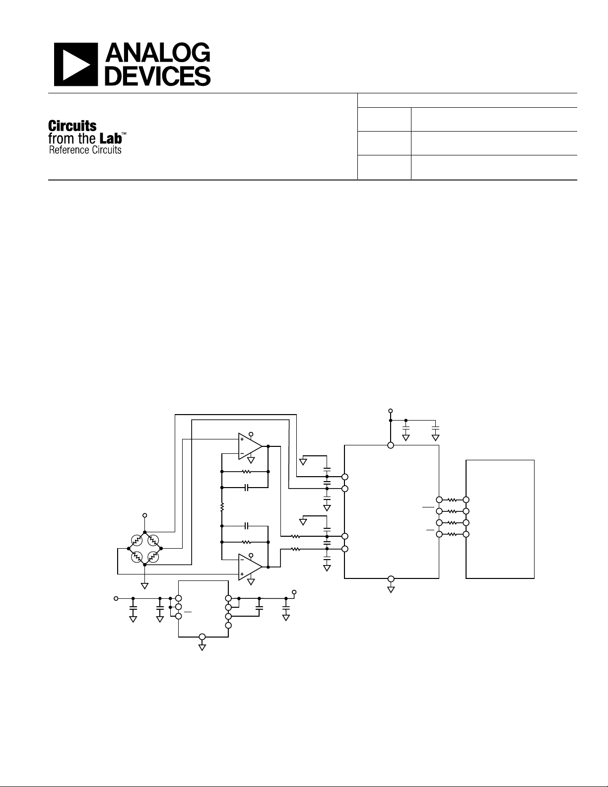
CIRCUIT FUNCTION AND BENEFITS
The circuit in Figure 1 is a precision weigh scale signal
conditioning system. It uses the AD7791, a low power buffered
24-bit sigma-delta ADC along with two external ADA4528-1
zero-drift amplifiers. This solution allows for high dc gain with
a single supply.
Ultralow noise, low offset voltage, and low drift amplifiers are
used at the front end for amplification of the low-level signal
from the load cell. The circuit yields 15.3 bit noise-free code
resolution for a load cell with a full-scale output of 10 mV.
This circuit allows great flexibility in designing a custom lowlevel signal conditioning front end that gives the user the ability
to easily optimize the overall transfer function of the combined
sensor-amplifier-converter circuit. The AD7791 maintains good
performance over the complete output data range, from 9.5 Hz
to 120 Hz, which allows it to be used in weigh scale applications
that operate at various low speeds.
Rev. 0
each circuit, and their function and performance have been tested and verified in a lab environment at
be liable f
Figure 1. Weigh Scale System Using the AD7791 (Simplified Schematic, All Connections and Decoupling Not Shown)
One Technology Way, P.O. Box 9106, Norwood, MA 02062-9106, U.S.A.
Tel: 781.329.4700
www.analog.com
Page 2
CN-0216 Circuit Note
CIRCUIT DESCRIPTION
Figure 2 shows the actual test setup. For testing purposes, a
6-wire Tedea-Huntleigh 505H-0002-F070 load cell is used.
Current flowing through a PCB trace produces an IR voltage
drop, and with longer traces, this voltage drop can be several
millivolts or more, introducing a considerable error. A 1 inch
long, 0.005 inch wide trace of 1 oz copper has a resistance of
approximately 100 mΩ at room temperature. With a load
current of 10 mA, this can introduce a 1 mV error.
A 6-wire load cell has two sense pins, in addition to the
excitation, ground, and two output connections. The sense pins
are connected to the high side (excitation pin) and low side
(ground pin) of the Wheatstone bridge. The voltage developed
across the bridge can be accurately measured regardless of the
voltage drop due to wire resistance. In addition, the AD7791
accepts differential analog inputs and a differential reference as
well. These two sense pins are connected to the AD7791
reference inputs to create a ratiometric configuration that is
immune to low frequency changes in the power supply
excitation voltage. The ratiometric connection eliminates the
need for a precision voltage reference.
Unlike a 6-wire load cell, a 4-wire load cell does not have sense
pins, and the ADC differential reference pins are connected
directly to the excitation voltage and ground. With this
connection, there exists a voltage difference between the
excitation pin and the reference pin on the ADC due to wire
resistance. There will also be a voltage difference on the low side
(ground) due to wire resistance. The system will not be
completely ratiometric.
The Tedea-Huntleigh 2 kg load cell has a sensitivity of 2 mV/V
and a full-scale output of 10 mV when the excitation voltage is
5 V. A load cell also has an offset, or TARE, associated with it.
In addition, the load cell also has a gain error. Some customers
use a DAC to remove or null the TARE. When the AD7791 uses
a 5 V reference, its differential analog input range is equal to
±5 V, or 10 V p-p. The circuit in Figure 1 amplifies the load cell
output by a factor of 375 (1 + 2R1/RG), so the full-scale input
range referred to the load cell output is 10 V/375 = 27 mV p-p.
This extra range relative to the 10 mV p-p load cell full-scale
signal is beneficial as it ensures that the offset and gain error of
the load cell do not overload the ADC’s front end.
The low-level amplitude signal from the load cell is amplified by
two ADA4528-1 zero-drift amplifiers. A zero-drift amplifier, as
the name suggests, has a close to zero offset voltage drift. The
amplifier continuously self-corrects for any dc errors, making it
as accurate as possible. Besides having low offset voltage and
drift, a zero-drift amplfier also exhibits no 1/f noise. This
important feature allows precision weigh scale measurement at
dc or low frequency.
The two ADA4528-1 op amps are configured as the first stage of
a three op amp instrumentation amplifier. A third op amp
connected as a difference amplifier would normally be used for
the second stage, but in the circuit of Figure 1, the differential
input of the AD7791 performs this function.
The gain is equal to 1 + 2R1/RG. Capacitors C1 and C2 are
placed in the feedback loops of the op amps and form 4.3 Hz
cutoff frequency low-pass filters with R1 and R2. This limits the
amount of noise entering the sigma-delta ADC. C5 in
conjunction with R3 and R4 form a differential filter with a
cutoff frequency of 8 Hz, which further limits the noise. C3 and
C4 in conjunction with R3 and R4 form common-mode filters
with a cutoff frequency of 159 Hz.
The ADP3301 low noise regulator powers the AD7791,
ADA4528-1, and the load cell. In addition to decoupling
capacitors, a noise reduction capacitor is placed on the regulator
output as recommended in the ADP3301 data sheet. It is
essential that the regulator is low noise, because any noise on
the power supply or ground plane introduces noise into the
system and degrades the circuit performance.
Figure 2. Weigh Scale System Setup Using the AD7791
The 24-bit sigma-delta ADC AD7791 converts the amplified
signal from the load cell. The AD7791 is configured to operate
in the buffered mode to accommodate the impedance of the
R-C filter network on the analog input pins.
Figure 3 shows the AD7791’s rms noise for different output data
rates. This plot shows that the rms noise increases as the output
data rate increases. However, the device maintains good noise
performance over the complete range of output data rates.
10164-002
Rev. 0 | Page 2 of 5
Page 3

Circuit Note CN-0216
100
10
1
0.1
1 10 100
OUTPUT DATA RATE (Hz)
RMS NOISE (µV)
1000
10164-003
705,688
Vμ1.16.6
V5
=
×
( )
( )
( )
bits5.19
2log
705,688log
705,688log
10
10
2
==
μV596.0
2
V10
LSB1
24
==
557,39
Vμ8.94
V3.75
=
( )
( )
( )
bits3.15
2log
557,39log
557,39log
10
10
2
==
10164-004
g05.0
557,39
kg2
=
Therefore, the corresponding noise-free code resolution of the
total system is:
Figure 4 shows a plot of the ADC codes for 500 samples
(52.6 sec for 9.5 Hz data rate). Note that the peak-to-peak
spread is about 160 codes.
Figure 3. AD7791 RMS Noise for Different Output Data Rates and a 2.5 V
The AD7791 rms noise of 1.1 µV for a 9.5 Hz output data rate
and a reference of 2.5 V yields the following number of noisefree counts:
Reference (5 V p-p Input Range), Buffer On
where the factor of 6.6 converts the rms voltage into a peak-topeak voltage.
The corresponding noise-free code resolution is, therefore:
Note that this represents the performance of the AD7791
without the load cell or the input amplifier connected.
The ADA4528-1 has 5.9 nV/√Hz of voltage noise density and,
therefore, the input amplifiers and resistors will add noise to the
system. In addition, the load cell itself will add noise.
In the circuit of Figure 1, a 5 V reference is used, therefore, the
peak-to-peak input range is 10 V. The LSB is, therefore, equal to
Figure 4. Measured Output Code for 500 Samples Showing
the Effects of Noise
Figure 5 shows the same data presented in a histogram. Figure 4
and Figure 5 show the actual (raw) conversions read back from
the AD7791. In practice, a digital post filter is typically used in a
weigh scale system. The additional averaging that is performed
in the post filter will further improve the number of noise-free
counts at the expense of a reduced data rate.
The resolution of the system in grams can be calculated by
The 10 mV p-p full-scale signal from the load cell produces a
3.75 V p-p signal into the ADC, which is approximately 38% of
the ADC range.
Seven sets of 500 samples each were taken with the load cell
connected (no load). The peak-to-peak code spread for each
sample set was calculated, and the seven values averaged to
yield a code spread of 159 counts. This corresponds to 159 ×
0.596 µV = 94.8 µV p-p noise based on a full-scale input to the
ADC of 3.75 V p-p.
Therefore, the number of noise-free counts is
As with any high accuracy circuit, proper layout, grounding,
and decoupling techniques must be employed. See Tutor ial
MT-031, Grounding Data Converters and Solving the Mystery of
AGND and DGND and Tutorial MT-101, Decoupling Techniques
for more details. A complete design support package for this
circuit note can be found at www.analog.com/CN0216-
DesignSupport.
Rev. 0 | Page 3 of 5
Page 4

CN-0216 Circuit Note
10164-005
Getting Started
Load the evaluation software by placing the CN0216 Evaluation
Software disc in the CD drive of the PC. Using My Computer,
locate the drive that contains the evaluation software disc and
open the Readme file. Follow the instructions contained in the
Readme file for installing and using the evaluation software.
Functional Block Diagram
See Figure 1 of this circuit note for the circuit block diagram,
and the PDF file “ EVA L-CN0216-SDPZ-SCH” for the circuit
schematics. This file is contained in the CN0216 Design
Support Package.
Setup
Connect the 120-pin connector on the EVA L-CN0216-SDPZ
circuit board to the connector marked “CON A” on the
EVA L-SDP-CB1Z evaluation (SDP) board. Nylon hardware
should be used to firmly secure the two boards, using the holes
provided at the ends of the 120-pin connectors. Connect the
Figure 5. Measured Histogram for 500 Samples Showing
the Effects of Noise
COMMON VARIATIONS
Other ADCs and circuits suitable for weigh scale applications
are discussed in CN-0102 (AD7190), CN-0107 (AD7780), CN-
0108 (AD7781), CN-0118 (AD7191), CN-0119 (AD7192), and
CN-0155 (AD7195).
The AD7171 is a 16-bit sigma-delta ADC.
For a lower power consumption solution, use the ADA4051-2.
The ADA4051-2 is a dual micropower, zero-drift amplifier with
only 20 µA of supply current per amplifier.
CIRCUIT EVALUATION AND TEST
This circuit uses the EVAL -CN0216-SDPZ circuit board and
the EVA L-SDP-CB1Z system demonstration platform (SDP)
evaluation board. The two boards have 120-pin mating
connectors, allowing for the quick setup and evaluation of the
circuit’s performance. The EVA L-CN0216-SDPZ board contains
the circuit to be evaluated, as described in this note, and the
SDP evaluation board is used with the CN-0216 evaluation
software to capture the data from the EVA L-CN0216-SDPZ
circuit board.
Equipment Needed
• PC with a USB port and Windows XP or Windows Vista
(32-bit), or Windows 7 (32-bit)
• EVA L-CN0216-SDPZ circuit evaluation board
• EVA L-SDP-CB1Z SDP evaluation board
• CN0216 evaluation software
• Tedea-Huntleigh 505H-0002-F070 load cell or equivalent
• Power supply: +6 V, o r +6 V “wall wart”
load cell the EVA L-CN0216-SDPZ board.
With power to the supply off, connect a +6 V power supply to
the pins marked “+6 V” and “GND” on the board. If available, a
+6 V "wall wart" can be connected to the barrel jack connector
on the board and used in place of the +6 V power supply.
Connect the USB cable supplied with the SDP board to the USB
port on the PC. Note: Do not connect the USB cable to the mini
USB connector on the SDP board at this time.
Test
Apply power to the +6 V supply (or “wall wart”) connected to
EVA L-CN0216-SDPZ circuit board. Launch the evaluation
software and connect the USB cable from the PC to the USB
mini-connector on the SDP board. The software will be able to
communicate to the SDP board if the Analog Devices System
Development Platform driver is listed in the Device Manager.
Once USB communications are established, the SDP board can
now be used to send, receive, and capture serial data from the
EVA L-CN0216-SDPZ board.
Information and details regarding how to use the evaluation
software for data capture can be found in the CN0216
Evaluation Software Readme file.
Information regarding the SDP board can be found in the
SDP User Guide.
Analyzing the Data
At least 500 samples of the ADC output data should be taken.
Once the sample set is exported to a spreadsheet program, such
as Excel, the samples can be analyzed. The standard deviation of
the samples is approximately equal to the rms noise, assuming a
Gaussian noise distribution. The peak-to-peak noise is
approximately equal to the rms value multiplied by 6.6.
The peak-to-peak noise can also be taken directly from the
sample set by simply taking the difference between the largest
and smallest sample. In practice, the results obtained using this
Rev. 0 | Page 4 of 5
Page 5

Circuit Note CN-0216
(Continued from first page) Circuits from the L ab circuits are intended only for use with Analog Devices products and are the intellectual property of Analog Devices or its licensors. While you
reserves the right to change any Circuits from the Lab circuits at any time without notice but is under no obligation to do so.
method were approximately the same as the value obtained by
multiplying the rms value by 6.6.
The values obtained from the sample set are in LSBs, so they
must be converted into voltage, where 1 LSB = 0.596 µV for a
5 V reference.
If desired, the results of several sample sets can be averaged to
get a more accurate measurement.
Noise-free code resolution is calculated from the peak-to-peak
noise as described previously in this circuit note.
LEARN MORE
Kester, Walt. 1999. Sensor Signal Conditioning. Section 2.
Analog Devices.
Kester, Walt. 1999. Sensor Signal Conditioning. Section 3.
Analog Devices.
Kester, Walt. 1999. Sensor Signal Conditioning. Section 4.
Analog Devices.
MT-004 Tutorial, The Good, the Bad, and the Ugly Aspects of
ADC Input Noise—Is No Noise Good Noise? Analog Devices.
MT-022 Tutorial, ADC Architectures III: Sigma-Delta ADC
Basics, Analog Devices.
MT-023 Tutorial, ADC Architectures IV: Sigma-Delta ADC
Advanced Concepts and Applications, Analog Devices.
MT-031 Tutorial, Grounding Data Converters and Solving the
Mystery of "AGND" and "DGND", Analog Devices.
MT-063 Tutorial, Basic Three Op Amp In-Amp Configuration,
Analog Devices.
MT-101 Tutorial, Decoupling Techniques, Analog Devices.
Wong, Vicky, AN-1114 Application Note, Lowest Noise Zero-
Drift Amplifier Has 5.6 nV/√Hz Voltage Noise Density,
Analog Devices.
CN-0102 Circuit Note, Precision Weigh Scale Design Using the
AD7190 24-Bit Sigma-Delta ADC with Internal PGA,
Analog Devices.
CN-0107 Circuit Note, Weigh Scale Design Using the AD7780
24-Bit Sigma-Delta ADC with Internal PGA, Analog
Devices.
CN-0108 Circuit Note, Weigh Scale Design Using the AD7781
20-Bit Sigma-Delta ADC with Internal PGA, Analog
Devices.
CN-0118 Circuit Note, Precision Weigh Scale Design Using the
AD7191 24-Bit Sigma-Delta ADC with Internal PGA,
Analog Devices.
CN-0119 Circuit Note, Precision Weigh Scale Design Using the
AD7192 24-Bit Sigma-Delta ADC with Internal PGA,
Analog Devices.
CN-0155 Circuit Note, Precision Weigh Scale Design Using a 24-
Bit Sigma-Delta ADC with Internal PGA and AC Excitation,
Analog Devices.
Data Sheets and Evaluation Boards
AD7791 Data Sheet
ADA4528-1 Data Sheet
ADP3301 Data Sheet
CN-0216 Circuit Evaluation Board (EVAL-CN0216-SDPZ)
System Demonstration Platform (EVAL-SDP-CB1Z)
REVISION HISTORY
9/11—Revision 0: Initial Version
may use the Cir cuits from the Lab circuits in the design of your product, no other license is granted by implication or otherwise under any patents or other intellectual property by
application or use of the Circuits from the Lab circuits. Informa tion furnished by Analog Devices is believed to be accurate and reliable. However, "Circuits from the Lab" are supplied "as is"
and without warranties of any kind, express, implied, or statutory including, but not limited to, any implied warranty of merchanta bility, noninfringement or fitness for a particular
purpose and no responsibility is assumed by Analog Devices for their use, nor for any infringements of patents or other rights of third parties that may result from their use. Analog Devices
©2011 Analog Devices, Inc. All rights reserved. Trademarks and
registered trademarks are the property of their respective owners.
CN10164-0-9/11(0)
Rev. 0 | Page 5 of 5
 Loading...