

Page 1
Circuit Note
Circuits from the Lab™ circuits from Analog Devices have been designed and built by Analog Devices
engineers. Standard engineering practices have been employed in the design and construction of
d their function and performance have been tested and verified in a lab environment at
room temperature. However, you are solely responsible for testing the circuit and determining its
be liable for direct, indirect, special, incidental, consequential or punitive damages due to any cause
6VLITHIUM ION
BATTERY
(2 × 3V CELLS)
LCD
DRIVER
LCD
AIN1(+)
DV
DD
AV
DD
AIN1(–)
AD7793
SCLK
DIN
DOUT/RDY
CS
IOUT1
AIN2(+)
AIN2(–)
REFIN(+)
REFIN(–)
0.1µF
0.01µF
+
–
0.01µF
1kΩ
1kΩ
THERMISTOR
KTY81-110
1kΩ AT 25°C
THERMOCOUPLE
COLD JUNCTION
THERMOCOUPLE
CONNECTOR
2kΩ
0.1%
10ppm
0.1µF
1.5Ω
10µF
+
+
ADuC832
ANALOG
MICRO-
CONTROLLER
CLK GND
IOUT2
09776-001
Circuits from the Lab™ reference circuits are engineered and
tested for quick and easy system integration to help solve today’s
analog, mixed-signal, and RF design challenges. For more
information and/or support, visit www.analog.com/CN0206.
Complete Thermocouple Measurement System Using the
AD7793 24-Bit Sigma-Delta ADC
EVALUATION AND DESIGN SUPPORT
Design and Integration Files
Schematics, Layout Files, Bill of Materials
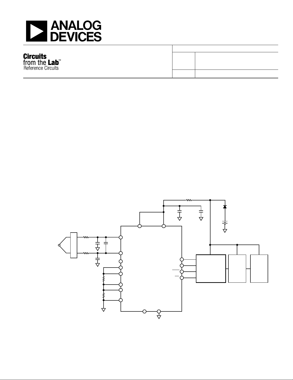
CIRCUIT FUNCTION AND BENEFITS
The circuit, shown in Figure 1, is a complete thermocouple system
based on the AD7793 24-bit sigma-delta ADC. The AD7793 is
a low power, low noise, complete analog front end for high
precision measurement applications. The device includes a
PGA, internal reference, internal clock, and excitation currents,
thereby greatly simplifying the thermocouple system design.
The system noise is approximately 0.02°C peak-to-peak.
CN-0206
Devices Connected/Referenced
3-Channel, Low Noise, Low Power,
AD7793
ADuC832 Precision Analog Microcontroller
The AD7793 consumes only 500 µA maximum, making
it suitable for any low power application, such as smart
transmitters where the complete transmitter must consume less
than 4 mA. The AD7793 also has a power down option. In this
mode, the complete ADC along with its auxiliary functions are
powered down so that the part consumes 1 µA maximum.
Since the AD7793 provides an integrated solution for
thermocouple design, it interfaces directly to the thermocouple.
For the cold junction compensation, a thermistor along with a
precision resistor is used. These are the only external
components required for the cold junction measurement
other than some simple R-C filters for EMC considerations.
24-Bit Σ-Δ ADC with On-Chip In-Amp
and Reference
Figure 1. Thermocouple Measurement System with Cold Junction Compensation (Simplified Schematic: All Connections and Decoupling Not Shown)
Rev.0
each circuit, an
suitability and applicability for your use and application. Accordingly, in no event shall Analog Devices
whatsoever connected to the use of any Circuits from the Lab circuits. (Continued on last page)
One Technology Way, P.O. Box 9106, Norwood, MA 02062-9106, U.S.A.
Tel: 781.329.4700
Fax: 781.461.3113 ©2011 Analog Devices, Inc. All rights reserved.
www.analog.com
Page 2
CN-0206 Circuit Note
20
15
10
5
0
–5
–10
–300 –200 –100 0 100 200 300 400
09776-002
THERMOCOUPLE EMF (mV)
TEMPERATURE (°C)
APPROXIMATELY
LINEAR REGION
TYPE “T” THERMOCOUPLE
CIRCUIT DESCRIPTION
A type "T" thermocouple is used in the circuit. This
thermocouple (made from copper and constantan) measures
temperature from −200°C to +400°C. It generates a typical
temperature dependent voltage of 40 µV/°C.
A thermocouple does not have a linear transfer function. For a
temperature range of 0°C to +60°C , the response is quite linear.
However, for wider temperature ranges, a linearization routine
is required.
The circuit tested does not include linearization. Therefore, the
useful measurement range of the circuit is from 0°C to +60°C.
For this temperature range, the thermocouple generates a
voltage from 0 mV to 2.4 mV. The internal 1.17 V reference is
used for the thermocouple conversions. So, the AD7793 is
configured for a gain of 128.
Since the AD7793 operates from a single power supply, the
signal generated by the thermocouple must be biased above
ground so that it is within the acceptable range of the ADC. For
a gain of 128, the absolute voltage on the analog inputs must be
between GND + 300 mV and AVDD – 1.1 V.
The bias voltage generator onboard the AD7793 biases the
thermocouple signal so that it has a common-mode voltage of
AVDD/2. This ensures that the input voltage limits are met with
significant margin.
The thermistor has a value of 1 kΩ at +25°C. The typical
resistance at 0°C is 815 Ω and 1040 Ω at +30°C. Assuming a
linear transfer function between 0°C and 30°C , the relationship
between cold junction temperature and thermistor resistance R is
Cold Junction Temperature = 30 × (R – 815)/(1040 – 815)
The 1 mA excitation current on the AD7793 is used to supply
the thermistor and the 2 kΩ precision resistor. The reference
voltage is generated using this external precision 2 kΩ resistor.
This architecture gives a ratiometric configuration—the
excitation current is used to supply the thermistor and to
generate the reference voltage. Therefore, any deviation in the
value of the excitation current does not alter the accuracy of the
system.
The AD7793 operates at a gain of 1 when sampling the
thermistor channel. For a maximum cold junction of +30°C,
the maximum voltage generated across the thermistor is 1 mA ×
1040 Ω = 1.04 V.
The precision resistor is chosen so that the maximum voltage
generated across the thermistor multiplied by the PGA gain is
less than or equal to the voltage generated across the precision
resistor.
For a conversion value of ADC_CODE, the corresponding
thermistor resistance R equals
One other consideration is the output compliance of the IOUT1
pin of the AD7793. When the 1 mA excitation current is used,
the output compliance equals AVDD – 1.1 V. From the previous
calculations, this specification is met since the maximum
voltage at IOUT1 equals the voltage across the precision resistor
plus the voltage across the thermistor, which equals 2 V + 1.04 V
= 3.04 V.
The AD7793 is configured to operate with an output data rate of
16.7 Hz. For every ten conversions read from the thermocouple,
one conversion is read from the thermistor. The resultant
temperature equals
The conversions from the AD7793 are processed by the
ADuC832 analog microcontroller, and the resultant
temperature is displayed on the LCD display.
The thermocouple design is operated from 6 V (2 × 3 V
Lithium Ion) batteries. A diode reduces the 6 V to a level
suitable for the AD7793 and the ADuC832 analog
microcontroller. An RC filter is placed between the ADuC832
power supply and the AD7793 power supply so that the power
supply digital noise to the AD7793 is minimized.
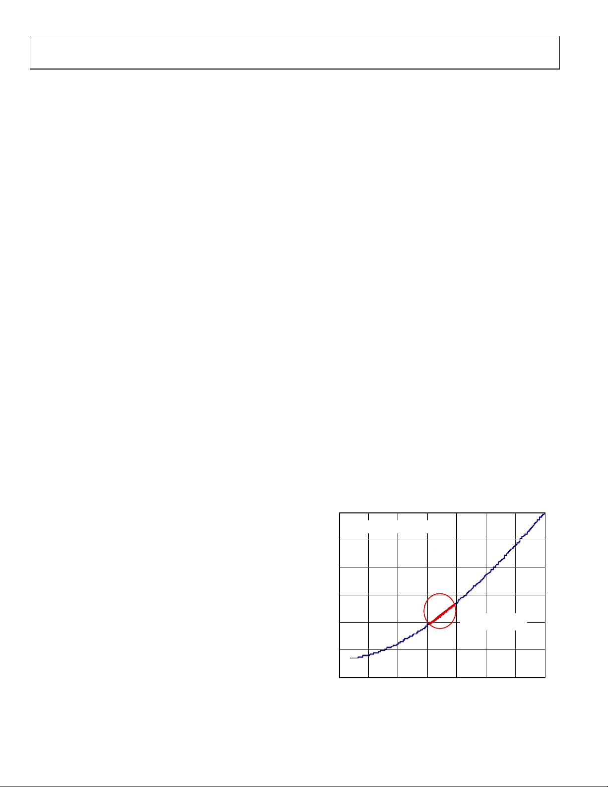
Figure 2 shows the relationship between voltage generated across
the thermocouple and temperature for a T-type thermocouple. The
circled area is the region from 0°C to +60°C where the transfer
function is approximately linear.
Rev. 0 | Page 2 of 4
R = (ADC_CODE – 0x800000) × 2000/2
23
Temperature = Thermocouple Temperature + Cold
Junction Temperature
Figure 2. Thermocouple EMF vs Temperature
Page 3

Circuit Note CN-0206
09776-003
When the system is at room temperature, the thermistor
should indicate the value of the ambient temperature. The
thermocouple indicates the relative temperature with respect to
the cold junction temperature, i.e., the temperature difference
between the cold junction (thermistor) and the thermocouple.
Therefore, at room temperature, the thermocouple should
indicate 0°C .
If the thermocouple is placed in an ice bucket, the thermistor
continues to measure the ambient (cold junction) temperature.
The thermocouple should indicate the negative of the
thermistor value so that the overall temperature equals zero.
Finally, for an output data rate of 16.7 Hz and a gain of 128, the
rms noise of the AD7793 equals 0.088 µV. The peak-to-peak
noise is
6.6 × RMS Noise = 6.6 × 0.088 µV = 0.581 µV
If the thermocouple has a sensitivity of precisely 40 µV/°C, the
thermocouple should measure the temperature to a resolution of
0.581 µV ÷ 40 µV = 0.014°C
Figure 3 shows the actual test board. The system was evaluated
by measuring the thermistor temperature, the thermocouple
temperature, and the resolution at room temperature and when
the thermocouple was placed in an ice bucket. The results are
shown in Table 1.
Table 1. Test Results for Thermocouple System
Ambient
0°C
Thermocouple Reading (°C) −20 0
Thermistor Reading (°C)
Resultant Reading (°C)
Peak-to-Peak Noise (°C )
20.3 20.3
0.3 20.3
0.02 0.02
Temperature (20°C)
From Table 1, the thermocouple is reporting the correct value,
while the thermistor has a 0.3°C error. This is the accuracy of
the system when linearization is not included. Including
linearization for the thermocouple and the thermistor would
improve the accuracy of the system, and it would also allow the
system to measure a wider range of temperatures.
If the difference between the minimum and maximum
temperature readings is measured for every 10 readings, the
peak-to-peak noise in terms of temperature is 0.02°C.
Therefore, the actual peak-to-peak resolution is very close to
the expected value.
COMMON VARIATIONS
The AD7793 is a low noise, low power ADC. Other suitable
ADCs are the AD7792 and AD7785. Both parts have the same
feature set as the AD7793. However, the AD7792 is a 16-bit
ADC while the AD7785 is a 20-bit ADC.
CIRCUIT EVALUATION AND TEST
Test data was taken using the board shown in Figure 3.
Complete documentation for the system can be
found in the CN-0206 Design Support package at
www.analog.com/CN0206-DesignSupport.
LEARN MORE
CN-0206 Design Support Package:
www.analog.com/CN0206-DesignSupport
Kester, Walt. 1999. Sensor Signal Conditioning. Section 7.
Analog Devices.
MT-004 Tutorial, The Good, the Bad, and the Ugly Aspects of
ADC Input Noise—Is No Noise Good Noise? Analog Devices.
Figure 3. Thermocouple System Using the AD7793
Rev. 0 | Page 3 of 4
MT-022 Tutorial, ADC Architectures III: Sigma-Delta ADC
Basics, Analog Devices.
MT-023 Tutorial, ADC Architectures IV: Sigma-Delta ADC
Advanced Concepts and Applications, Analog Devices.
MT-031 Tutorial, Grounding Data Converters and Solving the
Mystery of "AGND" and "DGND", Analog Devices.
Page 4

CN-0206 Circuit Note
MT-101 Tutorial, Decoupling Techniques, Analog Devices.
Data Sheets and Evaluation Boards
AD7793 Data Sheet
AD7793 Evaluation Board
ADuC832 Data Sheet
ADuC832 Evaluation System
REVISION HISTORY
10/11—Revision 0: Initial Version
(Continued from first page) Circuits from the Lab circuits are intended only for use with Analog Devices products and are the intellectual property of Analog Devices or its licensors. While
you may use the Circuits from the Lab circuits in the design of your product, no other license is granted by implication or otherwise under any patents or other intellectual property by
application or use of the Circuits from the Lab circuits. Information furnished by Analog Devices is believed to be accurate and reliable. However, "Circuits from the Lab" are supplied "as is"
and without warranties of any kind, express, implied, or statutory including, but not limited to, any implied warranty of merchantability, noninfringement or fitness for a particular
purpose and no responsibility is assumed by Analog Devices for their use, nor for any infringements of patents or other rights of third pa rties that may result from their use. Analog Devices
reserves the right to change any Circuits from the Lab circuits at any time without notice but is under no obligation to do so.
©2011 Analog Devices, Inc. All rights reserved. Trademarks and
registered trademarks are the property of their respective owners.
CN09776-0-10/11(0)
Rev. 0 | Page 4 of 4
 Loading...