

Page 1
Circuit Note
Circuits from the Lab™ circuits from Analog Devices have been designed and built by Analog Devices
each circuit, and their function and performance have been tested and verified in a lab environment at
room temperature. However, you are solely responsible for testing the circuit and determining its
suitability and applicability for your use and application. Accordingly, in no event shall Analog Devices
be liable for direct, indirect, special, incidental, consequential or punitive damages due to any cause
+
+
+
+
+
968 3 2
15 17 16 19
20
24
1
CLR
IOV
CCVCCVDD
BUFFERED
V
REFP
V
REFP
V
SS
V
REFN
AGND
–10V TO +10V
OUTPUT
VOLTAGE
0V TO +10V
DGND
V
OUT
R
FB
7
LDAC
11
SDO
14
INV
13
SCLK
SYNC
AD5780
AD8675
AD8675
12
SDIN
4
RESET
+15V
+15V
+10V
–15V
–15V
10µF
C1
10µF
A1
A2
0.1µF
10µF
+3.3V +15V
+15V
–15V
0.1µF
10µF
0.1µF
10µF
0.1µF
0.1µF
R1
1.5kΩ
R3*
1kΩ
6.8kΩ
6.8kΩ
SPI INTERFACE
AND DIGITAL
COTNROL
R2*
1kΩ
ADR445
GND
V
INVOUT
09697-001
*FOR OPTIMUM PERFORMANCE OVER TEMPERATURE,
R2 AND R3 SHOULD BE IN A SINGLE PACKAGE.
Circuits from the Lab™ reference circuits are engineered and
tested for quick and easy system integration to help solve today’s
analog, mixed-signal, and RF design challenges. For more
information and/or support, visit www.analog.com/CN0200.
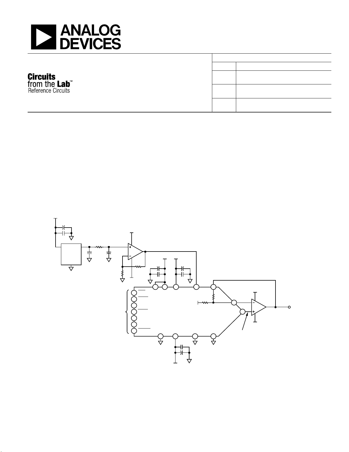
18-Bit, Linear, Low Noise, Precision Bipolar ±10 V DC Voltage Source
EVALUATION AND DESIGN SUPPORT
Circuit Evaluation Boards
AD5780 Circuit Evaluation Board (EVAL-AD5780SDZ)
System Demonstration Platform (EVAL-SDP-CB1Z)
Design and Integration Files
Schematics, Layout Files, Bill of Materials
CIRCUIT FUNCTION AND BENEFITS
The circuit shown in Figure 1 is an 18-bit linear, low noise,
precision bipolar (±10 V) voltage source with a minimum
CN-0200
Devices Connected/Referenced
AD5780 True 18-Bit, Voltage Output DAC
AD8675
AD8676
ADR445
amount of external components. The AD5780 DAC is an 18-bit,
unbuffered voltage output DAC operating from a bipolar supply
of up to 33 V. The AD5780 accepts a positive reference input
range of 5 V to VDD − 2.5 V, and a negative reference input
range of VSS + 2.5 V to 0 V. Both reference inputs are buffered
on the chip, and external buffers are not required. The AD5780
offers a relative accuracy specification of ±1 LSB maximum, and
operation is guaranteed monotonic, with a ±1 LSB maximum
DNL specification.
Ultraprecision, 36 V, 2.8 nV√Hz,
Rail-to-Rail Output Op Amp
Ultraprecision, 36 V, 2.8 nV√Hz, Dual
Rail-to-Rail Output Op Amp
Ultralow Noise 5V LDO XFET® Voltage
Reference
Rev.0
engineers. Standard engineering practices have been employed in the design and construction of
whatsoever connected to the use of any Circuits from the Lab circuits. (Continued on last page)
Figure 1. 18-Bit Accurate, +10 V Voltage Source (Simplified Schematic: All Connections and Decoupling Not Shown)
One Technology Way, P.O. Box 9106, Norwood, MA 02062-9106, U.S.A.
Tel: 781.329.4700
Fax: 781.461.3113 ©2011 Analog Devices, Inc. All rights reserved.
www.analog.com
Page 2
CN-0200 Circuit Note
–0.4
–0.3
–0.2
–0.1
0
0.1
0.2
0.3
0.4
0.5
0.6
0 50000 100000 150000 200000 250000
INL (LSB)
DAC CODE
09697-002
–0.2
–0.1
0
0.1
0.2
0.3
0.4
0.5
0 50000 100000 150000 200000 250000
DNL (LSB)
DAC CODE
09697-003
The AD8675 precision op amp has low offset voltage (75 µV
maximum), low noise (2.8 nV/√Hz typical), and is an optimum
output buffer for the AD5780. The AD5780 has two internal
matched feedforward and feedback resistors, which are
connected to the AD8675 op amp and provide the 10 V offset
voltage. This allows an output voltage swing of ±10 V with a
single external 10 V reference.
The digital input to the circuit is serial and is compatible with
standard SPI, QSPI, MICROWIRE®, and DSP interface standards.
For high accuracy applications, the compact circuit offers high
precision, as well as low noise—this is ensured by the
combination of the AD5780, ADR445, and AD8675 precision
components.
This combination of parts provides industry-leading 18-bit
integral nonlinearity (INL) of ±1 LSB and differential
nonlinearity (DNL) of ±0.75 LSB, with guaranteed
monotonicity, as well as low power, small PCB area, and
cost effectiveness in an LFCSP package.
CIRCUIT DESCRIPTION
The digital-to-analog converter (DAC) shown in Figure 1 is the
AD5780, a high voltage, 18-bit converter with SPI interface,
offering ±1 LSB INL, ±0.75 LSB DNL, and 7.5 nV/√Hz noise
spectral density. The AD5780 also exhibits an extremely low
temperature drift of 0.005 LSB/°C.
Figure 1 shows the AD5780 configured in a gain-of-two mode
such that a single reference source can be used to generate a
symmetrical bipolar output voltage range. This mode of
operation uses an external op amp (A2), as well as on-chip
resistors (see AD5780 data sheet), to provide the gain of 2.
These internal resistors are thermally matched to each other
and to the DAC ladder resistance, resulting in ratiometric
thermal tracking. The output buffer is again the AD8675, used
for its low noise and low drift. This amplifier is also used (A1)
to amplify the +5 V reference voltage from the low noise
ADR445 to +10 V. R2 and R3 in this gain circuit are precision
metal foil resistors with 0.01% tolerance and a temperature
coefficient resistance of 0.6 ppm/°C. For optimum performance
over temperature, R1 and R2 should be in a single package, such
as the Vishay 300144 or VSR144 series. R2 and R3 are selected
to be 1 kΩ to keep noise in the system low. R1 and C1 form a
low-pass filter with a cutoff frequency of approximately 10 Hz.
The purpose of this filter is to attenuate voltage reference noise.
Linearity Measurements
The precision performance of the circuit shown in Figure 1 is
demonstrated on the EVAL -AD5780SDZ evaluation board
using an Agilent 3458A Multimeter. Figure 2 shows the integral
nonlinearity as a function of DAC code is within specifications
of ±1 LSB.
Figure 2. Integral Nonlinearity vs. DAC Code
Figure 3 shows that the differential nonlinearity as a function of
DAC code is within the −0.25 LSB to +0.75 LSB specification.
Figure 3. Differential Nonlinearity vs. DAC Code
Noise Drift Measurements
To be able to realize high precision, the peak-to-peak noise at
the circuit output must be maintained below 1 LSB, which is
76.29 µV for 18-bit resolution and a 20 V peak-to-peak voltage
range.
A real-time noise application will not have a high-pass cutoff at
0.1 Hz to attenuate 1/f noise but will include frequencies down
to dc in its pass band. With this in mind, the measured peak-topeak noise is realistically shown in Figure 4. In this case, the
noise at the output of the circuit was measured over a period of
100 seconds, effectively including frequencies as low as 0.01 Hz
in the measurement. The upper frequency cutoff is at approximately 14 Hz and is limited by the measurement setup.
Rev. 0 | Page 2 of 6
Page 3

Circuit Note CN-0200
–40
–30
–20
–10
0
10
30
20
40
0 20 40 60 80 100
NOISE (µV)
TIME (Seconds)
09697-004
V
DD
= +15V
V
SS
= –15V
V
REFP
= +10V
V
REFN
= 0V
ZERO SCALE
HALF SCALE
FULL SCALE
–3
–2
–1
0
1
3
2
4
0 20 40 60 80 100
NOISE (µV)
TIME (Seconds)
09697-005
VDD = +15V
V
SS
= –15V
V
REFP
= +10V
V
REFN
= 0V
HALF SCALE
FULL SCALE
ZERO SCALE
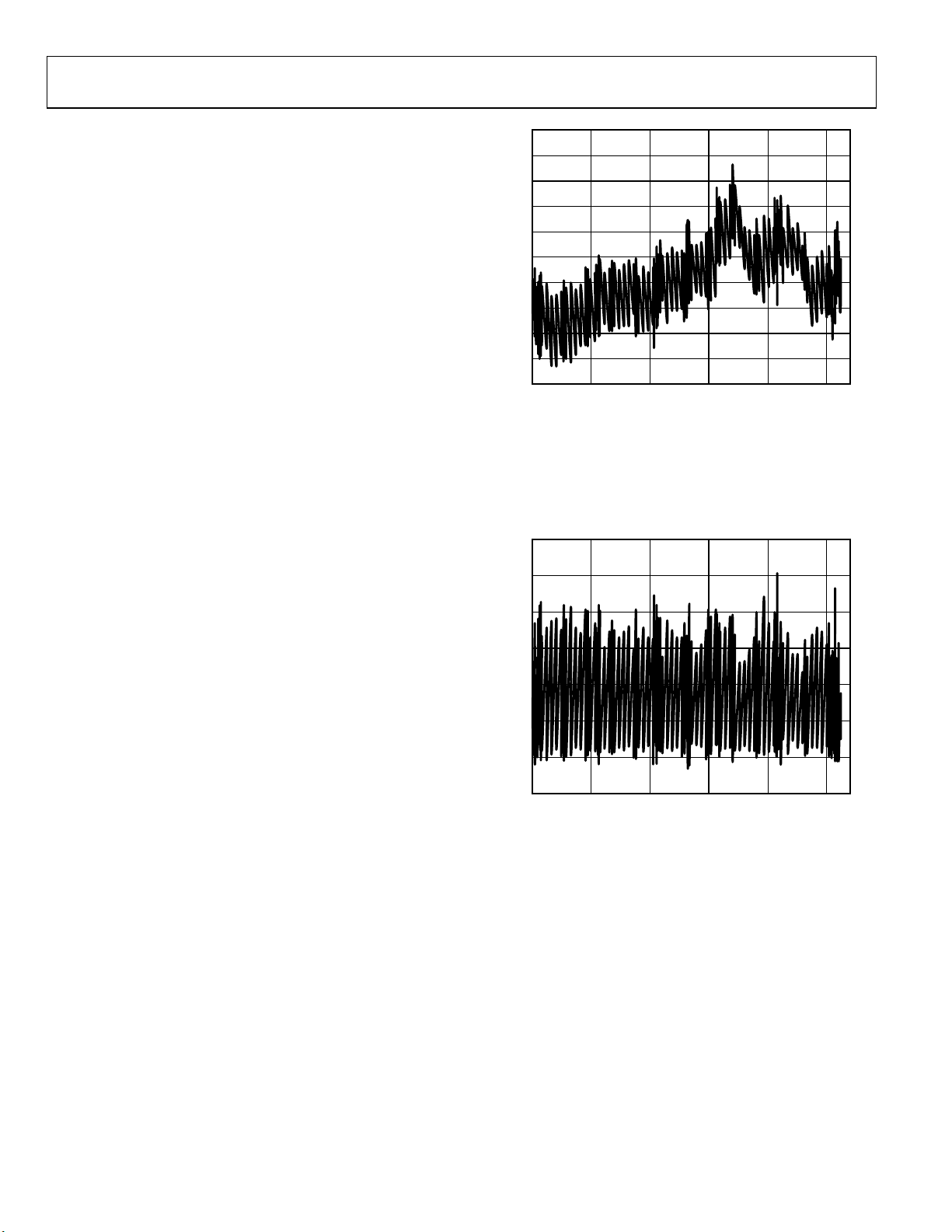
Figure 4 shows the peak-to-peak values are 1.2 µV for zero-scale
output, 32 µV for half-scale output, and 64 µV for full-scale
output.
The zero-scale output voltage exhibits the lowest noise because
it represents the noise from the DAC core only. The noise
contribution from each voltage reference path is attenuated by
the DAC when the zero-scale code is selected.
Figure 4. DAC Output Voltage Noise Measured Over 100 Second Period for
As the time period over which the measurement is taken is
increased, lower frequencies will be included, and the peak-topeak value will increase. At low frequencies, temperature drift
and thermocouple effects become contributors to noise. These
effects can be minimized by choosing components with low
thermal coefficients. In this circuit, the main contributor to low
frequency 1/f noise is the voltage reference. It also exhibits the
greatest temperature coefficient value in the circuit of 3 ppm/°C.
A temperature controlled ultralow noise reference would be
required to improve the half-scale and full-scale DAC output
noise.
Figure 5 shows the performance of the signal chain by replacing
the ADR445 with a Krohn Hite Model 523 Precision Reference
set for +5 V.
Complete schematics and layout of the printed circuit board
can be found in the CN-0200 Design Support Package:
www.analog.com/CN0200-DesignSupport .
Full Scale (Red), Half Scale (Green), and Zero Scale (Blue)
Figure 5. DAC Output Voltage Noise Measured Over 100 Second Period for
Full Scale (Red), Half Scale (Green), and Zero Scale (Blue) with Precision
Reference Source
COMMON VARIATIONS
The AD5780 will support a wide variety of output ranges from
0 V to +5 V up to ±10 V, and values in between. The gain-of-2
configuration, as shown in Figure 1, can be used if a
symmetrical output range is required. This mode is selected by
setting the RBUF bit of the AD5780 internal control register to
a Logic 0. If an asymmetrical range is required, individual
references can be applied at VREFP and VREFN, and the output
buffer should be configured for unity gain as described in the
AD5780 data sheet. This is done by setting the RBUF bit of the
AD5780 internal control register to a Logic 1.
The AD8676 is a dual version of the AD8675 op amp and can be
used in the circuit if desired.
CIRCUIT EVALUATION AND TEST
Equipment Required
• System Demonstration Platform (EVA L-SDP-CB1Z)
• E VAL -AD5780SDZ Evaluation Board and Software
• Agilent 3458A multimeter
• PC (Windows 32-bit or 64-bit)
• National Instruments GPIB to USB-B interface cable
• SMB cable (1)
Software Installation
The AD5780 evaluation kit includes self-installing software on
a CD. The software is compatible with Windows XP (SP2) and
Vista (32-bit and 64-bit). If the setup file does not run
automatically, you can run the setup.exe file from the CD.
Rev. 0 | Page 3 of 6
Page 4

CN-0200 Circuit Note
09697-006
Install the evaluation software before connecting the evaluation
board and SDP board to the USB port of the PC to ensure that
the evaluation system is correctly recognized when connected to
the PC.
1. After installation from the CD is complete, power up
the AD5780 evaluation board as described in the
Power Supplies section of UG-256. Connect the SDP
board (via either Connector A or Connector B) to the
AD5780 evaluation board and then to the USB port of
your PC using the supplied cable.
2. When the evaluation system is detected, proceed
through any dialog boxes that appear. This completes
the installation.
Functional Diagram
A functional diagram of the test setup is shown in Figure 7.
Power Supply Configuration
The following supplies must be provided:
• 3.3 V between the VCC and DGND on Connector J1
for the digital supply of the AD5780. Alternatively,
place Link 1 in Position A to power the digital
circuitry from the USB port via the SDP board
(default setting).
• +12 V to +16.5 V between the VDD and AGND inputs
of J2 for the positive analog supply of the AD5780.
• −12 V to −16.5 V between the VSS and AGND inputs
of J2 for the negative analog supply of the AD5780.
Figure 6. Evaluation Software Main Window
Rev. 0 | Page 4 of 6
Page 5

J2-3
+VDD
−15V
AGND
DUAL POWER SUPPLY
SDP
CON A
OR
CON B
120-PIN SDP
USB
PC
AGILENT
3458A MULTIMETER
GPIB
USB
USB
SMB
EVAL-AD5780SDZ
VOUT_BUF
−VSS
J2-2 J2-1
+15V
J4
COM
09697-007
Circuit Note CN-0200
Figure 7. Functional Block Diagram of Test Setup
Link Configuration Setup
The default link options are listed in Table 1. By default, the
board is configured with VREFP = +10 V and VREFN = −10 V
for a ±10 V output range.
Table 1. Default Link Options
Link No. Option
LK1 A
LK2 B
LK3 A
LK4 Removed
LK5 Removed
LK6 Removed
LK7 Removed
LK8 C
LK9 Inserted
LK11 Inserted
To configure the board for the circuit shown in Figure 1,
the following changes must be made to the default link
configuration in Table 1:
1. Place LK3 in position B.
2. Insert LK4.
3. Place LK8 in position B.
These changes configure the output buffer amplifier for a gain
of 2 and connect the VREFN pin of the AD5780 to ground.
Please refer to User Guide UG-256 for more information on the
EVA L-AD5780SDZ test setup.
Rev. 0 | Page 5 of 6
Test
The VOUT_BUF SMB connector is connected to the Agilent
3458A multimeter. The linearity measurements are run using
the Measure DAC Output Tab on the AD5780 GUI.
The noise drift measurement is measured on the VOUT_BUF
SMB connector also. The output voltage is set using the Prgram
Voltage tab in the AD5780 GUI. The peak-to-peak noise drift is
measured over 100 seconds.
For more details on the definitions and how to calculate the
INL, DNL, and noise from the measured data, see the
"TERMINOLOGY" section of the AD5780 data sheet and also
the following reference: Data Conversion Handbook, "Testing
Data Converters," Chapter 5, Analog Devices.
LEARN MORE
CN-0200 Design Support Package:
www.analog.com/CN0200-DesignSupport
Egan, Maurice. "The 20-Bit DAC Is the Easiest Part of a 1-ppm-
Accurate Precision Voltage Source," Analog Dialogue, Vol.
44, April 2010.
Kester, Walt. 2005. The Data Conversion Handbook. Analog
Devices. Chapters 3, 5, and 7.
MT-015 Tutorial, Basic DAC Architectures II: Binary DACs.
Analog Devices.
MT-016 Tutorial, Basic DAC Architectures III: Segmented DACs.
Analog Devices.
Page 6

CN-0200 Circuit Note
MT-031 Tutorial, Grounding Data Converters and Solving the
Mystery of AGND and DGND. Analog Devices.
MT-035 Tutorial, Op Amp Inputs, Outputs, Single-Supply, and
Rail-to-Rail Issues. Analog Devices.
MT-101 Tutorial, Decoupling Techniques. Analog Devices.
Voltage Reference Wizard Design Tool.
CN-0177 Circuit Note, 18-Bit, Linear, Low Noise, Precision
Bipolar ±10 V DC Voltage Source.
CN-0191 Circuit Note, 20-Bit, Linear, Low Noise, Precision,
Bipolar ±10 V DC Voltage Source.
User Guide UG-256 for EVA L-AD5780SDZ.
Data Sheets and Evaluation Boards
AD5780 Data Sheet and Evaluation Board
AD8676 Data Sheet
ADR445 Data Sheet
REVISION HISTORY
11/11—Revision 0: Initial Version
(Continued from first page) Circuits from the La b circuits are intended only for use with Analog Devices products and are the intellectual property of Analog Devices or its licensors. While you
may use the Circuits from the Lab circuits in the design of your product, no other license is granted by implication or otherwise under any patents or other intellectual property by
application or use of the Circuits from the Lab circuits. Information furnished by Analog Devices is believed to be accurate and reliable. However, "Circuits from the Lab" are supplied "as is"
and without warranties of any kind, express, implied, or statutory including, but not limited to, any implied warranty of merchantability, noninfringement or fitness for a particular
purpose an d no responsibil ity is assumed by Analog Devices for their use, nor for any infringements of patents or other rights of third parties that may result from their use. Analog Devices
reserves the right to change any Circuits from the Lab circuits at any time without notice but is under no obligation to do so.
©2011 Analog Devices, Inc. All rights reserved. Trademarks and
registered trademarks are the property of their respective owners.
CN09697-0-11/11(0)
Rev. 0 | Page 6 of 6
 Loading...