

Page 1
Circuit Note
150 mA, Low Quiescent Current, CMOS Linear
engineers. Standard engineering practices have been employed in the design and construction of
room temperature. However, you are solely responsible for testing the circuit and determining its
suitability and applicability for your use and application. Accordingly, in no event shall Analog Devices
U3-A
U3-D
U1
COMM
ENBL
VA1
VA2
VB1
VB2
D
CAP
B
D
CAP
A
0.47µF
27Ω
27Ω
27Ω
AGND DGND
10kΩ
10kΩ
0.47µF
220Ω
220Ω
220Ω
442Ω
75Ω
+3.3V
C
FLTR
*
+3.3V
0.01µF 0.01µF
RFIN
0.01µF
0.1µF1000pF
+3.3V+3.3V
AVDD
DVDD
VDRIVE
CS
DOUTA
SCLK
ADP121
ADL5502
AD7266
+5.5V
+3.3V
1µF
VIN
FLTR
VPOS
RFIN
VRMS
PEAK
CNTL
VOUT
EN
GND
1µF
SDP
BOARD
AND
SUPPORT
CIRCUITS
NOTE: U2 AND U3 ARE ADA4891- 4
CONTROL
(HIGH RESET;
LOW PE AK HOLD)
U5
U6
+1.25V
+1.25V
+2.5V
* *
* *
*SEE TEXT
8
4
1
2
3
7
6
5
U2-B
U3-B
27Ω
U2-D
10kΩ
10kΩ
0.47µF
220Ω
220Ω
220Ω
442Ω
+3.3V
U3-D
U3-A
0.47µF
+2.5V
U2-A
U2-C
U3-C
09569-001
Circuits from the Lab™ reference circuits are engineered and
tested for quick and easy system integration to help solve today’s
analog, mixed-signal, and RF design challenges. For more
information and/or support, visit www.analog.com/CN0187.
Crest Factor, Peak, and RMS RF Power Measurement Circuit Optimized for
High Speed, Low Power, and Single 3.3 V Supply
EVALUATION AND DESIGN SUPPORT
Circuit Evaluation Boards
CN-0187 Circuit Evaluation Board (EVAL-CN0187-SDPZ)
System Demonstration Platform (EVAL-SDP-CB1Z)
Design and Integration Files
Schematics, Layout Files, Bill of Materials
CN-0187
Devices Connected/Referenced
ADL5502 450 MHz to 6 GHz Crest Factor Detector
Differential/Single-Ended Input, Dual,
AD7266
ADA4891-4
ADP121
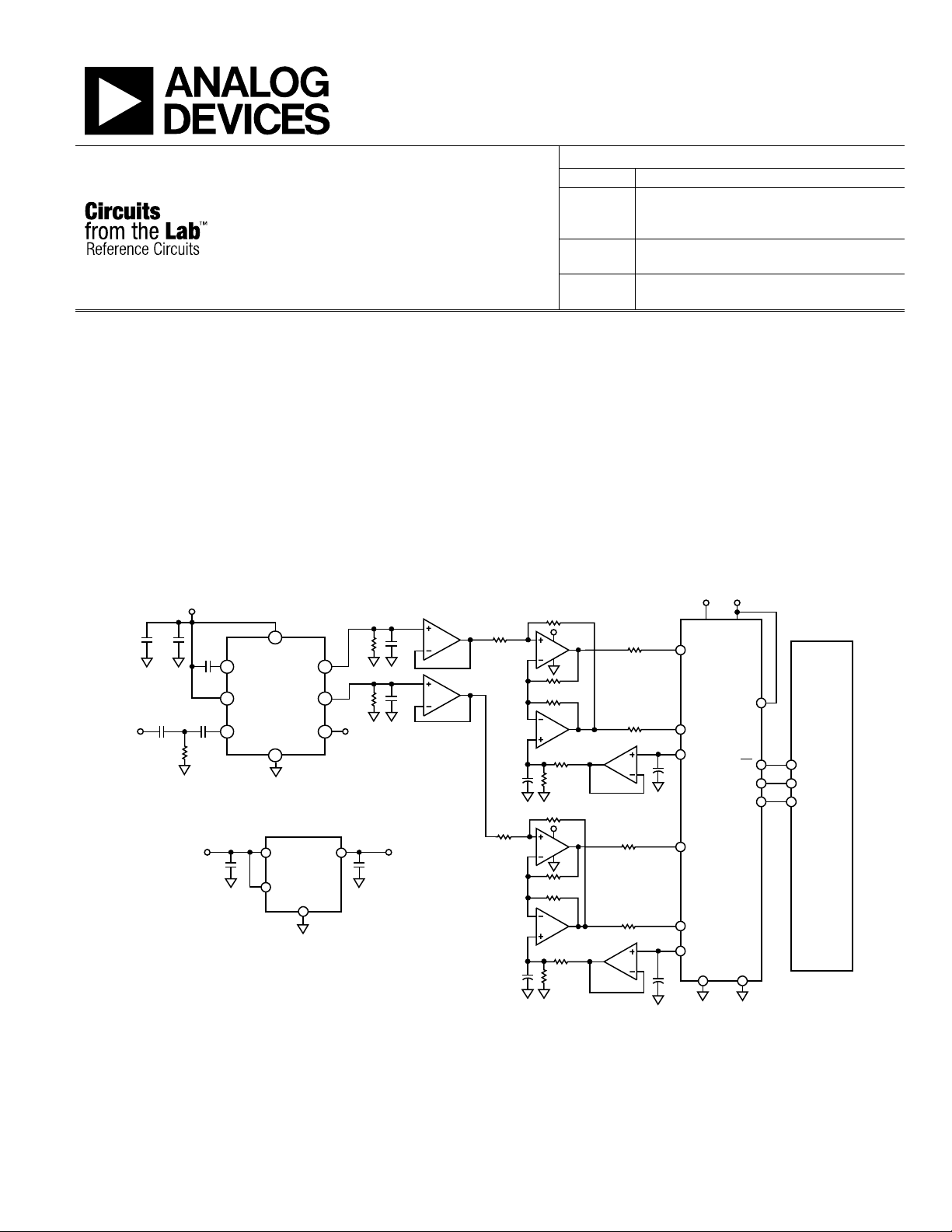
CIRCUIT FUNCTION AND BENEFITS
The circuit shown in Figure 1 measures peak and rms power
at any RF frequency from 450 MHz to 6 GHz over a range of
approximately 45 dB. The measurement results are converted
to differential signals in order to eliminate noise and are
provided as digital codes at the output of a 12-bit SAR ADC
with serial interface and integrated reference. A simple twopoint calibration is performed in the digital domain.
Simultaneous Sampling, 2 MSPS, 12-Bit,
3-Channel SAR Analog-to-Digital Converter
Low Cost, Quad, CMOS, High Speed, Rail-toRail Amplifier
Regulator in 5-Lead TSOT or 4-Ball WLCSP
Figure 1. High Speed, Low Power, Crest Factor, Peak, and RMS Power Measurement System (Simplified Schematic: All connections and Decoupling Not Shown)
Rev.0
Circuits from the Lab™ circuits from Analog Devices have been designed and built by Analog Devices
each circuit, and their function and performance have been tested and verified in a lab environment at
be liable for direct, indirect, special, incidental, consequential or punitive damages due to any cause
whatsoever connected to the use of any Circuits from the Lab circuits. (Continued on last page)
One Technology Way, P.O. Box 9106, Norwood, MA 02062-9106, U.S.A.
Tel: 781.329.4700
Fax: 781.461.3113 ©2011 Analog Devices, Inc. All rights reserved.
www.analog.com
Page 2

CN-0187 Circuit Note
The ADL5502 is a mean-responding (true rms) power detector
in combination with an envelope detector to accurately
determine the crest factor (CF) of a modulated signal. It can be
used in high frequency receiver and transmitter signal chains
from 450 MHz to 6 GHz with envelope bandwidths over 10 MHz.
The peak-hold function allows the capture of short peaks in the
envelope with lower sampling rate ADCs. Total current
consumption is only 3 mA @ 3 V.
The ADA4891-4 is a high speed, quad, CMOS amplifier that
offers high performance at a low cost. Current consumption is
only 4.4 mA/amplifier at 3 V. The amplifier features true singlesupply capability, with an input voltage range that extends 300 mV
below the negative rail. The rail-to-rail output stage enables
the output to swing to within 50 mV of each rail, ensuring
maximum dynamic range. Low distortion and fast settling time
makes it ideal for this application.
The AD7266
is a dual, 12-bit, high speed, low power, successive
approximation ADC that operates from a single 2.7 V to 5.25 V
power supply and features sampling rates up to 2 MSPS. The
device contains two ADCs, each preceded by a 3-channel
multiplexer, and a low noise, wide bandwidth track-and-hold
amplifier that can handle input frequencies in excess of 30 MHz.
Current consumption is only 3 mA at 3 V. It also contains an
internal 2.5 V reference.
The circuit operates on a single +3.3 V supply from the
ADP121, a low quiescent current, low dropout, linear regulator
that operates from 2.3 V to 5.5 V and provides up to 150 mA
of output current. The low 135 mV dropout voltage at 150 mA
load improves efficiency and allows operation over a wide input
voltage range. The low 30 μA of quiescent current at full load
makes the ADP121 ideal for battery-operated portable equipment.
The ADP121 is available in output voltages ranging from 1.2 V
to 3.3 V. The parts are optimized for stable operation with small
1 μF ceramic output capacitors. The ADP121 delivers good
transient performance with minimal board area.
Short-circuit protection and thermal overload protection
circuits prevent damage in adverse conditions. The ADP121 is
available in tiny 5-lead TSOT and 4-ball, 0.4 mm pitch halidefree WLCSP packages and utilizes the smallest footprint
solution to meet a variety of portable applications.
CIRCUIT DESCRIPTION
The RF signal being measured is applied to the ADL5502.
A single 75 Ω termination resistor at the RF input in parallel
with the input impedance of the ADL5502 provides a
broadband match of 50 Ω. More precise resistive or reactive
matches can be applied for narrow frequency band use (see
the RF Input Interfacing section of the ADL5502 data sheet).
The internal filter capacitor of the ADL5502 provides averaging
in the square domain but leaves some residual ac on the output.
Signals with high peak-to-average ratios, such as W-CDMA or
CDMA2000, can produce ac residual levels on the ADL5502
VRMS dc output. To reduce the effects of these low frequency
components in the waveforms, some additional filtering is
required. The internal square-domain filter capacitance of the
ADL5502 can be augmented by connecting a C
capacitor
FLTR
between Pin 1 (FLTR) and Pin 2 (VPOS). The ac residual can be
reduced further by adding capacitance to the VRMS output.
The combination of the internal 100 Ω output resistance and
the added output capacitance
produces a low-pass filter to
reduce output ripple of the VRMS output (see the Selecting the
Square-Domain Filter and Output Low-Pass Filter section of the
ADL5502 data sheet for more details).
To measure the peak of a waveform, the control line (CNTL)
must be temporally set to a logic high (reset mode for >1 µs)
and then set back to a logic low (peak-hold mode). This allows
the ADL5502 to be initialized to a known state. When setting
the device to measure peak, peak-hold mode should be toggled
for a period in which the input rms power and crest factor (CF)
is not likely to change.
If the ADL5502 is in peak-hold mode and the CF changes from
high to low or the input power changes from high to low, a
faulty peak measurement is reported. The ADL5502 simply
keeps reporting the highest peak that occurred when the peakhold mode was activated and the input power or the CF was
high. Unless CNTL is reset, the PEAK output does not reflect
the new peak in the signal.
The ADL5502 is capable of sourcing a VRMS output current of
approximately 3 mA. The output current is sourced through the
on-chip, 100 Ω series resistor; therefore, any load resistor forms
a voltage divider with this on-chip resistance. It is
recommended that the ADL5502 VRMS output drive high
resistive loads to preserve output swing. If an application
requires driving a low resistance load (as well as in cases where
increasing the nominal conversion gain is desired), a buffering
circuit is necessary.
The PEAK output is designed to drive 2 pF loads. It is
recommended that the ADL5502 PEAK output drive low
capacitive loads to achieve a full output response time. The
effects of larger capacitive loads are particularly visible when
tracking envelopes during the falling transitions. When the
envelope is in a fall transition, the load capacitor discharges
through the on-chip load resistance of 1.9 kΩ. If the larger
capacitive load is unavoidable, the additional capacitance can be
counteracted by putting a shunt resistor to ground on the PEAK
output to allow for fast discharge. Such a shunt resistor also
makes the ADL5502 run higher current, and it should not be
lower than 500 Ω.
Rev. 0| Page 2 of 7
Page 3
Circuit Note CN-0187
0.01
0.1
1
10
–25 –20 –15 –10 –5 0 5 10 15
OUTPUT (V)
INPUT (d Bm)
450MHz
900MHz
1900MHz
2350MHz
2600MHz
09569-002
0
0.2
0.4
0.6
0.8
1.0
1.2
1.4
1.6
1.8
2.0
0 0.2 0.4 0.6 0.8 1.0
OUTPUT (V)
INPUT (V rms)
450MHz
900MHz
1900MHz
2350MHz
2600MHz
09569-003
0.01
0.1
1
10
–25 –20 –15 –10 –5 0 5 10 15
OUTPUT (V)
INPUT (d Bm)
450MHz
900MHz
1900MHz
2350MHz
2600MHz
09569-004
0
0.2
0.4
0.6
0.8
1.0
1.2
1.4
1.6
1.8
2.0
0 0.2 0.4 0.6 0.8 1.0
OUTPUT (V)
INPUT (V rms)
450MHz
900MHz
1900MHz
2350MHz
2600MHz
09569-005
VRMS (250mV/DIV)
1ms/DIV
70mV rms
160mV rms
250mV rms
400mV rms RF INPUT
VRMS
PULSED RFIN
09569-053
Typ ical measured performance characteristics of the circuit are
presented in Figure 2 through Figure 5.
Figure 2. Measured VRMS Output vs. Input Level (Log Scale), 450 MHz,
900 MHz, 1900 MHz, 2350 MHz, 2600 MHz, Supply +3.3 V
Figure 5. Measured PEAK Output vs. Input Level (Linear Scale), 450 MHz,
900 MHz, 1900 MHz, 2350 MHz, 2600 MHz, Supply +3.3 V
The turn-on time and pulse response is strongly influenced by
the size of the square-domain filter (C
) and output shunt
FLTR
capacitor connected to the VRMS output. Figure 6 (taken from
the ADL5502 data sheet) shows a plot of the output response to
an RF pulse on the RFIN pin, with a 0.1 μF output filter
capacitor and no square-domain filter capacitor (C
FLTR
). The
falling edge is particularly dependent on the output shunt
capacitance.
Figure 3. Measured VRMS Output vs. Input Level (Linear Scale), 450 MHz,
900 MHz, 1900 MHz, 2350 MHz, 2600 MHz, Supply +3.3 V
Figure 4. Measured PEAK Output vs. Input Level (Log Scale), 450 MHz,
900 MHz, 1900 MHz, 2350 MHz, 2600 MHz, Supply +3.3 V
Figure 6. Output Response to Various RF Input Pulse Levels, Supply3 V,
900 MHz Frequency, Square-Domain Filter Open, Output Filter 0.1 μF
To improve the falling edge of the enable and pulse responses,
a resistor can be placed in parallel with the output shunt
capacitor. The added resistance helps to discharge the output
filter capacitor. Although this method reduces the power-off
time, the added load resistor also attenuates the output (see the
Output Drive Capability and Buffering section of the ADL5502
data sheet). Figure 7 (taken from the ADL5502 data sheet)
Rev. 0| Page 3 of 7
shows the improvement obtained by adding a parallel 1 kΩ
resistor.
Page 4

CN-0187 Circuit Note
VRMS (250mV/DIV)
1ms/DIV
70mV rms
160mV rms
250mV rms
400mV rms RF INPUT
VRMS
PULSED RFIN
09569-054
–3
–2
–1
0
1
2
3
ERROR (dB)
INPUT (d Bm)
–25 –20 –15 –10 –5 0 5 10 15
450MHz
900MHz
1900MHz
2350MHz
2600MHz
09569-008
–3
–2
–1
0
1
2
3
ERROR (dB)
INPUT (d Bm)
–25 –20 –15 –10 –5 0 5 10 15
450MHz
900MHz
1900MHz
2350MHz
2600MHz
09569-009
Figure 8 and Figure 9 show plots of the VRMS and PEAK error
at 25°C, the temperature at which the ADL5502 is calibrated.
Note that the error is not zero; this is because the ADL5502
does not perfectly follow the ideal linear equation, even within
its operating region. The error at the calibration points is,
however, equal to zero by definition.
Figure 7. Output Response to Various RF Input Pulse Levels, Supply 3 V,
900 MHz Frequency, Square-Domain Filter Open, Output Filter 0.1 μF
with Parallel 1 kΩ
The RMS and PEAK outputs of the ADL5502 pass through
unity gain buffers that drive cross-coupled stages for converting
the single-ended outputs to differential signals. The internal
+2.5 V reference of the AD7266 (via the D
passes through another unity gain buffer and a voltage divider.
This sets the common-mode voltage of the network to +1.25 V.
The AD7266 achieves simultaneous samples of the RMS and
PEAK outputs and transfers the data within a 1 µs response
A and D
CAP
CAP
B pins)
Figure 8. Measured VRMS Linearity Error vs. Input Level, 450 MHz, 900 MHz,
1900 MHz, 2350 MHz, 2600 MHz, Supply +3.3 V
time. The data is provided on a single serial data line. Because
slope and intercept vary from device to device, board-level
calibration must be performed to achieve high accuracy. In
general, calibration is performed by applying two input power
levels to the ADL5502 and measuring the corresponding output
voltages. The calibration points are generally chosen to be
within the linear operating range of the device. The best-fit line
is characterized by calculating the conversion gain (or slope)
and intercept using the following equations:
Gain = (V
Intercept = V
VRMS2
VRMS1
− V
VRMS1
− (Gain × V
)/(V
− V
IN2
) (1)
IN1
) (2)
IN1
where:
V
is the rms input voltage to RFIN.
IN
is the voltage output at VRMS.
V
VRMS
Once gain and intercept are calculated, an equation can be
written that allows calculation of an (unknown) input power
based on the measured output voltage.
V
= (V
IN
For an ideal (known) input power, the law conformance error of
the measured data can be calculated as
ERROR
− Intercept)/Gain (3)
VRMS
=
log × 20 (dB)
UREDVRMS, MEAS
×
VGain
IN, IDEAL
–
InterceptV
(4)
Rev. 0| Page 4 of 7
Figure 9. Measured PEAK Linearity Error vs. Input Level, 450 MHz, 900 MHz,
1900 MHz, 2350 MHz, 2600 MHz, Supply +3.3 V
When the characteristics (slope and intercept) of the VRMS and
PEAK outputs are known, the calibration for the CF calculation
is complete. A three-stage process must be taken to measure
and calculate the crest factor of any waveform. First, the
unknown signal must be applied to the RF input, and the
corresponding VRMS level is measured. This level is indicated
in Figure 10 as V
using V
VRMS-UNKNOWN and Equation 3.
VRMS-UNKNOWN. The RF input, VIN, is calculated
Page 5

Circuit Note CN-0187
INPUT (V rms)
OUTPUT (V)
VRMS OF
UNKNOWN WAVE FORM
(RESULT INDEPENDENT
OF WAVEFORM)
PEAK OF
CW, CF = 0dB
PEAK OF
UNKNOWN WAVE FORM
0
V
IN
V
VRMS-UNKNOWN
V
PEAK-CW
V
PEAK-UNKNOWN
1
2
3
09569-057
–1
0
1
2
3
4
5
6
7
8
9
10
INPUT (d Bm)
CREST FACT OR (dB)
–25
–20 –15 –10 –5 0 5
10
15
8-TONE W AV E FORM, 9dB CF
4-TONE W AV E FORM, 6dB CF
2-TONE W AV E FORM, 3dB CF
CW, 0dB CF
09569-058
–1.0
–0.5
0
0.5
1.0
1.5
2.0
2.5
3.0
–25 –15 –5 5 15
CREST FACTOR (dB)
INPUT (d Bm)
450MHz
900MHz
1900MHz
2350MHz
2600MHz
09569-012
Figure 10. Procedure for Crest Factor Calculation
Next, the CW reference level of PEAK, V
using V
IN (that is, the output voltage that would be seen if the
incoming waveform was a CW signal).
V
PEAK-CW
= (VIN Gain
) + Intercept
PEAK
Finally, the actual level of PEAK, V
the CF can be calculated as
CF = 20 log
where V
V
PEAK-U NKNOWN
PEAK-CW
(V
10
PEAK-UNKNOWN
is used as a reference point to compare
. If both V
values are equal, then the CF is 0 dB,
PEAK
as shown in Figure 11 with the CW signal (taken from the
ADL5502 data sheet). Across the dynamic range, the calculated
CF hovers about the 0 dB line. Likewise, for complex waveforms
of 3 dB, 6 dB, and 9 dB CFs, the calculations accurately hover
about the corresponding CF levels.
Figure 11. Reported Crest Factor of Various Waveforms
PEAK-UNKNOWN
/V
PEAK-CW
PEAK-CW, is calculated
(5)
PEAK
, is measured and
) (6)
Rev. 0| Page 5 of 7
Figure 12. Measured Crest Factor of CW Signals vs. Input Level, 450 MHz,
900 MHz, 1900 MHz, 2350 MHz, 2600 MHz, Supply +3.3 V
The performance of this or any high speed circuit is highly
dependent on proper PCB layout. This includes, but is not
limited to, power supply bypassing, controlled impedance lines
(where required), component placement, signal routing, and
power and ground planes. (See MT-031 Tutorial, MT-101 Tut o r i a l ,
and article, A Practical Guide to High-Speed Printed-Circuit-
Board Layout, for more detailed information regarding PCB
layout.)
A complete design support package for this circuit note can be
found at http://www.analog.com/CN0187-DesignSupport.
COMMON VARIATIONS
For applications that require less RF detection range, the
AD8363 rms detector can be used. The AD8363 has a detection
range of 50 dB and operates at frequencies up to 6 GHz. For
non-rms detection applications, the AD8317/AD8318/AD8319
or ADL5513 can be used. These devices offer varying detection
ranges and have varying input frequency ranges up to 10 GHz
(see CN-0150 for more details).
CIRCUIT EVALUATION AND TEST
This circuit uses the EVAL-CN0187-SDPZ circuit board and the
EVAL -SDP-CB1Z System Demonstration Platform (SDP)
evaluation board. The two boards have 120-pin mating
connectors, allowing for the quick setup and evaluation of the
circuit’s performance. The EVAL-CN0187-SDPZ board contains
the circuit to be evaluated, as described in this note, and the
SDP evaluation board is used with the CN0187 evaluation
software to capture the data from the EVAL-CN0187-SDPZ
circuit board.
Page 6

CN-0187 Circuit Note
Equipment Needed
• PC with a USB port and Windows® XP or Windows Vista®
(32-bit), or Windows® 7 (32-bit)
• EVA L -CN0187-SDPZ circuit evaluation board
• EVA L-SDP-CB1Z SDP evaluation board
• CN0187 evaluation software
• Power supply: +6 V, or +6 V “wall wart”
• RF signal source
• Coaxial RF cable with SMA connectors
Getting Started
Load the evaluation software by placing the CN0187 Evaluation
Software disc in the CD drive of the PC. Using "My Computer,"
locate the drive that contains the evaluation software disc and
open the Readme file. Follow the instructions contained in the
Readme file for installing and using the evaluation software.
Functional Block Diagram
See Figure 1 of this circuit note for the circuit block diagram,
and the “EVAL-CN0187-SDPZ-SCH” pdf file for the circuit
schematics. This file is contained in the CN0187 Design
Support Package.
Setup
Connect the 120-pin connector on the EVAL-CN0187-SDPZ
circuit board to the connector marked “CON A” on the
EVA L -SDP-CB1Z evaluation (SDP) board. Nylon hardware
should be used to firmly secure the two boards, using the holes
provided at the ends of the 120-pin connectors. Using an
appropriate RF cable, connect the RF signal source to the
EVA L -CN0187-SDPZ board via the SMA RF input connector.
With power to the supply off, connect a +6 V power supply to
the pins marked “+6 V” and “GND” on the board. If available, a
+6 V "wall wart" can be connected to the barrel jack connector
on the board and used in place of the +6 V power supply.
Connect the USB cable supplied with the SDP board to the USB
port on the PC. Note: Do not connect the USB cable to the mini
USB connector on the SDP board at this time.
Test
Apply power to the +6 V supply (or “wall wart”) connected to
EVA L -CN0187-SDPZ circuit board. Launch the evaluation
software and connect the USB cable from the PC to the USB
mini-connector on the SDP board. The software will be able to
communicate to the SDP board if the Analog Devices System
Development Platform driver is listed in the Device Manager.
Once USB communications are established, the SDP board can
now be used to send, receive, and capture serial data from the
EVA L -CN0187-SDPZ board.
The data in this circuit note were generated using a Rohde &
Schwarz SMT-03 RF signal source and an Agilent E3631A
power supply. The signal source was set to the frequencies
indicated in the graphs, and the input power was stepped and
data recorded in 1 dB increments.
Information and details regarding how to use the evaluation
software for data capture can be found in the CN0187
Evaluation Software Readme file.
Information regarding the SDP board can be found in the
SDP User Guide.
LEARN MORE
CN0187 Design Support Package:
http://www.analog.com/CN0187-DesignSupport
SDP User Guide
Ardizzoni, John. A Practical Guide to High-Speed Printed-Circuit-
Board Layout, Analog Dialogue 39-09, September 2005.
CN-0150 Circuit Note, Software-Calibrated, 1 MHz to 8 GHz,
70 dB RF Power Measurement System Using the AD8318
Logarithmic Detector, Analog Devices.
MT-031 Tutorial, Grounding Data Converters and Solving the
Mystery of “AGND” and “DGND”, Analog Devices.
MT-073 Tutorial, High Speed Variable Gain Amplifiers (VGAs),
Analog Devices.
MT-077 Tutorial, Log Amp Basics, Analog Devices.
MT-078 Tutorial, High Speed Log Amps, Analog Devices.
MT-081 Tutorial, RMS-to-DC Converters, Analog Devices.
MT-101 Tutorial, Decoupling Techniques, Analog Devices.
Whitlow, Dana. Design and Operation of Automatic Gain
Control Loops for Receivers in Modern Communications
Systems. Chapter 8. Analog Devices Wireless Seminar. 2006.
Data Sheets and Evaluation Boards
CN-0187 Circuit Evaluation Board (EVAL-CN0187-SDPZ)
System Demonstration Platform (EVAL-SDP-
ADL5502 Data Sheet
ADL5502 Evaluation Board
AD7266 Data Sheet
AD7266 Evaluation Board
ADA4891 Data Sheet
CB1Z)
Rev. 0| Page 6 of 7
Page 7

Circuit Note CN-0187
REVISION HISTORY
4/11—Revision 0: Initial Version
(Continued from first page) Circuits from the L ab circuits are intended only for use with Analog Devices products and are the intellectual property of Analog Devices or its licensors. While you
may use the Circuits from the Lab circuits in the design of your product, no other license is granted by implication or otherwise under any patents or other intellectual property by
application or use of the Circuits from the Lab circuits. Information furnished by Analog Devices is believed to be accurate and reliable. However, "Circuits from the Lab" are supplied "as is"
and without warranties of any kind, express, implied, or statutory including, but not limited to, any implied warranty of merchantability, noninfringement or fitness for a particular
purpose and no responsibility is assumed by Analog Devices for their use, nor for any infringements of patents or other rights of third parties that may result from their use. Analog Devices
reserves the right to change any Circuits from the Lab circuits at any time without notice but is under no obligation to do so.
©2011 Analog Devices, Inc. All rights reserved. Trademarks and
registered trademarks are the property of their respective owners.
CN09569-0-4/11(0)
Rev. 0| Page 7 of 7
 Loading...