

Page 1
CN-0183
Rev. 0
engineers. Standard engineering practices have been employed in the design and construction of
each circuit, and their function and performance have been tested and verified in a lab environment at
temperature. However, you are solely responsible for testing the circuit and determining its
suitability and applicability for your use and application. Accordingly, in no event shall Analog Devices
equential or punitive damages due to any cause
whatsoever connected to the use of any Circuits from the Lab circuits. (Continued on last page)
Fax: 781.461.3113 ©2012 Analog Devices, Inc. All rights reserved.
+
+
+
+
DAC A
DAC H
V
OUT
A
V
OUT
H
V
REFIN/VREFOUT
GND
V
DD
SYNC
SCLK
DIN
LDAC
CLR
V
S
OUTPUT
GND
1.5kΩ
1.5kΩ
52.3kΩ
SW
100nF
VIN
EN
BST
ADP2300
GND
FB
10kΩ
10kΩ
V
IN
= +12V
+5V
+5V
–5V
+5V
10µF 0.1µF
10µF 0.1µF
1µF
TP2
+2.5V
0V TO +2. 5V
AD8638
L1
L1: COILCRAFT, L P D4012- 472M LB,
COUPLED I NDUCTOR, 4.7µ H
REF192
AD5668
TP1
DAC_OUT
BIPOLAR_OUT
−2.5V TO +2.5V
R2
10kΩ
R1
10kΩ
4.7µF
1µF
10µF
+
10µF
+5V
–5V
09471-001
Circuits from the Lab™ reference circuits are engineered and
tested for quick and easy system integration to help solve today’s
analog, mixed-signal, and RF design challenges. For more
information and/or support, visit www.analog.com/CN0183.
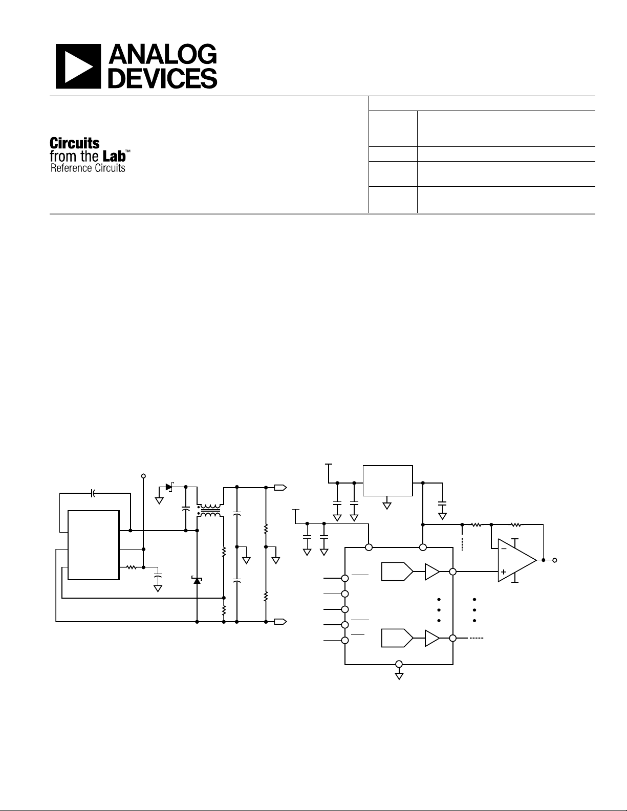
Precision 16-Bit, Bipolar Output Voltage Source with +12 V to ±5 V Supply
EVALUATION AND DESIGN SUPPORT
Circuit Evaluation Boards
CN-0183 Circuit Evaluation Board (EVAL-CN0183-SDZ)
System Demonstration Platform (EVAL-SDP-CB1Z)
Design and Integration Files
Schematics, Layout Files, Bill of Materials
CIRCUIT FUNCTION AND BENEFITS
The circuit shown in Figure 1 provides a precision 16-bit, low
drift bipolar voltage output of ±2.5 V and operates on a single
+10 V to +15 V supply. The unipolar voltage outputs of the
AD5668 octal denseDAC are amplified and level shifted by the
AD8638 auto-zero op amps. The maximum drift contribution
Circuit Note
Devices Connected/Referenced
16-Bit Voltage Output denseDAC with
AD5668
AD8638 16 V Auto-Zero, Rail-to-Rail Output Op Amp
ADP2300
REF192
of the AD8638 is only 0.06 ppm/°C. The external REF192 reference
ensures a maximum drift of 5 ppm/°C (E grade) and provides a
low impedance pseudo ground for the AD8638 level gain and
shifting circuit.
The circuit offers an efficient solution to a problem often
encountered in systems with a single +12 V supply rail. Proper
printed circuit board (PCB) layout and grounding techniques
ensure that the ADP2300 switching regulator does not degrade
the overall performance of the circuit.
5 ppm/°C On-Chip Reference and SPI
Interface
1.2 A, 20 V, 700 kHz, Nonsynchronous StepDown Switching Regulator
Precision Micropower, 2.5 V Low Dropout
Voltage Reference
Circuits from the Lab™ circuits from Analog Devices have been designed and built by Analog Devices
room
be liable for direct, indirect, special, incidental, cons
Figure 1. Bipolar Output DAC Circuit with ±5 V Power Supplies
One Technology Way, P.O. Box 9106, Norwood, MA 02062-9106, U.S.A.
Tel: 781.329.4700
www.analog.com
Page 2
CN-0183 Circuit Note
6
5
4
3
2
1
0
INL (LSB)
–1
–2
–3
–4
–5
0 10000 20000 30000
DAC CODE
40000 50000 60000
09471-002
0.6
0.4
0.2
0
DNL (LSB)
–0.2
–0.4
–0.8
–0.6
0 10000 20000 30000
DAC CODE
40000 50000 60000
09471-003
8
6
4
2
INL (LSB)
0
–2
–6
–4
0 10000 20000 30000
DAC CODE
40000 50000 60000
09471-004
0.8
0.6
0.4
0.2
0
–0.2
–0.4
DNL (LSB)
–0.6
–0.8
–1.0
0 10000 20000 30000
DAC CODE
40000 50000 60000
09471-005
CIRCUIT DESCRIPTION
The AD5668 is a 16-bit, octal, voltage output denseDAC
controlled by an SPI interface. It contains an on-chip reference
with a 10 ppm/°C maximum drift specification. The on-chip
reference is off at power-up, allowing the use of an external
reference. The internal reference is enabled via a software write.
In the circuit shown in Figure 1, an external REF192 is used
because a low output impedance is required to drive the 2.5 V
pseudo ground reference for the AD8638 op amps.
The output voltage of the AD5668 is 0 V to 2.5 V at TP1, and
this signal drives the noninverting input of the AD8638 op amp.
The signal gain of the op amp is 1 + R2/R1, which is 2 for R1 = R2.
A negative 2.5 V offset is injected into the op amp output by
driving R1 with the 2.5 V reference. The result is a bipolar
output voltage at TP2 that swings from −2.5 V to +2.5 V.
The circuit operates on a single supply voltage of nominally 12 V,
which can vary between 10 V and 15 V. The regulated −5 V
supply rail is developed from an ADP2300 switching regulator
connected in the inverting buck-boost configuration. The circuit
can be designed using the ADIsimPower program available at
www.analog.com/ADIsimPower. The L1 coupled inductor is
used to develop an unregulated 5 V supply for the circuit using
a Zeta configuration. This circuit yields high efficiency for small
output currents.
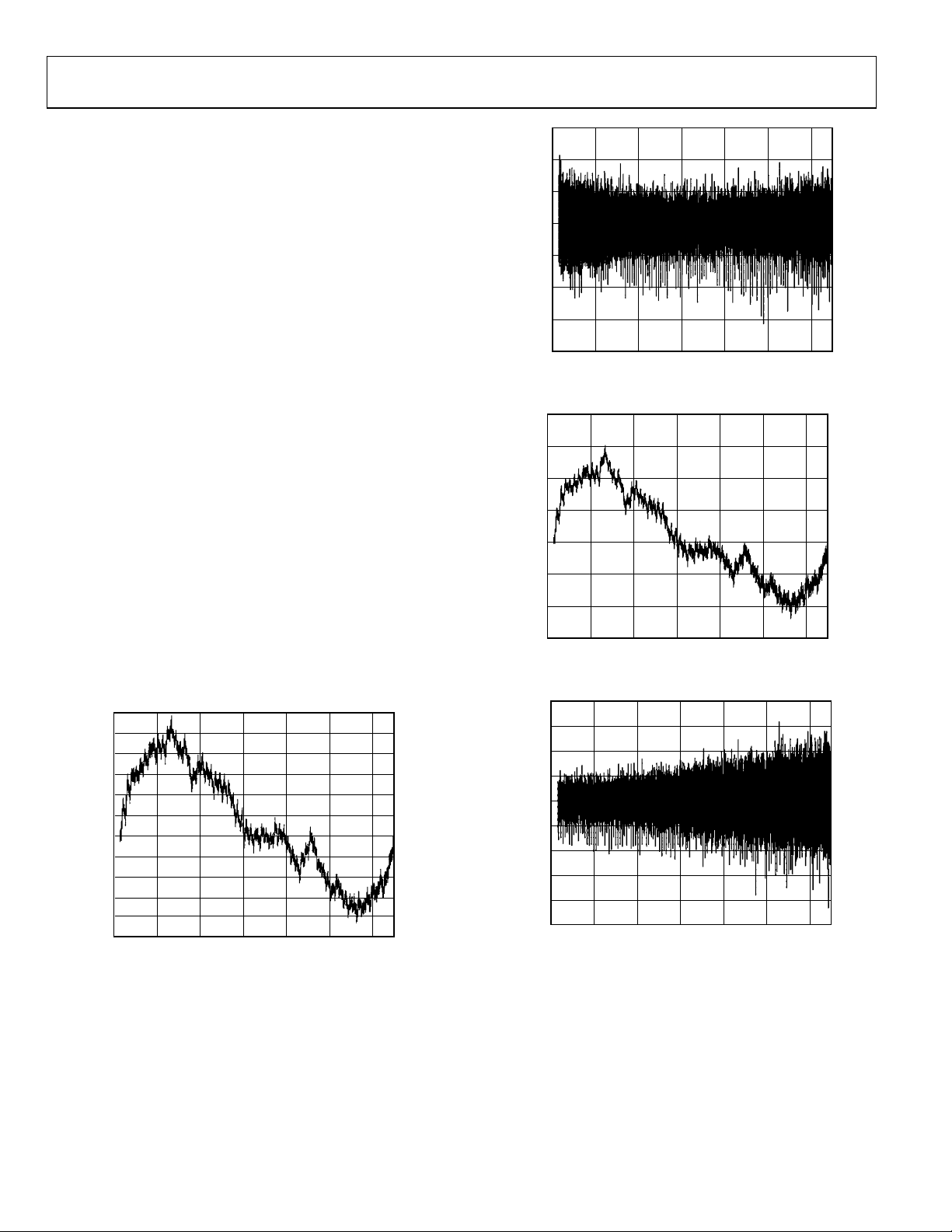
The integral nonlinearity (INL) and differential nonlinearity
(DNL) measured at TP2 (bipolar output) are shown in Figure 2
and Figure 3, respectively.
The INL and DNL measured at TP1 (unipolar DAC output) are
shown in Figure 4 and Figure 5, respectively.
Figure 3. DNL Performance of Bipolar Output (TP2)
Figure 4. INL Performance of Unipolar DAC Output (TP1)
Figure 2. INL Performance of Bipolar Output (TP2)
Rev. 0 | Page 2 of 5
Figure 5. DNL Performance of Unipolar DAC Output (TP1)
Page 3

Circuit Note CN-0183
09471-006
POWER SUPPLY
PC
EVAL-CN0183-SDZ
SDP
OSCILLOSCOPE
CON A
OR
CON B
USB
USB
+12V
AVDD AGND –5V
120-PIN SD P
J1
J4-1
J4-2
J5-1
J5-2 J5-3
DAC_OUT/TP1
BIPOLAR_OUT/TP2
+12V+5V GND GND
AGND
–5V
09471-007
COMMON VARIATIONS
The AD5628 and AD5648 are 12-bit and 14-bit versions of the
AD5668. All have an on-chip reference with an internal gain of 2.
The AD5628-1/AD5648-1/AD5668-1 have a 1.25 V, 5 ppm/°C
reference, giving a full-scale output range of 2.5 V; and the
AD5628-2/AD5648-2/AD5668-2 and AD5668-3 have a 2.5 V,
5 ppm/°C reference, giving a full-scale output range of 5 V. The
on-board reference is off at power-up, allowing the use of an
external reference. The internal reference is enabled via a software
write. The part incorporates a power-on-reset circuit that ensures
that the DAC output powers up to 0 V (AD5628-1/AD5648-1/
AD5668-1, AD5628-2/AD5648-2/AD5668-2) or midscale
(AD5668-3) and remains powered up at this level until a valid
write takes place.
The AD8639 is a dual version of the AD8638 and can be used, if
desired. The circuit in Figure 1 uses the single AD8638 to minimize
crosstalk between the eight channels.
Other 2.5 V references can be used, such as the ADR4525, which
has an accuracy of ±0.02% and a temperature coefficient of
2 ppm/°C maximum (B grade).
CIRCUIT EVALUATION AND TEST
Equipment Needed (Equivalents Can Be Substituted)
The following equipment is needed:
• The System Demonstration Platform (EVA L -SDP-CB1Z)
• The CN-0183 circuit evaluation board (EVA L-CN0183-SDZ)
• The CN-0183 evaluation software
• The Tektronix TDS2024, 4-channel oscilloscope
• The HP E3630A 0 V to 6 V/2.55 A; ±20 V/0.5 A triple
output dc power supply
• A PC (Windows 32-bit or 64-bit)
Getting Started
Load the evaluation software by placing the CN-0183 evaluation
software CD in the CD drive of the PC. Using My Computer,
locate the drive that contains the evaluation software CD and
open the Readme file. Follow the instructions contained in the
Readme file for installing and using the evaluation software.
The evaluation software main window is shown in Figure 6.
Figure 6. Evaluation Software Main Window
Functional Diagram of Test Setup
A functional diagram of the test setup is shown in Figure 7. This
setup allows the DAC output (TP1) and the bipolar output (TP2) to
be observed with an oscilloscope.
Linearity measurements require a precision, digital voltmeter
(DVM) that can be read by the PC via a USB port.
Figure 7. Functional Diagram of Test Setup
Rev. 0 | Page 3 of 5
Page 4

CN-0183 Circuit Note
LK2
AVDD supply source
Position A
The circuit is powered by an external 5 V supply applied to the AVDD
Setup
Connect the 120-pin connector on the E VA L-CN0183-SDZ to
the CON A connector or the CON B connector on the EVA L -
SDP-CB1Z. Use nylon hardware to firmly secure the two
boards, using the holes provided at the ends of the 120-pin
connectors. After successfully setting the dc output supply to
+5 V, −5 V, and +12 V, turn the power supply off.
With power to the supply off, connect the −5 V power supply to
the −5V pin on J5-3, connect the +5 V power supply to the
AVDD pin on J5-1, connect GND to the AGND pins on J5-2
and J4-2, and connect the +12 V power supply to the +12V pin
on J4-1. Alternatively, place Link 2 and Link 3 in Position B to
power the circuitry using the ADP2300 to supply +5 V and −5 V.
Note that AVD D a n d the −5 V are not needed in this case.
Turn on the power supply and then connect the USB cable from
the SDP board to the USB port on the PC. Do not connect the
USB cable to the mini-USB connector on the SDP before turning
on the dc power supply for the E VA L-CN0183-SDZ.
Table 1. Jumper Settings for EVAL-CN0183-SDZ (Default Settings in Bold)
Jumper Description Setting Function
LK1 Short AD5668 reference pin to
REF192 output
Opened Only the internal reference of the AD5668 can be used.
Inserted It shorts AD5668 reference pin to REF192 output allowing the use of an
external DAC reference.
After setting up the test equipment, connect the probes of the
oscilloscope to the TP1 and TP2 test points. The TP3, TP4, and
TP5 test points are connected to the reference, the regulated +5 V,
and the regulated −5 V, respectively. Check these test points for
the correct voltages (use TP6 for the ground).
The software provided on the CD allows users to set the value of
V
A by loading a code into the DAC and by choosing the source
OUT
of the reference. If users keep the default setting, they will have
to supply the +5 V and −5 V voltages, and the +12 V is not
required. The default setting uses the external REF192 reference,
giving you a full-scale DAC output range of 2.5 V (TP1), and
−2.5 V to +2.5 V on the bipolar output (TP2). Loading 0x0000
sets the DAC output to 0 V and the bipolar output to −2.5 V.
Loading 0x8000 sets the DAC output to 1.25 V and the bipolar
output to 0 V. Loading 0xFFFF sets the DAC output to 2.5 V
and the bipolar output to 2.5 V.
pin on J5-1.
Position B The digital power is supplied by the 5 V voltage supplied by the ADP2300
regulator.
LK5 −5 V voltage source
Position B The digital power is supplied by the −5 V voltage obtained by inverting the
Position A The analog circuit is supplied by an external power supply apply to the
−5V pin on J5-3.
output of the ADP2300 regulator.
Rev. 0 | Page 4 of 5
Page 5

Circuit Note CN-0183
(Continued from first page) Circuits from the L ab circuits are intended only for use with Analog Devices products and are the intellectual property of Analog Devices or its licensors. While you
reserves the right to change any Circuits from the Lab circuits at any time without notic e but is under no obligation to do so.
registered trademarks are the property of their respective owners.
LEARN MORE
CN-0183 Design Support Package:
http://www.analog.com/CN0183-DesignSupport
Ardizzoni, John. A Practical Guide to High-Speed Printed-
Circuit-Board Layout, Analog Dialogue 39-09, September
2005.
MT-031 Tutorial, Grounding Data Converters and Solving the
Mystery of “AGND” and “DGND”, Analog Devices.
MT-101 Tutorial, Decoupling Techniques, Analog Devices.
ADIsimPower Design Tool
Data Sheets and Evaluation Boards
CN-0183 Circuit Evaluation Board (EVAL-CN0183-SDZ)
System Demonstration Platform (EVAL-SDP-CB1Z)
AD5668 Data Sheet and Evaluation Board
AD8638 Data Sheet and Evaluation Board
ADP2300 Data Sheet and Evaluation Board
REF192 Data Sheet and Evaluation Board
REVISION HISTORY
6/12—Rev. 0: Initial Version
may use the Circuits from the Lab circuits in the design of your product, no other license is granted by implication or otherwise under any patents or other intellectual property by
application or use of the Circuits from the Lab circuits. Information furnished by Analog Devices is believed to be accurate and reliable. However, Circuits from the Lab circuits are supplied
"as is" and without warranties of any kind, express, implied, or statutory including, but not limited to, any implied warranty of merchantability, noninfringement or fitness for a particular
purpose an d no responsibil ity is assumed by Analog Device s for their use, nor for any infringements of patents or other rights of third parties that may result from their use. Analog Devices
©2012 Analog Devices, Inc. All rights reserved. Trademarks and
CN09471-0-6/12(0)
Rev. 0 | Page 5 of 5
 Loading...