

Page 1
CMX867
Low Power
V.22 Modem
2001 Consumer Microcircuits Limited
D/867/2 November 2001 Provisional Information
Features Applications
•• V.22, Bell 212A 1200/1200 or 600/600 bps DPSK •• Telephone Telemetry Systems
•• V.23 1200/75, 1200/1200, 75, 1200 bps FSK •• Remote Utility Meter Reading
•• Bell 202 1200/150, 1200/1200, 150, 1200 bps FSK •• Security Systems
•• V.21 or Bell 103 300/300 bps FSK •• Industrial Control Systems
•• DTMF/Tones Transmit and Receive •• Electronic Cash Terminals
•• ‘Powersave’ Standby Mode •• Pay-Phones
•• Software and Hardware Compatible with CMX868 •• Cable TV Set-Top Boxes
1.1 Brief Description
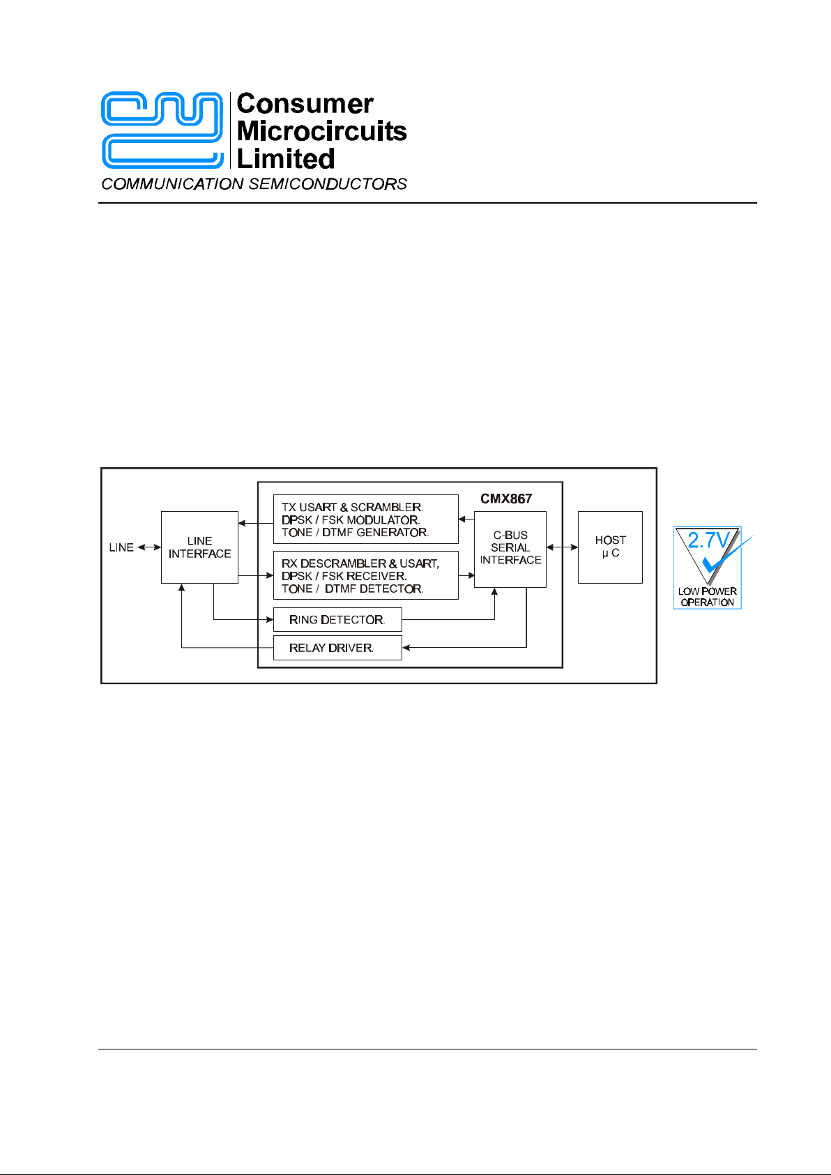
The CMX867 is a multi-standard modem for use in telephone based information and telemetry systems.
Control of the device is via a simple high speed serial bus, compatible with most types of µC serial
interface. The data transmitted and received by the modem is also transferred over the same serial bus.
On-chip programmable Tx and Rx USARTs meeting the requirements of V.14 are provided for use with
asynchronous data and allow unformatted synchronous data to be received or transmitted as 8-bit words.
It can transmit and detect standard DTMF and modem calling and answer signals or user-specific
programmed single or dual tone signals. A general purpose Call Progress signal detector is also included.
Flexible line driver and receive hybrid circuits are integrated on chip, requiring only passive external
components to build a 2 or 4-wire line interface.
The device also features a Hook Switch Relay Drive output and a Ring Detector circuit which continues
to function when the device is in the Powersave mode, providing an interrupt which can be used to wake
up the host µController when line voltage reversal or ringing is detected.
The CMX867 operates from a single 2.7 to 5.5V supply over a temperature range of -40°C to +85°C and
is available in 24-pin TSSOP, SOIC and DIP packages.
Page 2

Low Power V.22 Modem CMX867
2001 Consumer Microcircuits Limited 2 D/867/2
CONTENTS
Section Page
1.1 Brief Description..................................................................................1
1.2 Block Diagram .....................................................................................3
1.3 Signal List............................................................................................4
1.4 External Components..........................................................................5
1.4.1 Ring Detector Interface...........................................................6
1.4.2 Line Interface...........................................................................7
1.5 General Description.............................................................................9
1.5.1 Tx USART ..............................................................................10
1.5.2 FSK and DPSK Modulators ..................................................11
1.5.3 Tx Filter and Equaliser..........................................................12
1.5.4 DTMF/Tone Generator..........................................................12
1.5.5 Tx Level Control and Output Buffer.....................................12
1.5.6 Rx DTMF/Tones Detectors....................................................13
1.5.7 Rx Modem Filterering and Demodulation............................14
1.5.8 Rx Modem Pattern Detectors and Descrambler ..................15
1.5.9 Rx Data Register and USART ...............................................15
1.5.10 C-BUS Interface .....................................................................17
1.5.10.1 General Reset Command ..............................17
1.5.10.2 General Control Register..............................19
1.5.10.3 Transmit Mode Register ...............................21
1.5.10.4 Receive Mode Register.................................24
1.5.10.5 Tx Data Register............................................26
1.5.10.6 Rx Data Register ...........................................26
1.5.10.7 Status Register..............................................27
1.5.10.8 Programming Register..................................30
1.6 Application Notes..............................................................................34
1.6.1 V.22 Calling Modem Application..........................................34
1.6.2 V.22 Answering Modem Application....................................35
1.7 Performance Specification................................................................36
1.7.1 Electrical Performance..........................................................36
1.7.1.1 Absolute Maximum Ratings .....................................36
1.7.1.2 Operating Limits .......................................................36
1.7.1.3 Operating Characteristics........................................37
1.7.2 Packaging..............................................................................44
Page 3
Low Power V.22 Modem CMX867
2001 Consumer Microcircuits Limited 3 D/867/2
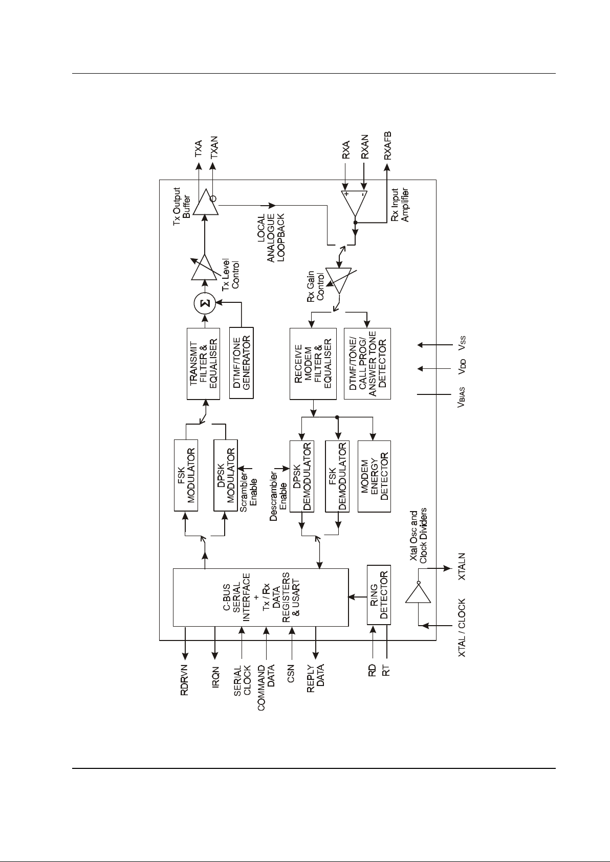
1.2 Block Diagram
Figure 1 Block Diagram
Page 4

Low Power V.22 Modem CMX867
2001 Consumer Microcircuits Limited 4 D/867/2
1.3 Signal List
CMX867
D2/E2/P4
Signal Description
Pin No. Name Type
1
XTALN O/P The output of the on-chip Xtal oscillator inverter.
2
XTAL/CLOCK I/P
The input to the oscillator inverter from the Xtal
circuit or external clock source.
3
RDRVN O/P
Relay drive output, low resistance pull down to
VSS when active and medium resistance pull up
to VDD when inactive.
4, 8, 12, 17, 21
VSS Power
The negative supply rail (ground).
5
RD I/P
Schmitt trigger input to the Ring signal detector.
Connect to VSS if Ring Detector not used.
6
RT BI
Open drain output and Schmitt trigger input
forming part of the Ring signal detector.
Connect to VDD if Ring Detector not used.
7, 16, 24
VDD Power The positive supply rail. Levels and thresholds
within the device are proportional to this
voltage.
9
RXAFB O/P The output of the Rx Input Amplifier.
10
RXAN I/P
The inverting input to the Rx Input Amplifier
11
RXA I/P
The non-inverting input to the Rx Input Amplifier
13
VBIAS O/P Internally generated bias voltage of
approximately VDD /2, except when the device
is in ‘Powersave’ mode when VBIAS will
discharge to VSS. Should be decoupled to VSS
by a capacitor mounted close to the device pins.
14
TXAN O/P
The inverted output of the Tx Output Buffer.
15
TXA O/P
The non-inverted output of the Tx Output Buffer.
18
CSN I/P
The C-BUS chip select input from the µC.
19
COMMAND
DATA
I/P
The C-BUS serial data input from the µC.
20
SERIAL
CLOCK
I/P
The C-BUS serial clock input from the µC.
22
REPLY DATA T/S
A 3-state C-BUS serial data output to the µC.
This output is high impedance when not sending
data to the µC.
23
IRQN O/P
A ‘wire-ORable’ output for connection to a µC
Interrupt Request input. This output is pulled
down to VSS when active and is high impedance
when inactive. An external pullup resistor is
required ie R1 of Figure 2.
Page 5
Low Power V.22 Modem CMX867
2001 Consumer Microcircuits Limited 5 D/867/2
Notes:
I/P = Input
O/P = Output
BI = Bidirectional
T/S = 3-state Output
NC = No Connection
1.4 External Components
R1
100kΩ
C1, C2 22pF
X1 11.0592MHz C3, C4 100nF
or 12.288MHz C5 10uF
Resistors ±5%, capacitors ±20% unless otherwise stated.
Figure 2 Recommended External Components for Typical Application
This device is capable of detecting and decoding small amplitude signals. To achieve this VDD and
VBIAS should be decoupled and the receive path protected from extraneous in-band signals. It is
recommended that the printed circuit board is laid out with a VSS ground plane in the CMX867 area to
provide a low impedance connection between the VSS pins and the VDD and VBIAS decoupling capacitors.
The VSS connections to the Xtal oscillator capacitors C1 and C2 should also be low impedance and
preferably be part of the VSS ground plane to ensure reliable start up of the oscillator.
For best results, an Xtal oscillator design should drive the clock inverter input with signal levels of at least
40% of VDD peak-to-peak. Tuning-fork Xtals generally cannot meet this requirement. To obtain Xtal
oscillator design assistance, please consult your Xtal manufacturer.
Page 6
Low Power V.22 Modem CMX867
2001 Consumer Microcircuits Limited 6 D/867/2
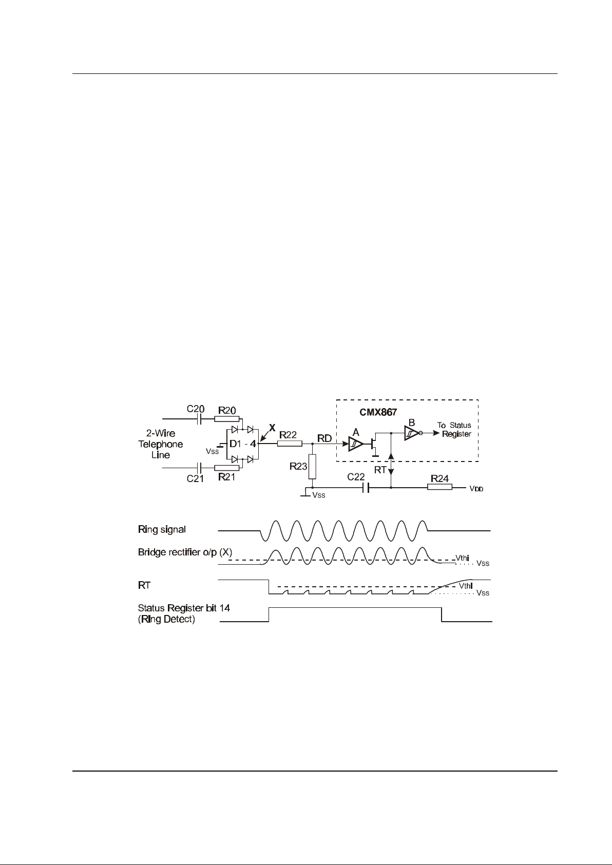
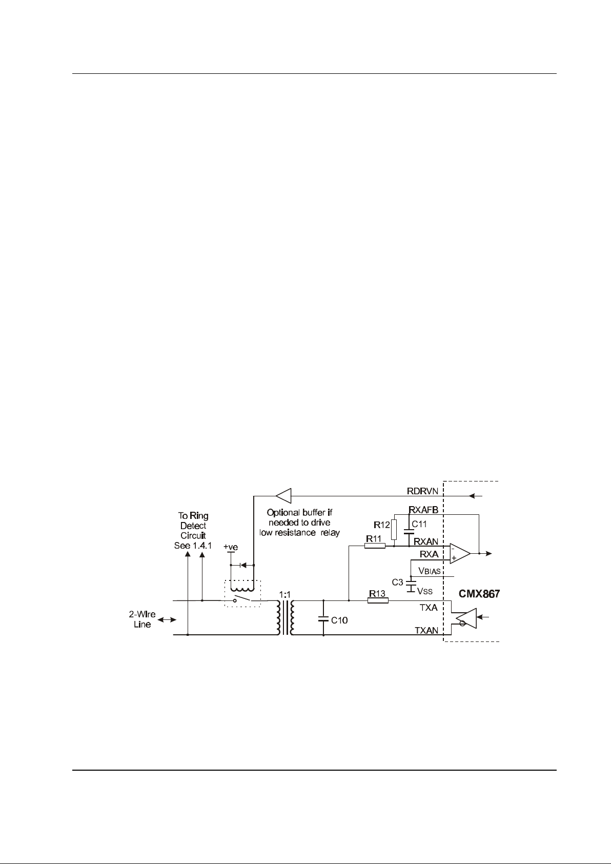
1.4.1 Ring Detector Interface
Figure 3 shows how the CMX867 may be used to detect the large amplitude Ringing signal voltage
present on the 2-wire line at the start of an incoming telephone call.
The ring signal is usually applied at the subscriber's exchange as an ac voltage inserted in series with
one of the telephone wires and will pass through either C20 and R20 or C21 and R21 to appear at the top
end of R22 (point X in Figure 3) in a rectified and attenuated form.
The signal at point X is further attenuated by the potential divider formed by R22 and R23 before being
applied to the CMX867 RD input. If the amplitude of the signal appearing at RD is greater than the input
threshold (Vthi) of Schmitt trigger 'A' then the N transistor connected to RT will be turned on, pulling the
voltage at RT to VSS by discharging the external capacitor C22. The output of the Schmitt trigger 'B' will
then go high, setting bit 14 (Ring Detect) of the Status Register.
The minimum amplitude ringing signal that is certain to be detected is:
( 0.7 + Vthi x [R20 + R22 + R23] / R23 ) x 0.707 Vrms
where Vthi is the high-going threshold voltage of the Schmitt trigger A (see section 1.7.1).
With R20-22 all 470kΩ as Figure 3, then setting R23 to 68kΩ will guarantee detection of ringing signals
of 40Vrms and above for VDD over the range 3 to 5V.
R20, 21, 22
470kΩ
C20, 21
0.1µF
R23 See text C22
0.33µF
R24
470kΩ
D1-4 1N4004
Resistors ±5%, capacitors ±20%
Figure 3 Ring Signal Detector Interface Circuit
Page 7
Low Power V.22 Modem CMX867
2001 Consumer Microcircuits Limited 7 D/867/2
If the time constant of R24 and C22 is large enough then the voltage on RT will remain below the
threshold of the 'B' Schmitt trigger for the duration of a ring cycle.
The time for the voltage on RT to charge from VSS towards VDD can be derived from the formula
VRT = V
DD
x [1 - exp(-t/(R24 x C22)) ]
As the Schmitt trigger high-going input threshold voltage (Vthi) has a minimum value of 0.56 x VDD, then
the Schmitt trigger B output will remain high for a time of at least 0.821 x R24 x C22 following a pulse at
RD.
The values of R24 and C22 given in Figure 3 (470kΩ and 0.33µF) give a minimum RT charge time of
100 msec, which is adequate for ring frequencies of 10Hz or above.
Note that the circuit will also respond to a telephone line voltage reversal. If necessary the µC can
distinguish between a Ring signal and a line voltage reversal by measuring the time that bit 14 of the
Status Register (Ring Detect) is high.
If the Ring detect function is not used then pin RD should be connected to VSS and RT to VDD.
1.4.2 Line Interface
A line interface circuit is needed to provide dc isolation and to terminate the line.
2-Wire Line Interface
Figure 4a shows an interface for use with a 600Ω 2-wire line. The complex line termination is provided by
R13 and C10, high frequency noise is attenuated by C10 and C11, while R11 and R12 set the receive
signal level into the modem. For clarity the 2-wire line protection circuits have not been shown.
R11 See text C3 See Figure 2
R12
100kΩ
C10 33nF
R13
600Ω
C11 100pF
Resistors ±5%, capacitors ±20%
Figure 4a 2-Wire Line Interface Circuit
Page 8
Low Power V.22 Modem CMX867
2001 Consumer Microcircuits Limited 8 D/867/2
The transmit line signal level is determined by the voltage swing between the TXA and TXAN pins, less
6dB due to the line termination resistor R13, and less the loss in the line coupling transformer.
Allowing for 1dB loss in the transformer, then with the Tx Mode Register set for a Tx Level Control gain
of 0dB the nominal transmit line levels will be:
VDD = 3.0V VDD = 5.0V
DPSK and FSK Tx modes (no guard tone) -10dBm -5.5dBm
Single tone transmit mode -10dBm -5.5dBm
DTMF transmit mode -6 and -8 dBm -1.5 and -3.5 dBm
For a line impedance of 600Ω, 0dBm = 775mVrms. See also section 1.7.1.3
In the receive direction, the signal detection thresholds within the CMX867 are proportional to VDD and
are affected by the Rx Gain Control gain setting in the Rx Mode Register. The signal level into the
CMX867 is affected by the line coupling transformer loss and the values of R11 and R12 of Figure 4a.
Assuming 1dB transformer loss, the Rx Gain Control programmed to 0dB and R12 = 100kΩ, then for
correct operation (see section 1.7.1.3) the value of R11 should be equal to 500 / VDD kΩ i.e. 160kΩ at
3.0V, falling to 100kΩ at 5.0V
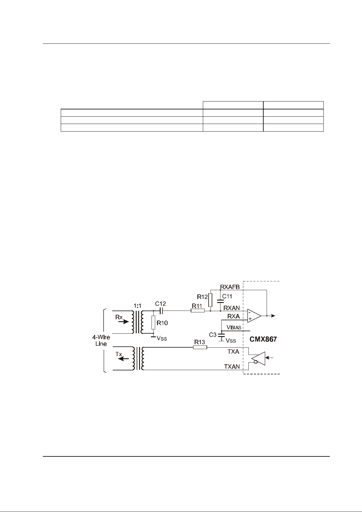
4-Wire Line Interface
Figure 4b shows an interface for use with a 600Ω 4-wire line. The line terminations are provided by R10
and R13, high frequency noise is attenuated by C11 while R11 and R12 set the receive signal level into
the modem.
Transmit and receive line level settings and the value of R11 are as for the 2-wire circuit.
R10, 13
600Ω
C3 See Figure 2
R11 See text C11 100pF
R12
100kΩ
C12 33nF
Resistors ±5%, capacitors ±20%
Figure 4b 4-Wire Line Interface Circuit
Page 9

Low Power V.22 Modem CMX867
2001 Consumer Microcircuits Limited 9 D/867/2
1.5 General Description
The CMX867 transmit and receive operating modes are independently programmable.
The transmit mode can be set to any one of the following:
V.22 and Bell 212A modem. 1200 or 600 bps DPSK (Differential Phase Shift Keying).
V.21 modem. 300bps FSK (Frequency Shift Keying).
Bell 103 modem. 300bps FSK.
V.23 modem. 1200 or 75 bps FSK.
Bell 202 modem. 1200 or 150 bps FSK.
DTMF transmit.
Single tone transmit (from a range of modem calling, answer and other tone frequencies)
User programmed tone or tone pair transmit (programmable frequencies and levels)
Disabled.
The receive mode can be set to any one of the following:
V.22 and Bell 212A modem. 1200 or 600 bps DPSK.
V.21 modem. 300bps FSK.
Bell 103 modem. 300 bps FSK.
V.23 modem. 1200 or 75 bps FSK.
Bell 202 modem. 1200 or 150 bps FSK.
DTMF detect.
2100Hz and 2225Hz answer tone detect.
Call progress signal detect.
User programmed tone or tone pair detect.
Disabled.
The CMX867 may also be set into a Powersave mode which disables all circuitry except for the C-BUS
interface and the Ring Detector.
Page 10
Low Power V.22 Modem CMX867
2001 Consumer Microcircuits Limited 10 D/867/2
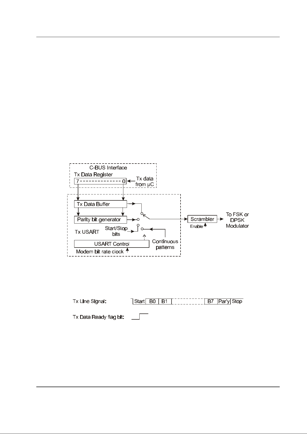
1.5.1 Tx USART
A flexible Tx USART is provided for all modem modes, meeting the requirements of V.14 for DPSK
modems.
It can be programmed to transmit continuous patterns, Start-Stop characters or Synchronous Data.
In both Synchronous Data and Start-Stop modes the data to be transmitted is written by the µC into the
8-bit C-BUS Tx Data Register from which it is transferred to the Tx Data Buffer.
If Synchronous Data mode has been selected the 8 data bits in the Tx Data Buffer are transmitted
serially, b0 being sent first.
In Start-Stop mode a single Start bit is transmitted, followed by 5, 6, 7 or 8 data bits from the Tx Data
Buffer - b0 first - followed by an optional Parity bit then - normally - one or two Stop bits. The Start, Parity
and Stop bits are generated by the USART as determined by the Tx Mode Register settings and are not
taken from the Tx Data Register.
Figure 5a Tx USART
Every time the contents of the C-BUS Tx Data Register are transferred to the Tx Data Buffer the Tx Data
Ready flag bit of the Status Register is set to 1 to indicate that a new value should be loaded into the CBUS Tx Data Register. This flag bit is cleared to 0 when a new value is loaded into the Tx Data Register.
Figure 5b Tx USART Function (Start-Stop mode, 8 Data Bits + Parity)
If a new value is not loaded into the Tx Data Register in time for the next Tx Data Register to Tx Data
Buffer transfer then the Status Register Tx Data Underflow bit will be set to 1. In this event the contents
of the Tx Data Buffer will be re-transmitted if Synchronous Data mode has been selected, or if the Tx
modem is in Start-Stop mode then a continuous Stop signal (1) will be transmitted until a new value is
loaded into the Tx Data Register.
Page 11

Low Power V.22 Modem CMX867
2001 Consumer Microcircuits Limited 11 D/867/2
In all modes the transmitted bit and baud rates are the nominal rates for the selected modem type, with
an accuracy determined by the XTAL frequency accuracy, however for DPSK modes V.14 requires that
Start-Stop characters can be transmitted at up to 1% overspeed (basic signalling rate range) or 2.3%
overspeed (extended signalling rate range) by deleting a Stop bit from no more than one out of every 8
(basic range) or 4 (extended range) consecutive transmitted characters.
To accommodate the V.14 requirement the Tx Data Register has been given two C-BUS addresses, $E3
and $E4. Data should normally be written to $E3.
In DPSK Start-Stop modes if data is written to $E4 then the programmed number of Stop bits will be
reduced by one for that character. In this way the µC can delete transmitted Stop bits as needed.
In FSK Start-Stop modes, data written to $E4 will be transmitted with a 12.5% reduction in the length of
the Stop bit at the end of that character.
In all Synchronous Data modes data written to $E4 will be treated as though it had been written to $E3.
The underspeed transmission requirement of V.14 is automatically met by the CMX867 as in Start-Stop
mode it automatically inserts extra Stop bit(s) if it has to wait for new data to be loaded into the C-BUS
Tx Data Register.
The optional V.22 compatible data scrambler can be programmed to invert the next input bit in the event
of 64 consecutive ones appearing at its input. It uses the generating polynomial:
1 + x
-14
+ x
-17
1.5.2 FSK and DPSK Modulators
Serial data from the USART is fed via the optional scrambler to the FSK modulator if V.21, V.23, Bell
103 or Bell 202 mode has been selected or to the DPSK modulator for V.22 and Bell 212A modes.
The FSK modulator generates one of two frequencies according to the transmit mode and the value of
current transmit data bit.
The DPSK modulator generates a carrier of 1200Hz (Low Band, Calling modem) or 2400Hz (High Band,
Answering modem) which is modulated at 600 symbols/sec as described below:
600bps V.22 signals are transmitted as a +90° carrier phase change for a ‘0’ bit, +270° for ‘1’.
For V.22 and Bell 212A 1200bps DPSK the transmit data stream is divided into groups of two
consecutive bits (dibits) which are encoded as a carrier phase change:
Dibit
(left-hand bit is the
first of the pair)
Phase change
00
+90°
01
0°
11
+270°
10
+180°
Page 12

Low Power V.22 Modem CMX867
2001 Consumer Microcircuits Limited 12 D/867/2
1.5.3 Tx Filter and Equaliser
The FSK or DPSK modulator output signal is fed through the Transmit Filter and Equaliser block which
limits the out-of-band signal energy to acceptable limits. In 600 and 1200 bps FSK and DPSK modes this
block includes a fixed compromise line equaliser which is automatically set for the particular modulation
type and frequency band being employed. This fixed compromise line equaliser may be enabled or
disabled by bit 10 of the General Control Register. The amount of Tx equalisation provided compensates
for one quarter of the relative amplitude and delay distortion of ETS Test Line 1 over the frequency band
used.
1.5.4 DTMF/Tone Generator
In DTMF/Tones mode this block generates DTMF signals or single or dual frequency tones. In DPSK
modem modes it is used to generate the optional 550 or 1800Hz guard tone.
1.5.5 Tx Level Control and Output Buffer
The outputs (if present) of the Transmit Filter and DTMF/Tone Generator are summed then passed
through the programmable Tx Level Control and Tx Output Buffer to the pins TXA and TXAN. The Tx
Output Buffer has symmetrical outputs to provide sufficient line voltage swing at low values of VDD and
to reduce harmonic distortion of the signal.
Page 13
Low Power V.22 Modem CMX867
2001 Consumer Microcircuits Limited 13 D/867/2
1.5.6 Rx DTMF/Tones Detectors
In Rx Tones Detect mode the received signal, after passing through the Rx Gain Control block, is fed to
the DTMF / Tones / Call Progress / Answer Tone detector. The user may select any of four separate
detectors:
The DTMF detector detects standard DTMF signals. A valid DTMF signal will set bit 5 of the Status
Register to 1 for as long as the signal is detected.
The programmable tone pair detector includes two separate tone detectors (see Figure 11). The first
detector will set bit 6 of the Status Register for as long as a valid signal is detected, the second detector
sets bit 7, and bit 10 of the Status Register will be set when both tones are detected.
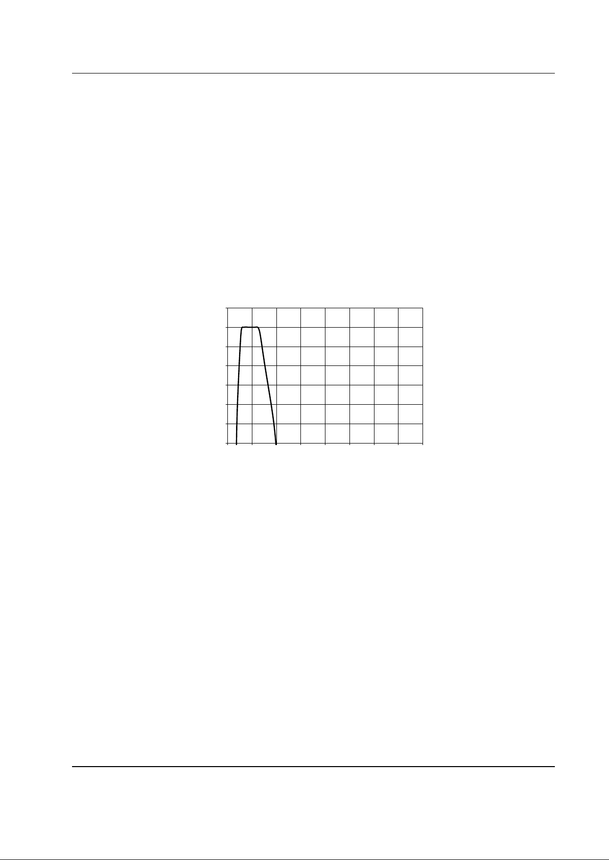
The Call Progress detector measures the amplitude of the signal at the output of a 275 - 665 Hz
bandpass filter and sets bit 10 of the Status Register to 1 when the signal level exceeds the
measurement threshold.
-60
-50
-40
-30
-20
-10
0
10
0 0.5 1 1.5 2 2.5 3 3.5 4
kHz
dB
Figure 6a Response of Call Progress Filter
The Answer Tone detector measures both amplitude and frequency of the received signal and sets bit 6
or bit 7 of the Status Register when a valid 2225Hz or 2100Hz signal is received.
Page 14
Low Power V.22 Modem CMX867
2001 Consumer Microcircuits Limited 14 D/867/2
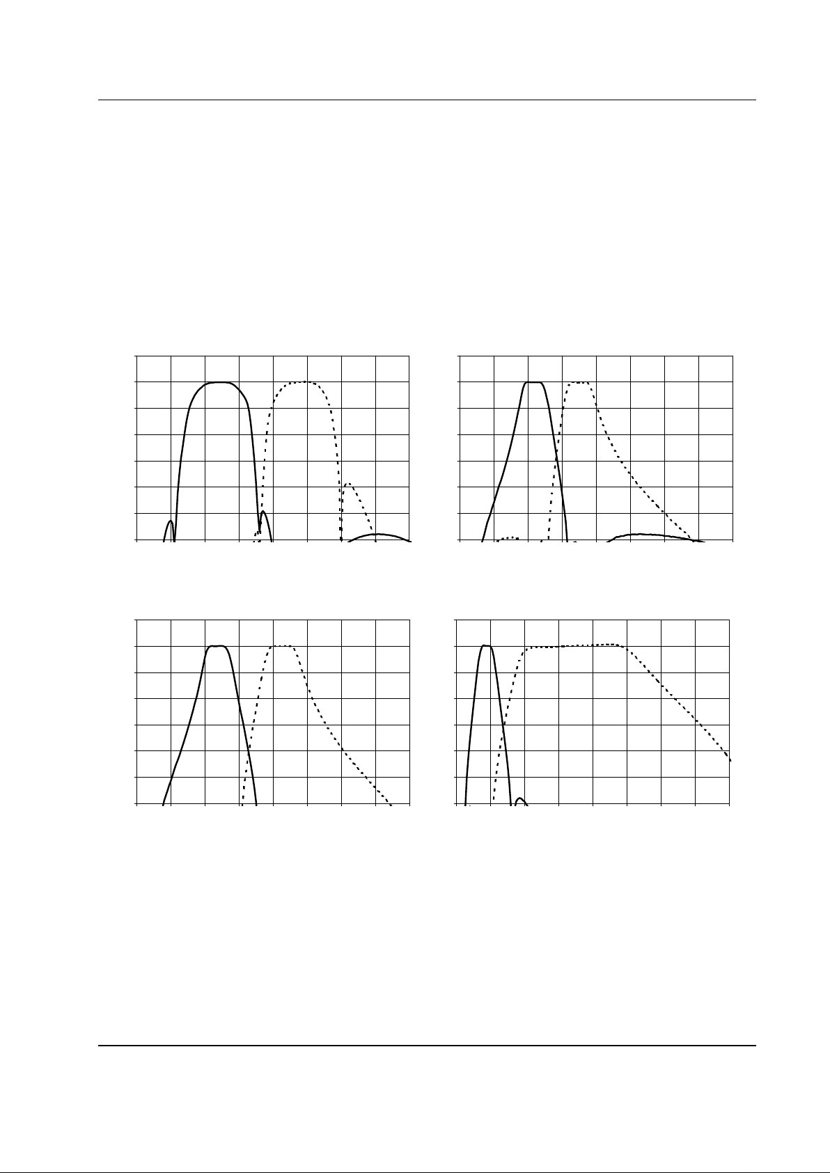
1.5.7 Rx Modem Filterering and Demodulation
When the receive part of the CMX867 is operating as a modem, the received signal is fed to a bandpass
filter to attenuate unwanted signals and to provide fixed compromise line equalisation for 600 and
1200bps FSK and DPSK modes. The characteristics of the bandpass filter and equaliser are determined
by the chosen receive modem type and frequency band. The line equaliser may be enabled or disabled
by bit 10 of the General Control Register and compensates for one quarter of the relative amplitude and
delay distortion of ETS Test Line 1.
The responses of these filters, including the line equaliser and the effect of external components used in
Figures 4a and 4b, are shown in Figures 6b-e:
-60
-50
-40
-30
-20
-10
0
10
0 0.5 1 1.5 2 2.5 3 3.5 4
kHz
dB
-60
-50
-40
-30
-20
-10
0
10
0 0.5 1 1.5 2 2.5 3 3.5 4
kHz
dB
Figure 6b DPSK Rx Filters Figure 6c V.21 Rx Filters
-60
-50
-40
-30
-20
-10
0
10
0 0.5 1 1.5 2 2.5 3 3.5 4
kHz
dB
-60
-50
-40
-30
-20
-10
0
10
0 0.5 1 1.5 2 2.5 3 3.5 4
kHz
dB
Figure 6d Bell 103 Rx Filters Figure 6e V.23/Bell 202 Rx Filters
The signal level at the output of the Receive Modem Filter and Equaliser is measured in the Modem
Energy Detector block, compared to a threshold value, and the result controls bit 10 of the Status
Register.
The output of the Receive Modem Filter and Equaliser is also fed to the FSK or DPSK demodulator
depending on the selected modem type.
Page 15

Low Power V.22 Modem CMX867
2001 Consumer Microcircuits Limited 15 D/867/2
The FSK demodulator recognises individual frequencies as representing received ‘1’ or ‘0’ data bits:
The DPSK demodulator decodes DPSK modulation of a 1200Hz or 2400Hz carrier and is used for V.22
and Bell 212A modes. It includes an adaptive receive signal equaliser (auto-equaliser) that will
automatically compensate for a wide range of line conditions in DPSK modes. The auto-equaliser can
provide a useful improvement in performance in 600 or 1200bps DPSK modes, so although it must be
disabled at the start of a handshake sequence, it can be enabled as soon as scrambled 1200bps 1s have
been detected.
Both FSK and DPSK demodulators produce a serial data bit stream which is fed to the Rx pattern
detector, descrambler and USART block, see Figure 7a. The demodulator input is also monitored for
continuous dibits '00,11' in 1200bps DPSK mode and continuous alternating 1s and 0s in all other modes.
The DPSK demodulator also estimates the received bit error rate by comparing the actual received signal
against an ideal waveform. This estimate is placed in bits 2-0 of the Status Register, see Figure 10.
1.5.8 Rx Modem Pattern Detectors and Descrambler
See Figure 7a.
The 1010.. pattern detector operates only in FSK modes and will set bit 9 of the Status Register when 32
bits of alternating 1’s and 0’s have been received.
The ‘Continuous Unscrambled 1’s’ detector operates in all modem modes and sets bits 8 and 7 of the
Status Register to ‘01’ when 32 consecutive 1’s have been received.
The descrambler operates only in DPSK modes and is enabled by setting bit 7 of the Rx Mode Register.
The ‘Continuous Scrambled 1’s’ detector operates only in DPSK modes when the descrambler is enabled
and sets bits 8 and 7 of the Status Register to ‘11’ when 32 consecutive 1’s appear at the output of the
descrambler. To avoid possible ambiguity, the ‘Scrambled 1’s’ detector is disabled when continuous
unscrambled 1’s are detected.
The ‘Continuous 0’s’ detector sets bits 8 and 7 of the Status Register to ‘10’ when NX consecutive 0’s
have been received, NX being 32 except when DPSK Start-Stop mode has been selected, in which case
NX = 2N + 4 where N is the number of bits per character including the Start, Stop and any Parity bits.
All of these pattern detectors will hold the ‘detect’ output for 12 bit times after the end of the detected
pattern unless the received bit rate or operating mode is changed, in which case the detectors are reset
within 2 msec.
1.5.9 Rx Data Register and USART
A flexible Rx USART is provided for all modem modes, meeting the requirements of V.14 for DPSK
modems. It can be programmed to treat the received data bit stream as Synchronous data or as StartStop characters.
In Synchronous mode the received data bits are all fed into the Rx Data Buffer which is copied into the
C-BUS Rx Data Register after every 8 bits.
In Start-Stop mode the USART Control logic looks for the start of each character, then feeds only the
required number of data bits (not parity) into the Rx Data Buffer. The parity bit (if used) and the presence
of a Stop bit are then checked and the data bits in the Rx Data Buffer copied to the C-BUS Rx Data
Register.
Page 16

Low Power V.22 Modem CMX867
2001 Consumer Microcircuits Limited 16 D/867/2
Figure 7a Rx Modem Data Paths
Whenever a new character is copied into the C-BUS Rx Data Register, the Rx Data Ready flag bit of the
Status Register is set to ‘1’ to prompt the µC to read the new data and, in Start-Stop mode, the Even Rx
Parity flag bit of the Status Register is updated.
In Start-Stop mode, if the Stop bit is missing (received as a ‘0’ instead of a ‘1’) the received character will
still be placed into the Rx Data Register and the Rx Data Ready flag bit set, but, unless allowed by the
V.14 overspeed option described below, the Status Register Rx Framing Error bit will also be set to ‘1’
and the USART will re-synchronise onto the next ‘1’ – ‘0’ (Stop – Start) transition. The Rx Framing Error
bit will remain set until the next character has been received.
Figure 7b Rx USART Function (Start-Stop mode, 8 Data Bits + Parity)
If the µC has not read the previous data from the Rx Data Register by the time that new data is copied to
it from the Rx Data Buffer then the Rx Data Overflow flag bit of the Status Register will be set to 1.
The Rx Data Ready flag and Rx Data Overflow bits are cleared to 0 when the Rx Data Register is read
by the µC.
For DPSK Start-Stop modes, V.14 requires that the receive USART be able to cope with missing Stop
bits; up to 1 missing Stop bit in every 8 consecutive received characters being allowed for the +1%
overspeed (basic signalling rate) V.14 mode and 1 in 4 for the +2.3% overspeed (extended signalling
rate) mode.
To accommodate the requirements of V.14, the CMX867 Rx Mode Register can be set for 0, +1% or
+2.3% overspeed operation in DPSK Start-Stop modes. Missing Stop bits beyond those allowed by the
selected overspeed option will set the Rx Framing Error flag bit of the Status Register.
Page 17

Low Power V.22 Modem CMX867
2001 Consumer Microcircuits Limited 17 D/867/2
In order that received Break signals can be handled correctly in V.14 Rx overspeed mode, a received
character which has all bits ‘0’, including the Stop and any Parity bits, will always cause the Rx Framing
Error bit to be set and the USART to re-synchronise onto the next ‘1’ – ‘0’ transition. Additionally the
received Continuous 0s detector will respond when more than 2M + 3 consecutive ‘0’s are received,
where ‘M’ is the selected total number of bits per character including Stop and any Parity bits.
1.5.10 C-BUS Interface
This block provides for the transfer of data and control or status information between the CMX867’s
internal registers and the µC over the C-BUS serial bus. Each transaction consists of a single Register
Address byte sent from the µC which may be followed by a one or more data byte(s) sent from the µC to
be written into one of the CMX867’s Write Only Registers, or a one or more byte(s) of data read out from
one of the CMX867’s Read Only Registers, as illustrated in Figure 8.
Data sent from the µC on the Command Data line is clocked into the CMX867 on the rising edge of the
Serial Clock input. Reply Data sent from the CMX867 to the µC is valid when the Serial Clock is high.
The CSN line must be held low during a data transfer and kept high between transfers. The C-BUS
interface is compatible with most common µC serial interfaces and may also be easily implemented with
general purpose µC I/O pins controlled by a simple software routine. Figure 14 gives detailed C-BUS
timing requirements.
The following C-BUS addresses and registers are used by the CMX867:
General Reset Command (address only, no data). Address $01
General Control Register, 16-bit write only. Address $E0
Transmit Mode Register, 16-bit write-only. Address $E1
Receive Mode Register, 16-bit write-only. Address $E2
Transmit Data Register, 8-bit write only. Addresses $E3 and $E4
Receive Data Register, 8-bit read-only. Address $E5
Status Register, 16-bit read-only. Address $E6
Programming Register, 16-bit write-only. Address $E8
Note: The C-BUS addresses $E9, $EA and $EB are allocated for production testing and should not be
accessed in normal operation.
1.5.10.1 General Reset Command
General Reset Command (no data) C-BUS address $01
This command resets the device and clears all bits of the General Control , Transmit Mode and Receive
Mode Registers and bits 15 and 13-0 of the Status Register.
Whenever power is applied to the CMX867 a General Reset command should be sent to the device, after
which the General Control Register should be set as required.
Page 18

Low Power V.22 Modem CMX867
2001 Consumer Microcircuits Limited 18 D/867/2
Figure 8 C-BUS Transactions
Page 19

Low Power V.22 Modem CMX867
2001 Consumer Microcircuits Limited 19 D/867/2
1.5.10.2 General Control Register
General Control Register: 16-bit write-only. C-BUS address $E0
This register controls general features of the CMX867 such as the Powersave and Loopback modes, the
IRQ mask bits and the Relay Drive output. It also allows the fixed compromise equalisers in the Tx and
Rx signal paths to be disabled if desired, and sets the internal clock dividers to use either a 11.0592 or a
12.288 MHz XTAL frequency.
All bits of this register are cleared to 0 by a General Reset command.
Bit:
15 14 13 12 11 10 9 8 7 6 5 4 3 2 1 0
0 0 0 Xtal
freq
LB Equ Rly
drv
Pwr Rst Irqn
en
IRQ Mask Bits
General Control Register b15-13: Reserved, set to 000
General Control Register b12: Xtal frequency
This bit should be set according to the Xtal frequency.
b12 = 1 11.0592MHz
b12 = 0 12.2880MHz
General Control Register b11: Analogue Loopback test mode
This bit controls the analogue loopback test mode. Note that in loopback test mode both
Transmit and Receive Mode Registers should be set to the same modem type and band or bit
rate.
b11 = 1 Local analogue loopback mode enabled
b11 = 0 No loopback (normal modem operation)
General Control Register b10: Tx and Rx Fixed Compromise Equalisers
This bit allows the Tx and Rx fixed compromise equalisers in the modem transmit and receive
filter blocks to be disabled.
b10 = 1 Disable equalisers
b10 = 0 Enable equalisers (600 or 1200bps modem modes)
General Control Register b9: Relay Drive
This bit directly controls the RDRVN output pin.
b9 = 1 RDRVN output pin pulled to VSS
b9 = 0 RDRVN output pin pulled to VDD
Page 20

Low Power V.22 Modem CMX867
2001 Consumer Microcircuits Limited 20 D/867/2
General Control Register b8: Powerup
This bit controls the internal power supply to most of the internal circuits, including the Xtal
oscillator and VBIAS supply. Note that the General Reset command clears this bit, putting the
device into Powersave mode.
b8 = 1 Device powered up normally
b8 = 0 Powersave mode (all circuits except Ring Detect, RDRVN and C-BUS
interface disabled)
When the power is first applied to the device, the following powerup procedure should be
followed to ensure correct operation.
i. (Power is applied to the device)
ii. Issue a General Reset command
iii. Write to the General Control Register (address $E0) setting both the Powerup bit
(b8) and the Reset bit (b7) to 1 – leave in this state for a minimum of about 20ms –
it is required that the crystal initially runs for this time in order to clock the internal
logic into a defined state. The device is now powered up, with the crystal and V
BIAS
supply operating, but is otherwise not running any transmit or receive functions.
iv. The device is now ready to be programmed as and when required. Examples:
• A General Reset command could be issued to clear all the registers and
therefore powersave the device.
• The Reset bit in the General Control Register could be set to 0 as part of a
routine to program all the relevant registers for setting up a particular operating
mode.
When the device is switched from Powersave mode to normal operation by setting the
Powerup bit to 1, the Reset bit should also be set to 1 and should be held at 1 for about 20ms
while the internal circuits, Xtal oscillator and V
BIAS
stabilise before starting to use the transmitter
or receiver.
General Control Register b7: Reset
Setting this bit to 1 resets the CMX867’s internal circuitry, clearing all bits of the Transmit and
Receive Mode Registers and b15 and b13-0 of the Status Register.
b7 = 1 Internal circuitry in a reset condition.
b7 = 0 Normal operation
General Control Register b6: IRQNEN (IRQN O/P Enable)
Setting this bit to 1 enables the IRQN output pin.
b6 = 1 IRQN pin driven low (to VSS) if the IRQ bit of the Status Register = 1
b6 = 0 IRQN pin disabled (high impedance)
General Control Register b5-0: IRQ Mask bits
These bits affect the operation of the IRQ bit of the Status Register as described in section
1.5.10.7
Page 21

Low Power V.22 Modem CMX867
2001 Consumer Microcircuits Limited 21 D/867/2
1.5.10.3 Transmit Mode Register
Transmit Mode Register: 16-bit write-only. C-BUS address $E1
This register controls the CMX867 transmit signal type and level. All bits of this register are cleared to 0
by a General Reset command, in Powersave mode, or when b7 (Reset) of the General Control Register
is 1.
Bit:
15 14 13 12 11 10 9 8 7 6 5 4 3 2 1 0
Tx mode = modem Tx level Guard tone Scrambler Start-stop /
synch data
# data bits /
synch data source
Tx mode = DTMF/Tones Tx level Unused, set to 0000 DTMF or Tone select
Tx mode = Disabled Set to 0000 0000 0000
Tx Mode Register b15-12: Tx mode
These 4 bits select the transmit operating mode.
b15 b14 b13 b12
1 1 1 1 Transmitter disabled (Reserved for future use)
1 1 1 0 Transmitter disabled (Reserved for future use)
1 1 0 1 V.22/Bell 212A 1200 bps DPSK High band (Answering modem)
1 1 0 0 “ Low band (Calling modem)
1 0 1 1 V.22 600 bps DPSK High band (Answering modem)
1 0 1 0 “ Low band (Calling modem)
1 0 0 1 V.21 300 bps FSK High band (Answering modem)
1 0 0 0 “ Low band (Calling modem)
0 1 1 1 Bell 103 300 bps FSK High band (Answering modem)
0 1 1 0 “ Low band (Calling modem)
0 1 0 1 V.23 FSK 1200 bps
0 1 0 0 “ 75 bps
0 0 1 1 Bell 202 FSK 1200 bps
0 0 1 0 “ 150 bps
0 0 0 1 DTMF / Tones
0 0 0 0 Transmitter disabled
Tx Mode Register b11-9: Tx level
These 3 bits set the gain of the Tx Level Control block.
b11 b10 b9
1 1 1 0dB
1 1 0 -1.5dB
1 0 1 -3.0dB
1 0 0 -4.5dB
0 1 1 -6.0dB
0 1 0 -7.5dB
0 0 1 -9.0dB
0 0 0 -10.5dB
Page 22

Low Power V.22 Modem CMX867
2001 Consumer Microcircuits Limited 22 D/867/2
Tx Mode Register b8-7: Tx Guard tone (DPSK modes)
These 2 bits select the guard tone to be transmitted together with highband DPSK. Set
both bits to 0 in FSK modes.
b8 b7
1 1 Tx 550Hz guard tone
1 0 Tx 1800Hz guard tone
0 x No Tx guard tone
Tx Mode Register b6-5: Tx Scrambler (DPSK modes)
These 2 bits control the operation of the Tx scrambler used in DPSK modes. Set both
bits to 0 in FSK modes.
b6 b5
1 1 Scrambler enabled, 64 ones detect circuit enabled (normal use)
1 0 Scrambler enabled, 64 ones detect circuit disabled
0 x Scrambler disabled
Tx Mode Register b4-3: Tx Data Format (DPSK and FSK modes)
These two bits select Synchronous or Start-stop mode and the addition of a parity bit to
transmitted characters in Start-stop mode.
b4 b3
1 1 Synchronous mode
1 0 Start-stop mode, no parity
0 1 Start-stop mode, even parity bit added to data bits
0 0 Start-stop mode, odd parity bit added to data bits
Tx Mode Register b2-0: Tx Data and Stop bits (DPSK and FSK: Start-Stop modes)
In Start-stop mode these three bits select the number of Tx data and stop bits.
b2 b1 b0
1 1 1 8 data bits, 2 stop bits
1 1 0 8 data bits, 1 stop bit
1 0 1 7 data bits, 2 stop bits
1 0 0 7 data bits, 1 stop bit
0 1 1 6 data bits, 2 stop bits
0 1 0 6 data bits, 1 stop bit
0 0 1 5 data bits, 2 stop bits
0 0 0 5 data bits, 1 stop bit
Tx Mode Register b2-0: Tx Data source (DPSK and FSK: Synchronous mode)
In Synchronous mode (b4-3 = 11) these three bits select the source of the data fed to the Tx
FSK or DPSK scrambler and modulator.
b2 b1 b0
1 x x Data bytes from Tx Data Buffer
0 1 1 Continuous 1s
0 1 0 Continuous 0s
0 0 x Continuous dibits ’00,11’ in 1200bps DPSK mode, continuous
alternating 1s and 0s in all other modes.
Page 23

Low Power V.22 Modem CMX867
2001 Consumer Microcircuits Limited 23 D/867/2
Tx Mode Register b8-0: DTMF/Tones mode
If DTMF/Tones transmit mode has been selected (Tx Mode Register b15-12 = 0001) then b8-5
should be set to 0000 and b4-0 will select a DTMF signal or a fixed tone or one of four
programmed tones or tone pairs for transmission.
b4 = 0: Tx fixed tone or programmed tone pair
b3 b2 b1 b0 Tone frequency (Hz)
0 0 0 0 No tone
0 0 0 1 697
0 0 1 0 770
0 0 1 1 852
0 1 0 0 941
0 1 0 1 1209
0 1 1 0 1336
0 1 1 1 1477
1 0 0 0 1633
1 0 0 1 1300 (Calling tone)
1 0 1 0 2100 (Answer tone)
1 0 1 1 2225 (Answer tone)
1 1 0 0 Tone pair TA Programmed Tx tone or tone pair, see 1.5.10.8
1 1 0 1 Tone pair TB “
1 1 1 0 Tone pair TC “
1 1 1 1 Tone pair TD “
b4 = 1: Tx DTMF
b3 b2 b1 b0 Low frequency (Hz) High frequency (Hz) Keypad symbol
0 0 0 0 941 1633 D
0 0 0 1 697 1209 1
0 0 1 0 697 1336 2
0 0 1 1 697 1477 3
0 1 0 0 770 1209 4
0 1 0 1 770 1336 5
0 1 1 0 770 1477 6
0 1 1 1 852 1209 7
1 0 0 0 852 1336 8
1 0 0 1 852 1477 9
1 0 1 0 941 1336 0
1 0 1 1 941 1209 *
1 1 0 0 941 1477 #
1 1 0 1 697 1633 A
1 1 1 0 770 1633 B
1 1 1 1 852 1633 C
Page 24

Low Power V.22 Modem CMX867
2001 Consumer Microcircuits Limited 24 D/867/2
1.5.10.4 Receive Mode Register
Receive Mode Register: 16-bit write-only. C-BUS address $E2
This register controls the CMX867 receive signal type and level.
All bits of this register are cleared to 0 by a General Reset command, in Powersave mode or when b7
(Reset) of the General Control Register is 1.
Bit:
15 14 13 12 11 10 9 8 7 6 5 4 3 2 1 0
Rx mode = modem Rx level Eq Descrambl Start-stop/Synch No. of bits and
parity
Rx mode = Tones detect Rx level DTMF/Tones/Call Progress select
Rx mode = Disabled Set to 0000 0000 0000
Rx Mode Register b15-12: Rx mode
These 4 bits select the receive operating mode.
b15 b14 b13 b12
1 1 1 1 Receiver disabled (Reserved for future use)
1 1 1 0 Receiver disabled (Reserved for future use)
1 1 0 1 V.22/Bell 212A 1200 bps DPSK High band (Calling modem)
1 1 0 0 “ Low band (Answering modem)
1 0 1 1 V.22 600 bps DPSK High band (Calling modem)
1 0 1 0 “ Low band (Answering modem)
1 0 0 1 V.21 300 bps FSK High band (Calling modem)
1 0 0 0 “ Low band (Answering modem)
0 1 1 1 Bell 103 300 bps FSK High band (Calling modem)
0 1 1 0 “ Low band (Answering modem)
0 1 0 1 V.23 FSK 1200 bps
0 1 0 0 “ 75 bps
0 0 1 1 Bell 202 FSK 1200 bps
0 0 1 0 “ 150 bps
0 0 0 1 DTMF, Programmed tone pair, Answer Tone, Call Progress detect
0 0 0 0 Receiver disabled
Rx Mode Register b11-9: Rx level
These three bits set the gain of the Rx Gain Control block.
b11 b10 b9
1 1 1 0dB
1 1 0 -1.5dB
1 0 1 -3.0dB
1 0 0 -4.5dB
0 1 1 -6.0dB
0 1 0 -7.5dB
0 0 1 -9.0dB
0 0 0 -10.5dB
Page 25

Low Power V.22 Modem CMX867
2001 Consumer Microcircuits Limited 25 D/867/2
Rx Mode Register b8: Rx Auto-equalise (DPSK modes)
This bit controls the operation of the receive DPSK auto-equaliser. Set to 0 in FSK modes.
b8 = 1 Enable auto-equaliser
b8 = 0 DPSK mode: Auto-equaliser disabled
Rx Mode Register b7-6: Rx Scrambler (DPSK modes)
These 2 bits control the operation of the Rx descrambler used in DPSK modes. Set
both bits to 0 in FSK modes
b7 b6
1 1 Descrambler enabled, 64 ones detect circuit enabled (normal use)
1 0 Descrambler enabled, 64 ones detect circuit di sabled
0 x Descrambler disabled
Rx Mode Register b5-3: Rx USART Setting (DPSK and FSK modes)
These three bits select the Rx USART operating mode. The 1% and 2.3% overspeed options
apply to DPSK modes only.
b5 b4 b3
1 1 1 Rx Synchronous mode
1 1 0 Rx Start-stop mode, no overspeed
1 0 1 Rx Start-stop mode, +1% overspeed (1 in 8 missing Stop bits allowed)
1 0 0 Rx Start-stop mode, +2.3% overspeed (1 in 4 missing Stop bits allowed)
0 x x Rx USART function disabled
Rx Mode Register b2-0: Rx Data bits and parity (DPSK and FSK: Start-Stop modes)
In Start-stop mode these three bits select the number of data bits (plus any parity bit) in each
received character. These bits are ignored in Synchronous mode.
b2 b1 b0
1 1 1 8 data bits + parity
1 1 0 8 data bits
1 0 1 7 data bits + parity
1 0 0 7 data bits
0 1 1 6 data bits + parity
0 1 0 6 data bits
0 0 1 5 data bits + parity
0 0 0 5 data bits
Rx Mode Register b2-0: Tones Detect mode
In Tones Detect Mode (Rx Mode Register b15-12 = 0001) b8-3 should be set to 000000
Bits 2-0 select the detector type.
b2 b1 b0
1 0 0 Programmable Tone Pair Detect
0 1 1 Call Progress Detect
0 1 0 2100, 2225Hz Answer Tone Detect
0 0 1 DTMF Detect
0 0 0 Disabled
Page 26

Low Power V.22 Modem CMX867
2001 Consumer Microcircuits Limited 26 D/867/2
1.5.10.5 Tx Data Register
Tx Data Register: 8-bit write-only. C-BUS addresses $E3 and $E4
Bit:
7 6 5 4 3 2 1 0
Data bits to be transmitted
In Synchronous Tx data mode this register contains the next 8 data bits to be transmitted. Bit 0 is
transmitted first.
In Tx Start-Stop mode the specified number of data bits will be transmitted from this register (b0 first). A
Start bit, a Parity bit (if required) and Stop bit(s) will be added automatically.
This register should only be written to when the Tx Data Ready bit of the Status Register is 1.
C-BUS address $E3 should normally be used, $E4 is for implementing the V.14 overspeed transmission
requirement in Start-Stop mode, see section 1.5.1.
1.5.10.6 Rx Data Register
Rx Data Register: 8-bit read-only. C-BUS address $E5
Bit:
7 6 5 4 3 2 1 0
Received data bits
In unformatted Rx data mode this register contains 8 received data bits, b0 of the register holding the
earliest received bit, b7 the latest.
In Rx Start-Stop data mode this register contains the specified number of data bits from a received
character, b0 holding the first received bit.
Page 27

Low Power V.22 Modem CMX867
2001 Consumer Microcircuits Limited 27 D/867/2
1.5.10.7 Status Register
Status Register: 16-bit read-only. C-BUS address $E6
Bits 15 and 13-0 of this register are cleared to 0 by a General Reset command, in Powersave mode, or
when b7 (Reset) of the General Control Register is 1.
Bit:
15 14 13 12 11 10 9 8 7 6 5 4 3 2 1 0
IRQ RD PF See below for uses of these bits
The meanings of the Status Register bits 12-0 depend on whether the receive circuitry is in Modem or
Tones Detect mode.
Status Register bits:
Rx Modem modes Rx Tones Detect modes ** IRQ
Mask bit
b15 IRQ
b14 Set to 1 on Ring Detect b5
b13 Programming Flag bit. See 1.5.10.8 b4
b12 Set to 1 on Tx data ready.
Cleared by write to Tx Data Register
b3
b11 Set to 1 on Tx data underflow.
Cleared by write to Tx Data Register
b3
b10 1 when energy is detected in Rx
modem signal band
1 when energy is detected in Call
Progress band or when both
programmable tones are detected
b2
b9 1 when double DPSK dibit 00,11
pattern is detected in 1200bps
DPSK mode, or when ‘1010..’
pattern is detected in all other
modes
0 b1
b8 See following table 0 b1
b7 See following table 1 when 2100Hz answer tone or the
second programmable tone is
detected
b1
b6 Set to 1 on Rx data ready.
Cleared by read from Rx Data
Register
1 when 2225Hz answer tone or the
first programmable tone is detected
b0
b5 Set to 1 on Rx data overflow.
Cleared by read from Rx Data
Register
1 when DTMFcode is detected b0
b4 Set to 1 on Rx framing error 0 b3 Set to 1 on even Rx parity Rx DTMF code b3, see table b2 DPSK Rx signal quality b2 Rx DTMF code b2 b1 DPSK Rx signal quality b1 Rx DTMF code b1 b0 DPSK Rx signal quality b0
or FSK frequency demodulator
output
Rx DTMF code b0 -
Page 28

Low Power V.22 Modem CMX867
2001 Consumer Microcircuits Limited 28 D/867/2
Notes: ** This column shows the corresponding IRQ Mask bits in the General Control Register. A 0 to 1
transition on any of the Status Register bits 14-5 will cause the IRQ bit b15 to be set to 1 if the
corresponding IRQ Mask bit is 1. The IRQ bit is cleared by a read of the Status Register or a
General Reset command or by setting b7 or b8 of the General Control Register to 1.
The operation of the data demodulator and pattern detector circuits within the CMX867 does not
depend on the state of the Rx energy detect function.
Decoding of Status Register b8,7 in Rx Modem Modes, see also Figure 7a
b8 b7 Descrambler disabled Descrambler enabled
(DPSK modes only)
1 1 - Continuous scrambled 1s
(see note)
1 0 Continuous unscrambled 0s Continuous scrambled 0s
0 1 Continuous unscrambled 1s Continuous unscrambled 1s
0 0 - -
When the descrambler is enabled then detection of continuous unscrambled 1s will inhibit the
continuous scrambled 1s detector.
Figure 9a Operation of Status Register bits 5-10
The IRQN output pin will be pulled low (to VSS) when the IRQ bit of the Status Register and the
IRQNEN bit (b6) of the General Control Register are both 1.
Changes to Status Register bits caused by a change of Tx or Rx operating mode can take up to
150µs to take effect.
In Powersave mode or when the Reset bit (b7) of the General Control Register is 1 the Ring
Detect bit (b14) continues to operate but all other bits will be 0.
The ‘continuous 0’ and ‘continuous 1’ detectors monitor the Rx signal after the DPSK
descrambler, (see Figure 7a) and hence will detect continuous 1s or 0s if the descrambler is
disabled, or continuous scrambled 1s or 0s if the descrambler is enabled.
Page 29

Low Power V.22 Modem CMX867
2001 Consumer Microcircuits Limited 29 D/867/2
In DPSK Rx modem modes b2-0 of the Status Register contain a value indicative of the received
signal BER, see Figure 10. In Rx FSK modem modes bits 2 and 1 will be zero and b0 will show
the output of the frequency demodulator, updated at 8 times the nominal data rate.
Figure 9b Operation of Status Register in DTMF Rx Mode
b3 b2 b1 b0 Low frequency (Hz) High frequency
(Hz)
Keypad symbol
0 0 0 0 941 1633 D
0 0 0 1 697 1209 1
0 0 1 0 697 1336 2
0 0 1 1 697 1477 3
0 1 0 0 770 1209 4
0 1 0 1 770 1336 5
0 1 1 0 770 1477 6
0 1 1 1 852 1209 7
1 0 0 0 852 1336 8
1 0 0 1 852 1477 9
1 0 1 0 941 1336 0
1 0 1 1 941 1209 *
1 1 0 0 941 1477 #
1 1 0 1 697 1633 A
1 1 1 0 770 1633 B
1 1 1 1 852 1633 C
Received DTMF Code: b3-0 of Status Register
Page 30

Low Power V.22 Modem CMX867
2001 Consumer Microcircuits Limited 30 D/867/2
1.E-06
1.E-05
1.E-04
1.E-03
0 1 2 3 4 5 6 7
Rx Status Register BER reading
BER
Figure 10 Typical Rx BER vs. Average Status Register BER Reading (b2-0)
1.5.10.8 Programming Register
Programming Register : 16-bit write-only. C-BUS address $E8
This register is used to program the transmit and receive programmed tone pairs by writing appropriate
values to RAM locations within the CMX867. Note that these RAM locations are cleared by Powersave or
Reset.
The Programming Register should only be written to when the Programming Flag bit (b13) of the Status
Register is 1. The act of writing to the Programming Register clears the Programming Flag bit. When the
programming action has been completed (normally within 150µs) the CMX867 will set the bit back to 1.
When programming Transmit or Receive Tone Pairs, do not change the Transmit or Receive Mode
Registers until programming is complete and the Programming Flag bit has returned to 1.
Transmit Tone Pair Programming
4 transmit tone pairs (TA to TD) can be programmed.
The frequency (max 3.4kHz) and level must be entered for each tone to be used.
Single tones are programmed by setting both level and frequency values to zero for one of the pair.
Page 31

Low Power V.22 Modem CMX867
2001 Consumer Microcircuits Limited 31 D/867/2
Programming is done by writing a sequence of up to seventeen 16-bit words to the Programming
Register.
The first word should be 32768 (8000 hex), the following 16-bit words set the frequencies and levels and
are in the range 0 to 16383 (0-3FFF hex)
Word Tone Pair Value written
1 32768
2 TA Tone 1 frequency
3 TA Tone 1 level
4 TA Tone 2 frequency
5 TA Tone 2 level
6 TB Tone 1 frequency
7 TB Tone 1 level
- - - - - - - - - - - - - - - -
- - - - - - - - - - - - - - - 16 TD Tone 2 frequency
17 TD Tone 2 level
The Frequency values to be entered are calculated from the formula:
Value to be entered = desired frequency (Hz) * 3.414
i.e. for 1kHz the value to be entered is 3414 (or 0D56 in Hex).
The Level values to be entered are calculated from the formula:
Value to be entered = desired Vrms * 93780 / VDD
i.e. for 0.5Vrms at VDD = 3.0V, the value to be entered is 15630 (3D0E in Hex)
Note that allowance should be made for the transmit signal filtering in the CMX867 which attenuates the
output signal for frequencies above 2kHz by 0.25dB at 2.5kHz, by 1dB at 3kHz and by 2.2dB at 3.4kHz.
On powerup or after a reset, the tone pairs TA-TC are set to notone, and TD set to generate 2130Hz +
2750Hz at approximately –20dBm each.
Receive Tone Pair Programming
The programmable tone pair detector is implemented as shown in Figure 11a. The filters are 4th order IIR
sections. The frequency detectors measure the time taken for a programmable number of complete input
signal cycles and compare this time against programmable upper and lower limits.
Figure 11a Programmable Tone Detectors
Page 32

Low Power V.22 Modem CMX867
2001 Consumer Microcircuits Limited 32 D/867/2
Figure 11b Filter Implementation
Programming is done by writing a sequence of twenty-seven 16-bit words to the Programming Register.
The first word should be 32769 (8001 hex), the following twenty-six 16-bit words set the frequencies and
levels and are in the range 0 to 32767 (0000-7FFF hex).
Word Value written Word Value written
1 32769
2 Filter #1 coefficient b21 15 Filter #2 coefficient b21
3 Filter #1 coefficient b11 16 Filter #2 coefficient b11
4 Filter #1 coefficient b01 17 Filter #2 coefficient b01
5 Filter #1 coefficient a21 18 Filter #2 coefficient a21
6 Filter #1 coefficient a11 19 Filter #2 coefficient a11
7 Filter #1 coefficient b22 20 Filter #2 coefficient b22
8 Filter #1 coefficient b12 21 Filter #2 coefficient b12
9 Filter #1 coefficient b02 22 Filter #2 coefficient b02
10 Filter #1 coefficient a22 23 Filter #2 coefficient a22
11 Filter #1 coefficient a12 24 Filter #2 coefficient a12
12 Freq measurement #1 ncycles 25 Freq measurement #2 ncycles
13 Freq measurement #1 mintime 26 Freq measurement #2 mintime
14 Freq measurement #1 maxtime 27 Freq measurement #2 maxtime
The coefficients are entered as 15-bit signed (two’s complement) integer values (the most significant bit
of the 16-bit word entered should be zero) calculated as 8192 * coefficient value from the user’s filter
design program (i.e. this allows for filter design values of -1.9999 to +1.9999).
The design of the IIR filters should make allowance for the fixed receive signal filtering in the CMX867
which has a low pass characteristic above 1.5kHz of 0.4dB at 2kHz, 1.2dB at 2.5kHz, 2.6dB at 3kHz and
4.1dB at 3.4kHz.
‘ncycles’ is the number of signal cycles for the frequency measurement.
‘mintime’ is the smallest acceptable time for ncycles of the input signal expressed as the number of
9.6kHz timer clocks. i.e. ‘mintime’ = 9600 * ncycles / high frequency limit
‘maxtime’ is the highest acceptable time for ncycles of the input signal expressed as the number of
9.6kHz timer clocks. i.e. ‘maxtime’ = 9600 * ncycles / low frequency limit
The level detectors include hysteresis. The threshold levels - measured at the 2 or 4-wire line with unity
gain filters, using the line interface circuits described in section 1.4.2, 1.0 dB line coupling transformer
loss and with the Rx Gain Control block set to 0dB - are nominally:
‘Off’ to ‘On’ -44.5dBm
‘On’ to ‘Off’ -47.0dBm
Page 33

Low Power V.22 Modem CMX867
2001 Consumer Microcircuits Limited 33 D/867/2
Note that if any changes are made to the programmed values while the CMX867 is running in
Programmed Tone Detect mode they will not take effect until the CMX867 is next switched into
Programmed Tone Detect mode.
On powerup or after a reset, the programmable tone pair detector is set to act as a simple 2130Hz +
2750Hz detector.
Page 34

Low Power V.22 Modem CMX867
2001 Consumer Microcircuits Limited 34 D/867/2
1.6 Application Notes
1.6.1 V.22 Calling Modem Application
This section describes how the CMX867 can be used in a V.22 Calling modem application, employing
V.25 automatic answering and the V.22 recommended handshake sequence. This attempts to establish a
1200bps connection.
1. Ensure that the CMX867 is powered up. Set the Tx Mode Register to DTMF/Tones mode (set to ‘No
Tone’ at this time), and the Rx Mode Register to Call Progress Detect mode.
2. Connect the line (go off hook) then dial the required number using the DTMF generator, monitoring
for call progress signals (dial tone, busy, etc). Change to Answer Tone Detect mode.
3. On detection of the 2100Hz answer tone wait for it to end then wait for the 2225Hz answer tone
detector to respond. (The ‘2225Hz’ answer tone detector will recognise unscrambled binary 1s at
1200bps High Band as well as 2225Hz). When unscrambled binary 1s or 2225Hz have been
received for 155ms set a 456ms timer.
4. When the 456ms timer expires check that the 2225Hz or unscrambled 1s is still being received, then
set the Tx Mode Register for V.22 1200bps Low Band transmission of scrambled 1s (continuous 1s
with the scrambler enabled). Also set the Rx Mode register to V.22 1200bps High Band receive,
descrambler enabled and Rx USART disabled.
5. When scrambled 1s (at 1200bps) have been received for 270ms enable the Rx USART, set a
765ms timer and load the Tx Data Register with the first data to be transmitted.
6. When the timer expires set the Tx Mode Register for Start-Stop or Synchronous transmission of
data from the Tx Data Buffer. This will start transmission of the data loaded in step 5.
7. A 1200bps data connection has now been established.
Page 35

Low Power V.22 Modem CMX867
2001 Consumer Microcircuits Limited 35 D/867/2
1.6.2 V.22 Answering Modem Application
This section describes how the CMX867 can be used in a V.22 Answering modem application, employing
V.25 automatic answering and the V.22 recommended handshake sequence. This attempts to establish a
1200 bps connection.
1. It is assumed that the CMX867 will be in Powersave mode, with the Ring Detector circuits
monitoring the line.
2. When a ring signal is detected connect the line (go off hook), set a 2150ms timer and power up the
CMX867, setting the Tx Mode Register to DTMF/Tones mode (set for ‘no tone’ at this time) and the
Rx Mode Register to V.22 1200bps Low Band receive, descrambler enabled, Rx USART disabled.
3. When the 2150ms timer expires set the Tx Mode Register to transmit the 2100Hz answer tone and
set a 3300ms timer.
4. When the 3300ms timer expires set the Tx Mode Register to no tone and set a 75ms timer.
5. When the 75ms timer expires set the Tx Mode Register for V.22 High Band 1200bps transmission of
unscrambled 1s. Monitor the received signal for scrambled 1s.
6. When scrambled 1s have been detected for 270ms, set the Tx Mode Register to V.22 High Band
1200bps scrambled 1s transmission and set a 765ms timer and enable the Rx USART.
7. Load the Tx Data Buffer with the first data to be transmitted.
8. When the 765ms timer expires set the Tx Mode Register for Start-Stop or Synchronous
transmission of data from the Tx Data Buffer. This will start transmission of the data loaded in step
7.
9. A 1200bps data connection has now been established.
Page 36

Low Power V.22 Modem CMX867
2001 Consumer Microcircuits Limited 36 D/867/2
1.7 Performance Specification
1.7.1 Electrical Performance
1.7.1.1 Absolute Maximum Ratings
Exceeding these maximum ratings can result in damage to the device.
Min. Max. Units
Supply (VDD - VSS) -0.3 7.0 V
Voltage on any pin to VSS -0.3 V
DD
+ 0.3 V
Current into or out of VDD and V
SS
pins -50 +50 mA
Current into RDRVN pin (RDRVN pin low) +50 mA
Current into or out of any other pin -20 +20 mA
D2 Package Min. Max. Units
Total Allowable Power Dissipation at Tamb = 25°C 1000 mW
... Derating 13 mW/°C
Storage Temperature -55 +125 °C
Operating Temperature -40 +85 °C
E2 Package Min. Max. Units
Total Allowable Power Dissipation at Tamb = 25°C 400 mW
... Derating 5.3 mW/°C
Storage Temperature -55 +125 °C
Operating Temperature -40 +85 °C
P4 Package Min. Max. Units
Total Allowable Power Dissipation at Tamb = 25°C 1000 mW
... Derating 13 mW/°C
Storage Temperature -55 +125 °C
Operating Temperature -40 +85 °C
1.7.1.2 Operating Limits
Correct operation of the device outside these limits is not implied.
Notes Min. Max. Units
Supply (VDD - VSS) 2.7 5.5 V
Operating Temperature -40 +85 °C
Page 37

Low Power V.22 Modem CMX867
2001 Consumer Microcircuits Limited 37 D/867/2
1.7.1.3 Operating Characteristics
For the following conditions unless otherwise specified:
V
DD
= 2.7V to 5.5V at Tamb = -40 to +85°C,
Xtal Frequency = 11.0592 or 12.288MHz ± 0.01% (100ppm)
0dBm corresponds to 775mVrms.
DC Parameters Notes Min. Typ. Max. Units
IDD (Powersave mode) 1, 2 - 2.0 5.0
µA
(Reset but not powersave, V
DD
= 3.0V) 1, 3 - 1.7 3.5 mA
(Reset but not powersave, V
DD
= 5.0V) 1, 3 - 2.5 5.0 mA
(Running, V
DD
= 3.0V) 1 - 3.0 6.0 mA
(Running, V
DD
= 5.0V) 1 - 5.5 11.0 mA
Logic '1' Input Level 4 70% - - V
DD
Logic '0' Input Level 4 - - 30% V
DD
Logic Input Leakage Current (Vin = 0 to V
DD
),
(excluding XTAL/CLOCK input)
-1.0 - +1.0
µA
Output Logic '1' Level (l
OH
= 2 mA) 80% - - VDD
Output Logic '0' Level (l
OL
= -3 mA) - - 0.4 V
IRQN O/P 'Off' State Current (Vout = V
DD
) - - 1.0
µA
RD
and RT pin Schmitt trigger input high-going
threshold (Vthi) (see Figure 12)
0.56VDD - 0.56V
DD
+ 0.6V
V
RD and RT pin Schmitt trigger input low-going
threshold (Vtlo) (see Figure 12)
0.44V
DD
- 0.6V
- 0.44V
DD
V
RDRVN ‘ON’ resistance to V
SS
(VDD= 3.0V) - 50 70
Ω
RDRVN ‘OFF’ resistance to V
DD
(VDD= 3.0V) - 1300 3000
Ω
XTAL/CLOCK Input
(timings for an external clock input)
Notes Min. Typ. Max. Units
'High' Pulse Width 30 - - ns
'Low' Pulse Width 30 - - ns
Notes: 1. At 25°C, not including any current drawn from the CMX867 pins by external circuitry
other than X1, C1 and C2.
2. All logic inputs at V
SS
except for RT and CSN inputs which are at VDD.
3. General Mode Register b8 and b7 both set to 1.
4. Excluding RD and RT pins.
0
0.5
1
1.5
2
2.5
3
3.5
2.5 3 3.5 4 4.5 5 5.5
Vdd
Vin
Vthi
Vtlo
Figure 12 Typical Schmitt Trigger Input Voltage Thresholds vs. V
DD
Page 38

Low Power V.22 Modem CMX867
2001 Consumer Microcircuits Limited 38 D/867/2
Transmit DPSK Modes
(V.22 and Bell 212A)
Notes Min. Typ. Max. Units
Carrier frequency, high band 5 - 2400 - Hz
Carrier frequency, low band 5 - 1200 - Hz
Baud rate 6 - 600 - Baud
Bit rate 6 - 1200/600 - bps
550Hz guard tone frequency 548 550 552 Hz
550Hz guard tone level wrt data signal -4.0 -3.0 -2.0 dB
1800Hz guard tone frequency 1797 1800 1803 Hz
1800Hz guard tone level wrt data signal -7.0 -6.0 -5.0 dB
Transmit V.21 FSK Mode Notes Min. Typ. Max. Units
Baud rate 6 - 300 - Baud
Mark (logical 1) frequency, high band 1647 1650 1653 Hz
Space (logical 0) frequency, high band 1847 1850 1853 Hz
Mark (logical 1) frequency, low band 978 980 982 Hz
Space (logical 0) frequency, low band 1178 1180 1182 Hz
Transmit Bell 103 FSK Mode Notes Min. Typ. Max. Units
Baud rate 6 - 300 - Baud
Mark (logical 1) frequency, high band 2222 2225 2228 Hz
Space (logical 0) frequency, high band 2022 2025 2028 Hz
Mark (logical 1) frequency, low band 1268 1270 1272 Hz
Space (logical 0) frequency, low band 1068 1070 1072 Hz
Transmit V.23 FSK Mode Notes Min. Typ. Max. Units
Baud rate 6 - 1200/75 - Baud
Mark (logical 1) frequency, 1200 baud 1298 1300 1302 Hz
Space (logical 0) frequency, 1200 baud 2097 2100 2103 Hz
Mark (logical 1) frequency, 75 baud 389 390 391 Hz
Space (logical 0) frequency, 75 baud 449 450 451 Hz
Transmit Bell 202 FSK Mode Notes Min. Typ. Max. Units
Baud rate 6 - 1200/150 - Baud
Mark (logical 1) frequency, 1200 baud 1198 1200 1202 Hz
Space (logical 0) frequency, 1200 baud 2197 2200 2203 Hz
Mark (logical 1) frequency, 150 baud 386 387 388 Hz
Space (logical 0) frequency, 150 baud 486 487 488 Hz
DTMF/Single Tone Transmit Notes Min. Typ. Max. Units
Tone frequency accuracy -0.2 - +0.2 %
Distortion 7 - 1.0 2.0 %
Notes: 5. % carrier frequency accuracy is the same as XTAL/CLOCK % frequency accuracy.
6. Tx signal % baud or bit rate accuracy is the same as XTAL/CLOCK % frequency
accuracy.
7. Measured between TXA and TXAN pins with Tx Level Control gain set to 0dB, 1k2Ω load
between TXA and TXAN, at VDD = 3.0V (levels are proportional to VDD - see section
1.4.2). Level measurements for all modem modes are performed with random
transmitted data and without any guard tone. 0dBm = 775mVrms.
Page 39

Low Power V.22 Modem CMX867
2001 Consumer Microcircuits Limited 39 D/867/2
Transmit Output Level Notes Min. Typ. Max. Units
Modem and Single Tone modes 7 -4.0 -3.0 -2.0 dBm
DTMF mode, Low Group tones 7 -2.0 -1.0 0.0 dBm
DTMF: level of High Group tones wrt Low Group 7 +1.0 +2.0 +3.0 dB
Tx output buffer gain control accuracy 7 -0.25 - +0.25 dB
-70
-60
-50
-40
-30
-20
-10
0
10 100 1000 10000 100000
Hz
dBm
Bell 202
Figure 13 Maximum Out of Band Tx Line Energy Limits (see note 8)
Notes: 8. Measured on the 2 or 4-wire line using the line interface circuits described in section
1.4.2 with the Tx line signal level set to -10dBm for DPSK, FSK or single tones, -6dBm
and -8dBm for DTMF tones. Excludes any distortion due to external components such as
the line coupling transformer.
Page 40

Low Power V.22 Modem CMX867
2001 Consumer Microcircuits Limited 40 D/867/2
Receive DPSK Modes
(V.22 and Bell 212A)
Notes Min. Typ. Max. Units
Carrier frequency (high band) 2392 2400 2408 Hz
Carrier frequency (low band) 1192 1200 1208 Hz
Baud rate 9 - 600 - Baud
Bit rate 9 - 1200/600 - bps
Receive V.21 FSK Mode Notes Min. Typ. Max. Units
Acceptable baud rate 297 300 303 Baud
Mark (logical 1) frequency, high band 1638 1650 1662 Hz
Space (logical 0) frequency, high band 1838 1850 1862 Hz
Mark (logical 1) frequency, low band 968 980 992 Hz
Space (logical 0) frequency, low band 1168 1180 1192 Hz
Receive Bell 103 FSK Mode Notes Min. Typ. Max. Units
Acceptable baud rate 297 300 303 Baud
Mark (logical 1) frequency, high band 2213 2225 2237 Hz
Space (logical 0) frequency, high band 2013 2025 2037 Hz
Mark (logical 1) frequency, low band 1258 1270 1282 Hz
Space (logical 0) frequency, low band 1058 1070 1082 Hz
Receive V.23 FSK Mode Notes Min. Typ. Max. Units
1200 baud
Acceptable baud rate 1188 1200 1212 Baud
Mark (logical 1) frequency 1280 1300 1320 Hz
Space (logical 0) frequency 2080 2100 2120 Hz
75 baud
Acceptable baud rate 74 75 76 Baud
Mark (logical 1) frequency 382 390 398 Hz
Space (logical 0) frequency 442 450 458 Hz
Receive Bell 202 FSK Mode Notes Min. Typ. Max. Units
1200 baud
Acceptable baud rate 1188 1200 1212 Baud
Mark (logical 1) frequency 1180 1200 1220 Hz
Space (logical 0) frequency 2180 2200 2220 Hz
150 baud
Acceptable baud rate 148 150 152 Baud
Mark (logical 1) frequency 377 387 397 Hz
Space (logical 0) frequency 477 487 497 Hz
Rx Modem Signal
(FSK and DPSK Modes)
Notes Min. Typ. Max. Units
Signal level 10 -45 - -9 dBm
Signal to Noise Ratio (noise flat 300-3400Hz) 20 - - dB
Notes: 9. These are the bit and baud rates of the line signal, the acceptable tolerance is ±0.01%.
10. Rx 2 or 4-wire line signal level assuming 1dB loss in line coupling transformer with Rx
Gain Control block set to 0dB and external components as section 1.4.2.
Page 41

Low Power V.22 Modem CMX867
2001 Consumer Microcircuits Limited 41 D/867/2
Rx Modem '0011' Dibit Pattern Detector
(1200bps DPSK mode)
Notes Min. Typ. Max. Units
Will detect pattern lasting for 90.0 - - ms
Will not detect pattern lasting for 72.0
Hold time (minimum detector ‘On’ time) 5.0 - - ms
Rx Modem Energy Detector Notes Min. Typ. Max. Units
Detect threshold (‘Off’ to ‘On) 10,11 - - -43.0 dBm
Undetect threshold (‘On’ to ‘Off’) 10,11 -48.0 - - dBm
Hysteresis 10,11 2.0 - - dB
Detect (‘Off’ to ‘On’) response time
DPSK modes 10,11 10.0 - 35.0 ms
300 and 1200 baud FSK modes 10,11 8.0 - 30.0 ms
150 and 75 baud FSK modes 10,11 16.0 - 60.0 ms
Undetect (‘On’ to ‘Off’) response time
DPSK modes 10,11 10.0 - 55.0 ms
300 and 1200 baud FSK modes 10,11 10.0 - 40.0 ms
150 and 75 baud FSK modes 10,11 20.0 - 80.0 ms
Rx Answer Tone Detectors Notes Min. Typ. Max. Units
Detect threshold (‘Off’ to ‘On) 10,12 - - -43.0 dBm
Undetect threshold (‘On’ to ‘Off’) 10,12 -48.0 - - dBm
Hysteresis 10,12 2.0 - - dB
Detect (‘Off’ to ‘On’) response time 10,12 30.0 33.0 45.0 ms
Undetect (‘On’ to ‘Off’) response time 10,12 7.0 18.0 25.0 ms
2100Hz detector
‘Will detect’ frequency 2050 - 2160 Hz
‘Will not detect’ frequency - - 2000 Hz
2225Hz detector
‘Will detect’ frequency 2160 - 2285 Hz
‘Will not detect’ frequency 2335 - - Hz
Rx Call Progress Energy Detector Notes Min. Typ. Max. Units
Bandwidth (-3dB points) See Figure 6a 275 - 665 Hz
Detect threshold (‘Off’ to ‘On) 10,13 - - -37.0 dBm
Undetect threshold (‘On’ to ‘Off’) 10,13 -42.0 - - dBm
Hysteresis 10,13 2.0 - - dB
Detect (‘Off’ to ‘On’) response time 10,13 30.0 36.0 45.0 ms
Undetect (‘On’ to ‘Off’) response time 10,13 6.0 8.0 50.0 ms
Notes: 11. Thresholds and times measured with random data for DPSK modes, continuous binary
‘1’ for all FSK modes. Fixed compromise line equaliser enabled. Signal switched
between off and -33dBm
12. ‘Typical’ value refers to 2100Hz or 2225Hz signal switched between off and -33dBm.
Times measured wrt. received line signal
13. ‘Typical’ values refers to 400Hz signal switched between off and -33dBm
Page 42

Low Power V.22 Modem CMX867
2001 Consumer Microcircuits Limited 42 D/867/2
DTMF Decoder Notes Min. Typ. Max. Unit
Valid input signal levels
(each tone of composite signal)
10
-30.0
-
0.0
dBm
Not decode level
(either tone of composite signal)
10
-
-
-36.0 dBm
Twist = High Tone/Low Tone -10.0 - 6.0 dB
Frequency Detect Bandwidth ±1.8 - - %
Frequency Not Detect Bandwidth - - ±3.5 %
Max level of low frequency noise (i.e dial tone)
Interfering signal frequency <= 550Hz 14 - - 0.0 dB
Interfering signal frequency <= 450Hz 14 - - 10.0 dB
Interfering signal frequency <= 200Hz 14 - - 20.0 dB
Max. noise level wrt. signal 14,15 - - -10.0 dB
DTMF detect response time - - 40.0 ms
DTMF de-response time - - 30.0 ms
Status Register b5 high time 14.0 - - ms
‘Will Detect’ DTMF signal duration 40.0 - - ms
‘Will Not Detect’ DTMF signal duration - 25.0 - ms
Pause length detected 30.0 - - ms
Pause length ignored - - 15.0 ms
Receive Input Amplifier Notes Min. Typ. Max. Units
Input impedance (at 100Hz) 10.0 Moh
m
Open loop gain (at 100Hz) 10000 V/V
Rx Gain Control Block accuracy -0.25 +0.25 dB
Notes: 14. Referenced to DTMF tone of lower amplitude.
15. Flat Gaussian Noise in 300-3400Hz band.
Page 43

Low Power V.22 Modem CMX867
2001 Consumer Microcircuits Limited 43 D/867/2
C-BUS Timings (See Figure 14) Notes Min. Typ. Max. Units
t
CSE
CSN-Enable to Clock-High time 100 - - ns
t
CSH
Last Clock-High to CSN-High time 100 - - ns
t
LOZ
Clock-Low to Reply Output enable
time
0.0 - - ns
t
HIZ
CSN-High to Reply Output 3-state
time
- - 1.0 µs
t
CSOFF
CSN-High Time between transactions 1.0 - - µs
t
NXT
Inter-Byte Time 200 - - ns
tCK Clock-Cycle time 200 - - ns
tCH Serial Clock-High time 100 - - ns
tCL Serial Clock-Low time 100 - - ns
t
CDS
Command Data Set-Up time 75.0 - - ns
t
CDH
Command Data Hold time 25.0 - - ns
t
RDS
Reply Data Set-Up time 50.0 - - ns
t
RDH
Reply Data Hold time 0.0 - - ns
Maximum 30pF load on each C-BUS interface line.
Note: These timings are for the latest version of the C-BUS as embodied in the CMX867, and allow faster
transfers than the original C-BUS timings given in CML Publication D/800/Sys/3 July 1994.
Figure 14 C-BUS Timing
Page 44

Low Power V.22 Modem CMX867
2001 Consumer Microcircuits Limited 44 D/867/2
1.7.2 Packaging
Figure 15a 24-pin SOIC (D2) Mechanical Outline: Order as part no. CMX867D2
Figure 15b 24-pin TSSOP (E2) Mechanical Outline: Order as part no. CMX867E2
Page 45

Low Power V.22 Modem CMX867
Handling precautions: This product includes input protection, however, precautions should be taken to prevent device damage from
electro-static discharge. CML does not assume any responsibility for the use of any circuitry described. No IPR or circuit patent licences
are implied. CML reserves the right at any time without notice to change the said circuitry and this product specification. CML has a
policy of testing every product shipped using calibrated test equipment to ensure compliance with this product specification. Specific
testing of all circuit parameters is not necessarily performed.
Oval Park - LANGFORD
MALDON - ESSEX
CM9 6WG - ENGLAND
Telephone: +44 (0)1621 875500
Telefax: +44 (0)1621 875600
e-mail: sales@cmlmicro.co.uk
http://www.cmlmicro.co.uk
Figure 15c 24-pin DIL (P4) Mechanical Outline: Order as part no. CMX867P4
 Loading...