

Page 1
COMMUNICATION SEMICONDUCTORS
CMX838
DATA BULLETIN
FRS/PMR446/GMRS
Family Radio Processor
¤
¤¤
¤2001 MX-COM, Inc. www.mxcom.com Tel: 800 638 5577 336 744 5050 Fax: 336 744 5054 Doc. # 20480221.002
4800 Bethania Station Road, Winston-Salem, NC 27105-1201 USA All trademarks and service mark s are held by their res pec t ive companies.
ADVANCE INFORMATION
Features and Applications
• Advanced one-of-any CTCSS
subaudio 50 tone processor
• Fast decode time
• IRQ on any / all valid tones
• Fast scan, group calling, auto
response tone select and
Tone Cloning™ support
• Supply Independent output level
• RF Synthesizer
• FRS, PMR446 and GMRS RF
channels
• Configurable charge pump
• Audio call tone generator
• Audio processing
• Mic amplifier
• Pre/Deemphasis
• Limiter with Supply Independent
output level
• Post limiter filtering
• Mic, Rx and Tx digital gain controls
• Single and dual Tx outputs
• Signal source and external function
switches
• Low power, 3V t o 5V suppl y
• Powersave and sleep modes
• Serial control interface
MICIN
RXIN
RXOUT
TXMOD1
XTAL
AUX I/O
C-BUS
-RF
IN
+RF
IN
REF
IN
SV
SS
SV
DD
XTAL
XTAL
I
SET
CP
OUT
RF SYNTHESIZER
S
TXMOD2
MICOUT
TIMING
GENERATION
IRQ
RPLY DATA
CMD DATA
SERIAL CLOCK
CS
PROGRAMMABLE SUB-
AUDIO PROCESSOR
MODULATION OUTPUT
SELECT AND LEVEL
CONTROL
AUDIO PROCESSOR
BIAS
V
BIAS
V
SS
V
DD
A
GENERAL PURPOSE
TIMER AND TONE
GENERATOR
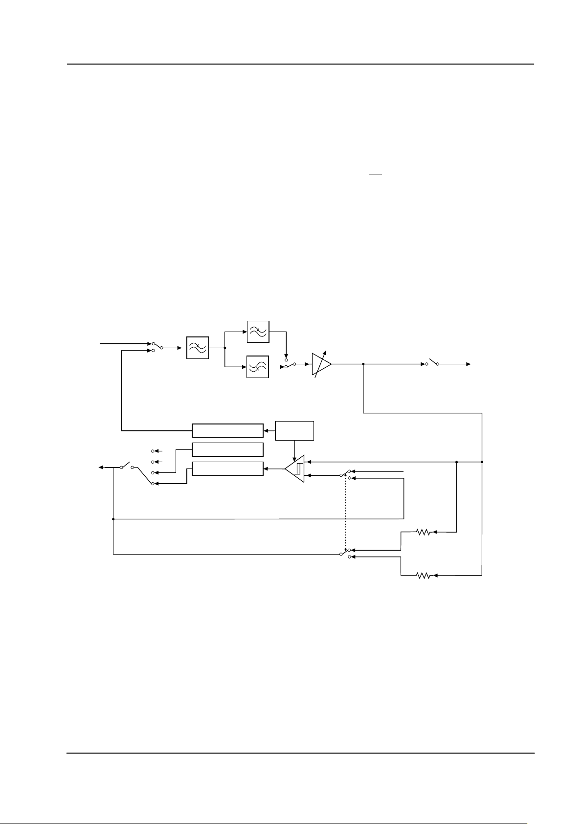
The highly integrated CMX838 Family Radio Processor includes subaudio, audio, and synthesizer functions
to serve as the core engine for low cost, high performance FRS, PMR446, and GMRS radio designs. Its
flexibility supports both simple and advanced multi-channel radios without cost penalties. Integrated Tx
voltage reference and baseband clock generation circuits eliminate the need for external components. The
CMX838’s features directly supports advanced end product functions such as: group calling, scanning,
automatic scanner response tone setup, and Tone Cloning™.
By using the CMX838 one global radio design can support multiple standards and markets.
Controlled via a serial interface (C-BUS) the Family Radio Processor operates from a 3V to 5V supply and is
available in 28-pin TSSOP (CMX838E1) and 28-pin SOIC (CMX838D1) packages.
Page 2

FRS/PMR446/GMRS Family Radio Processor 2 CMX838 Advance Information
¤
¤¤
¤2001 MX-COM, Inc. www.mxcom.com Tel: 800 638 5577 336 744 5050 Fax: 336 744 5054 Doc. # 20480221.002
4800 Bethania Station Road, Winston-Salem, NC 27105-1201 USA All trademarks and service mark s are held by their res pec t ive companies.
CONTENTS
Section Page
1 Block Diagram............................................................................................................... 7
2 Signal List...................................................................................................................... 8
3 External Components................................................................................................. 10
4 General Description....................................................................................................11
4.1 Audio ...............................................................................................................................11
4.1.1 Digitally Controlled Amplifiers (DCA).................................................................................... 11
4.1.2 Transmit Input Amplifier........................................................................................................12
4.1.3 Audio Switched Capacitor Filters.......................................................................................... 12
4.1.3.1 Preemphasis/Low-pass Filter......................................................................................... 13
4.1.3.2 High-pass Filter ..............................................................................................................14
4.1.3.3 Deviation Limiter Low-pass Filter................................................................................... 14
4.1.4 Deemphasis.......................................................................................................................... 15
4.1.5 Transmit Audio Path .............................................................................................................15
4.1.6 Rec ei ve Audio Path ..............................................................................................................16
4.1.7 Aud io Pat h witho ut Deemphasis or Preemphasis ................................................................ 16
4.1.8 Deviation Limiter................................................................................................................... 17
4.2 Tone Signaling Processor................................................................................................18
4.2.1 Tone encoding/decoding ...................................................................................................... 18
4.2.2 Subaudio RX and TX Filter Characteristics.......................................................................... 19
4.2.3 CTCSS Subaudio Decoder and Encoder Tone Set.............................................................. 21
4.2.4 Tone Signaling Processor Configuration Task Descriptions ................................................ 22
4.2.4.1 Normal Run Mode (Task 0)............................................................................................22
4.2.4.2 Reserved For Test (Task 1-3) ........................................................................................ 22
4.2.4.3 RX Configuration ............................................................................................................ 23
4.2.4.4 TX Configuration............................................................................................................. 24
4.2.4.5 Initialize and Configure................................................................................................... 24
4.3 RF Synthesizer ................................................................................................................ 27
4.3.1 Operating Range and Specifications.................................................................................... 27
4.3.2 Main Divider.......................................................................................................................... 27
4.3.3 Phas e Detec t or & Charge Pump .......................................................................................... 27
4.3.4 Lock Detect Output............................................................................................................... 28
4.3.5 Reference Circuits ................................................................................................................ 28
4.4 Baseband Timing Generation ..........................................................................................28
Page 3

FRS/PMR446/GMRS Family Radio Processor 3 CMX838 Advance Information
¤
¤¤
¤2001 MX-COM, Inc. www.mxcom.com Tel: 800 638 5577 336 744 5050 Fax: 336 744 5054 Doc. # 20480221.002
4800 Bethania Station Road, Winston-Salem, NC 27105-1201 USA All trademarks and service mark s are held by their res pec t ive companies.
5 Software Programming............................................................................................... 29
5.1 C-BUS Serial Interface.....................................................................................................29
5.1.1 8-Bit C-BUS Register Map.................................................................................................... 30
5.1.2 16-Bit C-BUS Register Map.................................................................................................. 31
5.1.2.1 GENERAL RESET ($01)................................................................................................31
5.1.2.2 SETUP Register ($80).................................................................................................... 32
5.1.2.3 AUDIO CONTROL Register ($81).................................................................................. 33
5.1.2.4 RX AUDIO LEVEL CONTROL Register ($82) ............................................................... 34
5.1.2.5 AUDIO POWER AND BANDWIDTH CONTROL Register ($83) ................................... 35
5.1.2.6 TXMOD 1 & 2 CONTROL Register ($88)....................................................................... 36
5.1.2.7 SYNTHESIZER BASEBAND CLK CONTROL Register ($89)....................................... 38
5.1.2.8 SYNTHESIZER GENERAL CONTROL Register ($8A)................................................. 39
5.1.2.9 SYNTHESIZER CHANNEL SELECT Register ($8B)..................................................... 40
5.1.2.10 SYNTHESIZER STATUS Register ($8C)....................................................................... 40
5.1.2.11 SYNTHESIZER 1ST IF OFFSET Register ($8D)........................................................... 41
5.1.2.12 16 BIT SUBAUDIO TASK DATA Register ($8E)............................................................ 41
5.1.2.13 16 BIT SUBAUDIO TEST DATA Register ($8F) ............................................................ 41
5.1.2.14 SYNTHESIZER TEST Register ($90) ............................................................................ 41
5.1.2.15 16 BIT SUBAUDIO TEST READ DATA Register ($91) ................................................. 42
5.1.2.16 SUBAUDIO PROCESSOR GENERAL CONTROL Register ($93)................................ 42
5.1.2.17 SUBAUDIO STATUS Register ($94).............................................................................. 43
5.1.2.18 SUBAUDIO TASK 8 BIT DATA Register ($95).............................................................. 43
5.1.2.19 SUBAUDIO ANALOG CONTROL Register ($97).......................................................... 44
6 Application Notes........................................................................................................ 46
6.1 Overview..........................................................................................................................46
6.2 Basic FRS Radio Architecture..........................................................................................47
6.3 CMX838 Architectural Overview ......................................................................................48
6.4 Detailed CMX838 Architecture......................................................................................... 48
6.4.1 Aud io Proc ess ing..................................................................................................................49
6.4.2 Tone Signaling Processor..................................................................................................... 51
6.4.3 Lev el Control......................................................................................................................... 53
6.4.4 Synthesizer and Charge Pump............................................................................................. 55
6.4.5 Clock Generation.................................................................................................................. 55
6.4.6 Powersave Functions ........................................................................................................... 56
6.5 Control Registers Illustrated.............................................................................................56
6.6 Application Examples.......................................................................................................58
6.6.1 CMX 838 Ini tia li za tion ............................................................................................................ 58
6.6.1.1 Register Descriptions: .................................................................................................... 58
6.6.2 TX, subaudio encoding, single point modulation.................................................................. 59
6.6.2.1 Register Descriptions: .................................................................................................... 59
6.6.3 RX, subaudio decode CTCSS tone or tones........................................................................61
6.6.3.1 Register Descriptions: .................................................................................................... 61
6.6.4 RX, multiple subaudio tone detect - Tone Cloning™............................................................ 63
6.6.4.1 Register Descriptions: .................................................................................................... 63
Page 4

FRS/PMR446/GMRS Family Radio Processor 4 CMX838 Advance Information
¤
¤¤
¤2001 MX-COM, Inc. www.mxcom.com Tel: 800 638 5577 336 744 5050 Fax: 336 744 5054 Doc. # 20480221.002
4800 Bethania Station Road, Winston-Salem, NC 27105-1201 USA All trademarks and service mark s are held by their res pec t ive companies.
7 Performance Specification......................................................................................... 65
7.1 Electrical Performance ..................................................................................................... 65
7.1.1 Abs ol ute Maximum Ratings.................................................................................................. 65
7.1.2 Operating Limits....................................................................................................................65
7.1.3 Operating Characteristics ..................................................................................................... 66
7.1.4 Timing................................................................................................................................... 69
7.2 Packaging........................................................................................................................70
MX-COM, Inc. reserves the right to change specifications at any time and without notice.
Page 5

FRS/PMR446/GMRS Family Radio Processor 5 CMX838 Advance Information
¤
¤¤
¤2001 MX-COM, Inc. www.mxcom.com Tel: 800 638 5577 336 744 5050 Fax: 336 744 5054 Doc. # 20480221.002
4800 Bethania Station Road, Winston-Salem, NC 27105-1201 USA All trademarks and service mark s are held by their res pec t ive companies.
FIGURES
Figure Page
Figure 1: Block Diagram.....................................................................................................................................7
Figure 2: Recommended External Components..............................................................................................10
Figure 3: Audio Processing Block Diagram......................................................................................................11
Figure 4: Digitally controlled amplifiers and switch matrix for adjusting and switching transmit audio and
subaudio signals. ..............................................................................................................................12
Figure 5: TX Input Amplifier.............................................................................................................................. 12
Figure 6: Magnitude response for input low-pass filter. ................................................................................... 13
Figure 7: Magnitude response for preemphasis filter.......................................................................................13
Figure 8: Magnitude response of high-pass filter.............................................................................................14
Figure 9: Magnitude response of post-deviation limiter low-pass filter. ........................................................... 14
Figure 10: Magnitude response of deemphasis filter.......................................................................................15
Figure 11: Transmit audio path frequency response with preemphasis. ......................................................... 15
Figure 12: Receive audio path frequency response with deemphasis.............................................................16
Figure 13: Audio path frequency response without preemphasis or deemphasis. .......................................... 16
Figure 14: Deviation limiter block diagram . ......................................................................................................17
Figure 15: Subaudio Block Diagram.................................................................................................................18
Figure 16: Subaudio RX filter gain for normal CTCSS operation.....................................................................19
Figure 17: Subaudio RX filter delay for normal CTCSS operation................................................................... 19
Figure 18: Subaudio TX level for normal CTCSS operation (Magnitude scale with respect to 0dBV) ............20
Figure 19: Subaudio TX filter delay for normal CTCSS operation. ..................................................................20
Figure 20: RF Synthesizer block diagram........................................................................................................27
Figure 21: Block diagram of main programmable divider.................................................................................27
Figure 22: C-BUS transaction timing diagram..................................................................................................29
Figure 23: Basic FRS Radio Tx Architecture ................................................................................................... 47
Figure 24: Basic FRS Radio Rx Architecture...................................................................................................47
Figure 25: CMX838 Main Function Blocks....................................................................................................... 48
Figure 26: CMX838 Main Sections................................................................................................................... 48
Figure 27: Audio Processing ............................................................................................................................ 49
Figure 28: Example Audio RX Path.................................................................................................................. 49
Figure 29: Example Audio TX Voice Path........................................................................................................50
Figure 30: Example Audio TX Internally Generated T one with Lou ds peak er Enabled Path ...........................50
Figure 31: Tone Signaling Processor...............................................................................................................51
Figure 32: Example CTCSS Tone Decoder Path.............................................................................................52
Figure 33: Example CTCSS Tone Encoder Path.............................................................................................52
Figure 34: Example Internal Audio Tone Enco der Pat h................................................................................... 53
Figure 35: Level Control...................................................................................................................................53
Figure 36: Example Single Point Modulati on Level Pat h ................................................................................. 54
Figure 37: Example Two-Point Modulation Level Paths .................................................................................. 54
Figure 38: Example Single Point Modul ation with Varied Subaudio Level Paths............................................54
Figure 39: Synthesizer and Charge Pump.......................................................................................................55
Figure 40: Clock Generation ............................................................................................................................ 55
Figure 41: Powersave Scope and Related Control Regis ters.......................................................................... 56
Page 6

FRS/PMR446/GMRS Family Radio Processor 6 CMX838 Advance Information
¤
¤¤
¤2001 MX-COM, Inc. www.mxcom.com Tel: 800 638 5577 336 744 5050 Fax: 336 744 5054 Doc. # 20480221.002
4800 Bethania Station Road, Winston-Salem, NC 27105-1201 USA All trademarks and service mark s are held by their res pec t ive companies.
Figure 42: Synthesizer to Baseband Clock Control, $89 ................................................................................. 56
Figure 43: Setup, $80.......................................................................................................................................57
Figure 44: Audio ($81), RX Audio Level ($82) and Subaudio Analog ($97) Control ....................................... 57
Figure 45: Audio Power and Bandwidth Control, $83 ...................................................................................... 58
Figure 46: TXMOD1 & TXMOD2 Control, $88.................................................................................................58
Figure 47: Application Exam ple TX, Subaudio Enc od i ng, Sin gle Poi nt Modu lat ion ........................................61
Figure 48: C-BUS Timing ................................................................................................................................. 69
Figure 49: 28-pin TSSOP (E1) Mechanical Outline: Order as part no. CMX838E1 ....................................... 70
Figure 50: 28-pin SOIC (D1) Mechanical Outline: Order as part no. CMX838D1...........................................70
Page 7
FRS/PMR446/GMRS Family Radio Processor 7 CMX838 Advance Information
¤
¤¤
¤2001 MX-COM, Inc. www.mxcom.com Tel: 800 638 5577 336 744 5050 Fax: 336 744 5054 Doc. # 20480221.002
4800 Bethania Station Road, Winston-Salem, NC 27105-1201 USA All trademarks and service mark s are held by their res pec t ive companies.
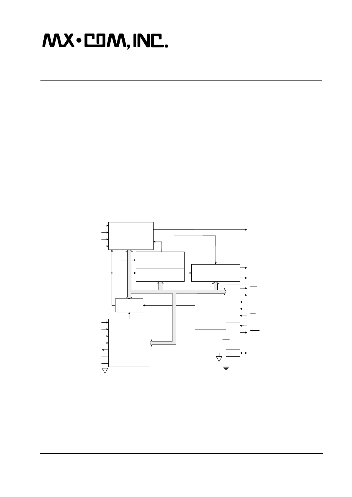
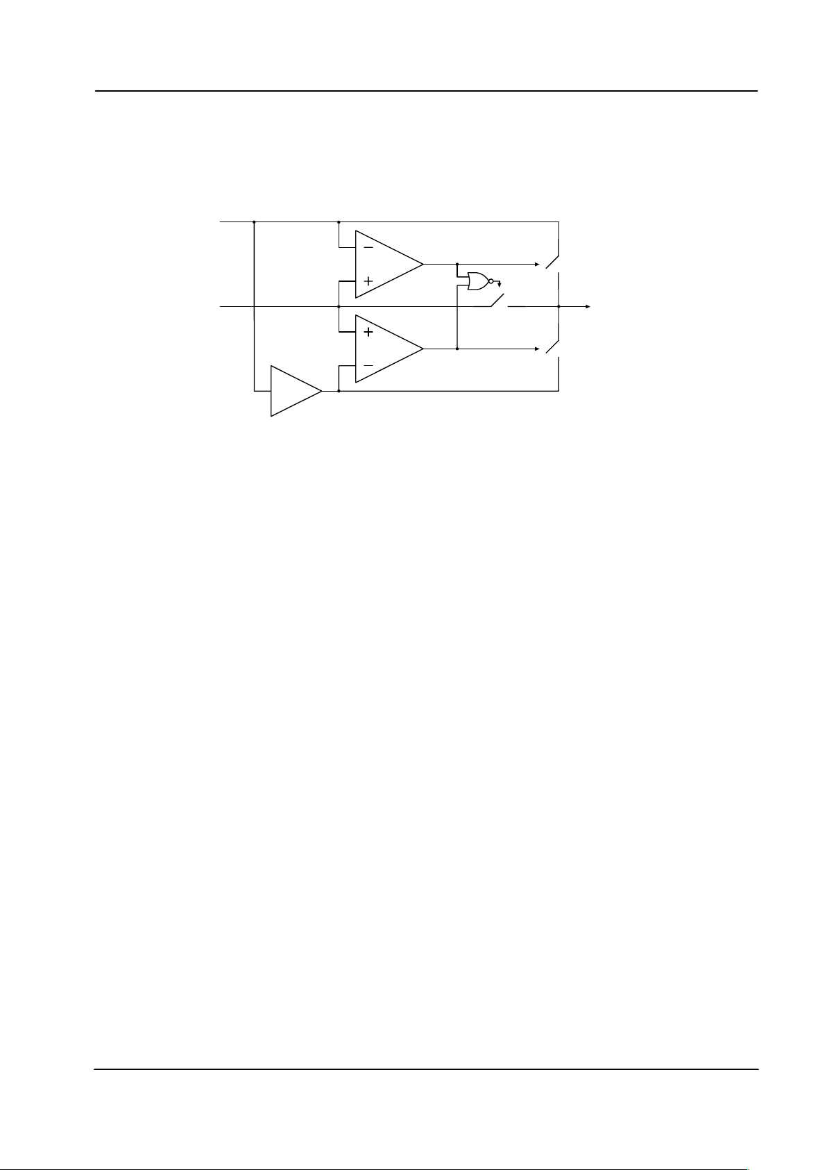
1 Block Diagram
CTCSS DECODERS
+
CTCSS ENCODE
RXIN
BIAS
AUX I/O
C-BUS
Serial
Interface
DIVIDE 32/33
PROGRAMMABLE DIVIDER
12 BIT PROGRAMMABLE
REFERENCE COUNTER
PHASE
DETECTOR
CHARGE
PUMP
LOCK
DETECT
+RF
I N
-RF
I N
REF
I N
SV
SS
SV
DD
V
BIAS
XTAL
XTAL
I
SET
CP
OUT
V
SS
V
DD
S
BASEBAND
TIMING GENERATION
SERIAL CLOCK
CS
LPF
V
BIAS
V
BIAS
V
BIAS
AUDIOTONE ENCODE
0°/180°
phase
0°/180°
phase
CMD DATA
RPLY DATA
IRQ
TXMOD1
TXMOD2
RX NOTONE/
TX DURATION TIMER
VOLTAGE REF
BPF
MICIN
MICOUT
PRE
LPF
HPF
LPF
LIM
B
IN
A
IN
A
OUTBOUT
V
BIAS
VOLTAGE REF
DEEMP
VOLTAGE REF
1
0
V
BIAS
RXOUT
Figure 1: Block Diagram
Page 8

FRS/PMR446/GMRS Family Radio Processor 8 CMX838 Advance Information
¤
¤¤
¤2001 MX-COM, Inc. www.mxcom.com Tel: 800 638 5577 336 744 5050 Fax: 336 744 5054 Doc. # 20480221.002
4800 Bethania Station Road, Winston-Salem, NC 27105-1201 USA All trademarks and service mark s are held by their res pec t ive companies.
2 Signal List
Package Signal Description
Pin No.
E1/D1
Name Type
1 RXIN input Receive input for both audio and subaudio signals.
2 AUX I/O input/output When configured as an input this pin can be used to route
externally generated ringing or alert signals to the Rx and
Tx audio paths.
When configured as an output this pin allows for
monitoring internally generated ringing or alert signals.
See Section 4.2.4.5.3
3 MICOUT output Microphone amplifier feedback output.
4 MICIN input Microphone amplifier input. This is the inverting input to a
high gain opamp, suitable for use with common
microphones.
5 CP
OUT
output Synthesizer charge pump output. Apply to external loop
filter that drives the control input of an external VCO
6
I
SET
input Synthesizer charge pump current control. Connect via
external resistor to SV
SS
to set charge pump current.
7 SVDD power Synthesizer positive supply. This signal must be
decoupled to SV
SS
by a capacitor mounted close to the
device pins.
8 -RFIN input Synthesizer RF negative input. Connect this pin to SVSS
(synthesizer common) when a non-differential input signal
is applied to +RF
IN
.
9 +RFIN input Synthesizer RF positive input.
10 SVSS power Synthesizer negative supply.
11 REFIN input Synthesizer reference oscillator input.
12 XTAL input The input to the on-chip oscillator, for external Xtal circuit
or clock. This input should be connected to V
SS
, Circuit
Common, when the device is configured to generate the
XTAL clock internally from the REF
IN
clock.
13
XTAL
output Inverted output of the on-chip crystal oscillator. This pin
should not be connected (left open) when the device is
configured to generate the XTAL clock internally from the
REF
IN
clock.
14
CS
input C-BUS select data loading control function input. This
input controls C-BUS transfer initiation, completion and
cancellation.
15
IRQ
output Interrupt output, logic '0' active level. This is a 'wire-
Orable' output, enabling the connection of multiple
peripherals to 1 interrupt port on an external µController.
This pin has a low impedance pull-down to logic "0" when
active and a high-impedance when inactive. An external
pull-up resistor is required. Interrupt outputs may be
configured via mask bits via C-BUS commands.
16 RPLY DATA output Reply data output to C-BUS serial control port. Output
reply data bytes are synchronized to the CLK clock input
under the control of the
CS input. This 3-state output is
held at high impedance when not driving output data.
17 CMD DATA input Command data input to C-BUS serial control port. Data is
loaded into this device in 8-bit bytes, MSB (D7) first, and
LSB (D0) last, synchronized to the CLK clock input.
Page 9

FRS/PMR446/GMRS Family Radio Processor 9 CMX838 Advance Information
¤
¤¤
¤2001 MX-COM, Inc. www.mxcom.com Tel: 800 638 5577 336 744 5050 Fax: 336 744 5054 Doc. # 20480221.002
4800 Bethania Station Road, Winston-Salem, NC 27105-1201 USA All trademarks and service mark s are held by their res pec t ive companies.
Package Signal Description
18 SERIAL CLOCK input Serial clock input to C-BUS serial control port. This clock
input controls transfer timing of commands and data to
and from the device.
19 VSS power Negative supply (Circuit Common)
20 TXMOD2 output Transmit Output 2 internally switch selected to be at any
of (1) V
BIAS
, (2) transmit subaudio or (3) transmit audio
summed with subaudio.
21 TXMOD1 output Transmit Output 1 internally switch selected to be at any
of (1) V
BIAS
, (2) transmit audio or (3) transmit audio
summed with subaudio.
22 VDD supply Positive supply. Levels and voltages are dependent upon
this supply. This signal must be decoupled to V
SS
by a
capacitor mounted close to the device pins.
23 RXOUT output Processed receive audio output.
24 BIN input External processing Path B input.
25 AIN input External processing Path A input.
26 V
BIAS
bi-directional A bias line for the internal circuitry, driven to VDD/2 by a
high impedance source. This signal must be decoupled by
a capacitor mounted close to the device pins.
27 B
OUT
output External processing Path B output. This provides internal
switch controlled access to either Rx or Tx audio signals
for external processing such as expanding and
unscrambling.
28 A
OUT
output External processing Path A output. This provides internal
switch controlled access to either Rx or Tx audio signals
for external processing such as compressing and
scrambling.
Table 1: Signal List
Page 10
FRS/PMR446/GMRS Family Radio Processor 10 CMX838 Advance Information
¤
¤¤
¤2001 MX-COM, Inc. www.mxcom.com Tel: 800 638 5577 336 744 5050 Fax: 336 744 5054 Doc. # 20480221.002
4800 Bethania Station Road, Winston-Salem, NC 27105-1201 USA All trademarks and service mark s are held by their res pec t ive companies.
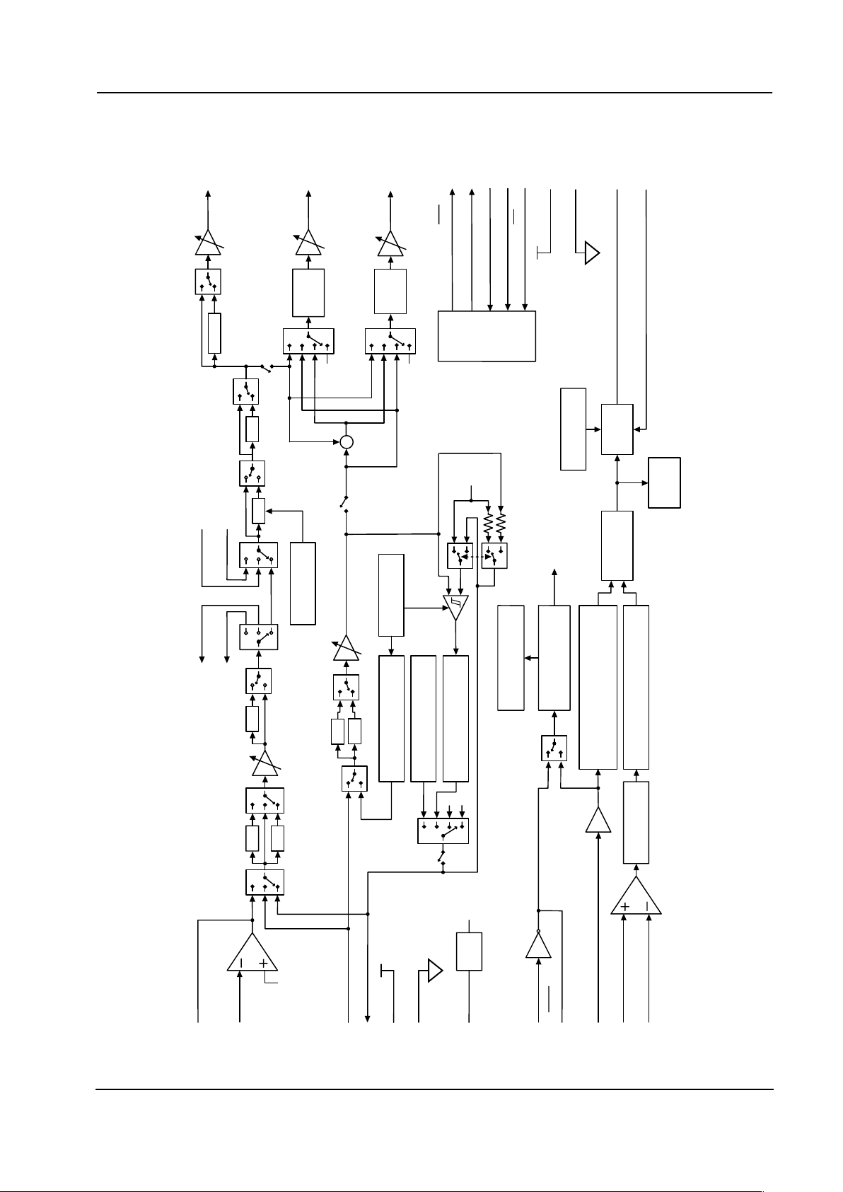
3 External Components
A
OUT
B
OUT
V
BIAS
A
IN
B
IN
RXOUT
V
DD
TXMOD1
TXMOD2
RXIN
IRQ
RPLY DATA
CMD DATA
SERIAL CLOCK
V
SS
CMX838E1
AUX I/O
MICOUT
MICIN
CP
OUT
I
SET
SV
DD
REF
IN
-RF
IN
+RF
IN
SV
SS
XTAL
XTAL
CS
C-BUS
Serial
Control
Interface
C1
C2
C3
C4
C5
C6
C7
C8
C15
C14
C13
C12
C11
C10
C9
U2
RF
Section
REF
OSC
VCO
From RF Receiver
FromTone Generator
Microphone
RF
Section
R1
R2
R4
R3
1
2
3
4
5
6
7
8
9
10
11
12
13
14
28
27
26
25
24
23
22
21
20
19
18
17
16
15
C16
Optional
External
Audio
Processing
Figure 2: Recommended External Components
R1 Note 1
470k
Ω
±5% C9 0.1µF ±20%
R2 Note 1
10k
Ω
±5% C10 0.1µF ±20%
R3 Note 2
100k
Ω
±10% C11 0.1µF ±20%
R4 Note 3 ±10% C12 0.1µF ±20%
C1 0.1µF ±20% C13 0.1µF ±20%
C2 0.1µF ±20% C14 0.1µF ±20%
C3 Note 1 33pF ±20% C15 0.1µF ±20%
C4 Note 1 0.1µF ±20% C16 47.0pF ±20%
C5 Note 2 0.1µF ±20%
C6 0.1µF ±20%
C7 0.1µF ±20% U2 Speaker driver
e.g. LM386
C8 0.1µF ±20%
External Components Notes:
1. R1, R2, C3 and C4 form the gain components for the Tx Input Amplifier (microphone amplifier). R1
should be chosen as required by the signal level, using the following formula:
Gain = -R1/R2
C3 x R1 should be chosen so as not to compromise the high frequency performance and C4 x R2
should be chosen so as not to compromise the low frequency performance.
2. R3 and C5 values are dependent on microphone specifications.
3. R4 Sets charge pump source current. The value of R4 can vary between about 50k
Ω and 250kΩ. This
gives a charge pump current range of 0.8mA to 8.4mA
Page 11
FRS/PMR446/GMRS Family Radio Processor 11 CMX838 Advance Information
¤
¤¤
¤2001 MX-COM, Inc. www.mxcom.com Tel: 800 638 5577 336 744 5050 Fax: 336 744 5054 Doc. # 20480221.002
4800 Bethania Station Road, Winston-Salem, NC 27105-1201 USA All trademarks and service mark s are held by their res pec t ive companies.
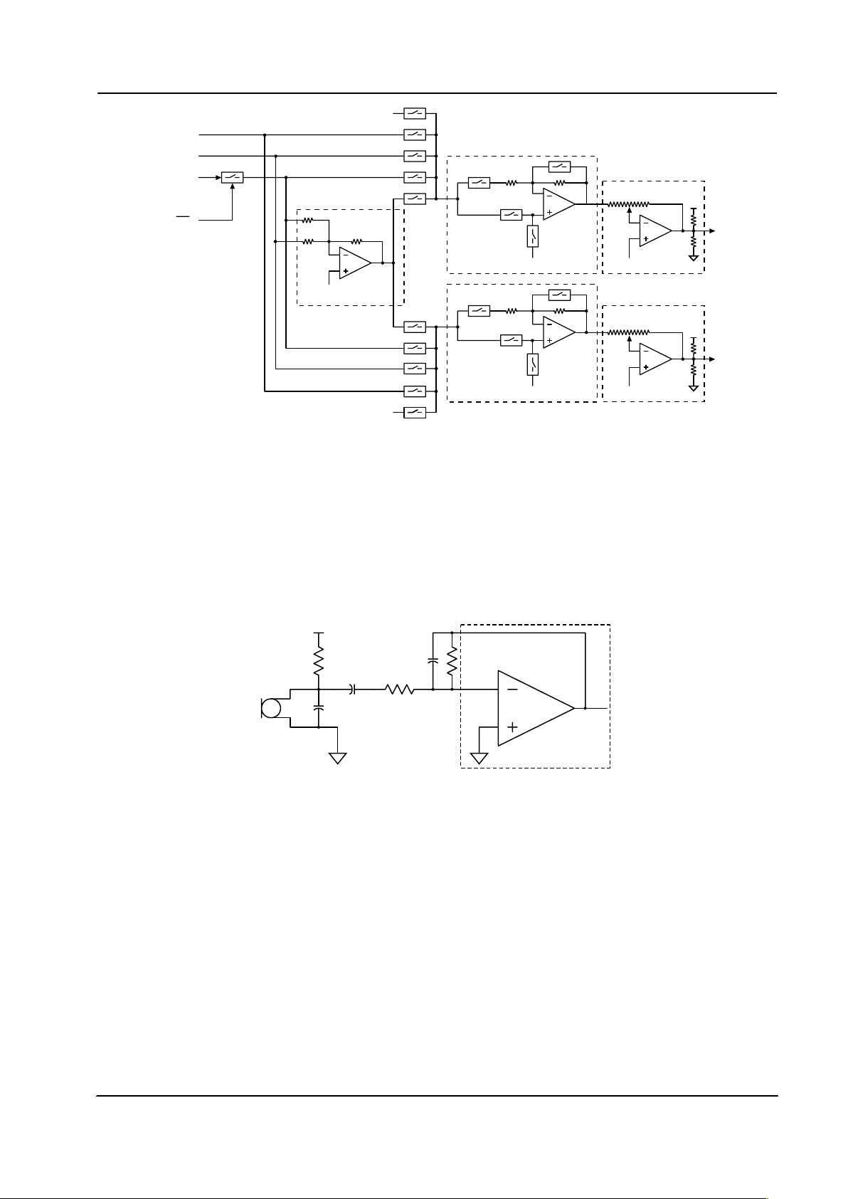
4 General Description
4.1 Audio
The audio signal processing is designed to meet or exceed the requirements for basic audio filtering, gain
control and deviation limiting in a FRS radio. Figure 3 is a block diagram of the audio circuitry.
RXIN
TX SUBAUDIO (From On-Chip SubaudioTone Generator)
RXOUT
AUX I/O
MICIN
MICOUT
V
REF
LP
PRE
1
1
1
DE
1
TXMOD1
A
OUT
B
OUT
A
IN
B
IN
DEEMPHASIS NETWORK
DEVIATION LIMITER AND POST-LIMITER LPF
PREEMPHASIS OR 2
ORDER LPF
ND
6 ORDER HPF
TH
LPF BYPASS
LIMITER BYPASS
AUDIO
INPUT 1
SELECT
AUDIO OUT
SELECT
PRE LPF CTRL HPF BYPASS
DEBP
RX AUDIO OUT
LEVEL
AUDIO
LEVEL
V
REF
V
BIAS
TOS
VLHVLL
TOS
TXMOD2
TX/RX
TONE GENERATOR
AUXPUPEN
AUDIO
INPUT 2
SELECT
TXMOD
SWITCH
MATRIX and
PHASE
CONTROL
See Figure 4
Figure 3: Audio Processing Block Diagram
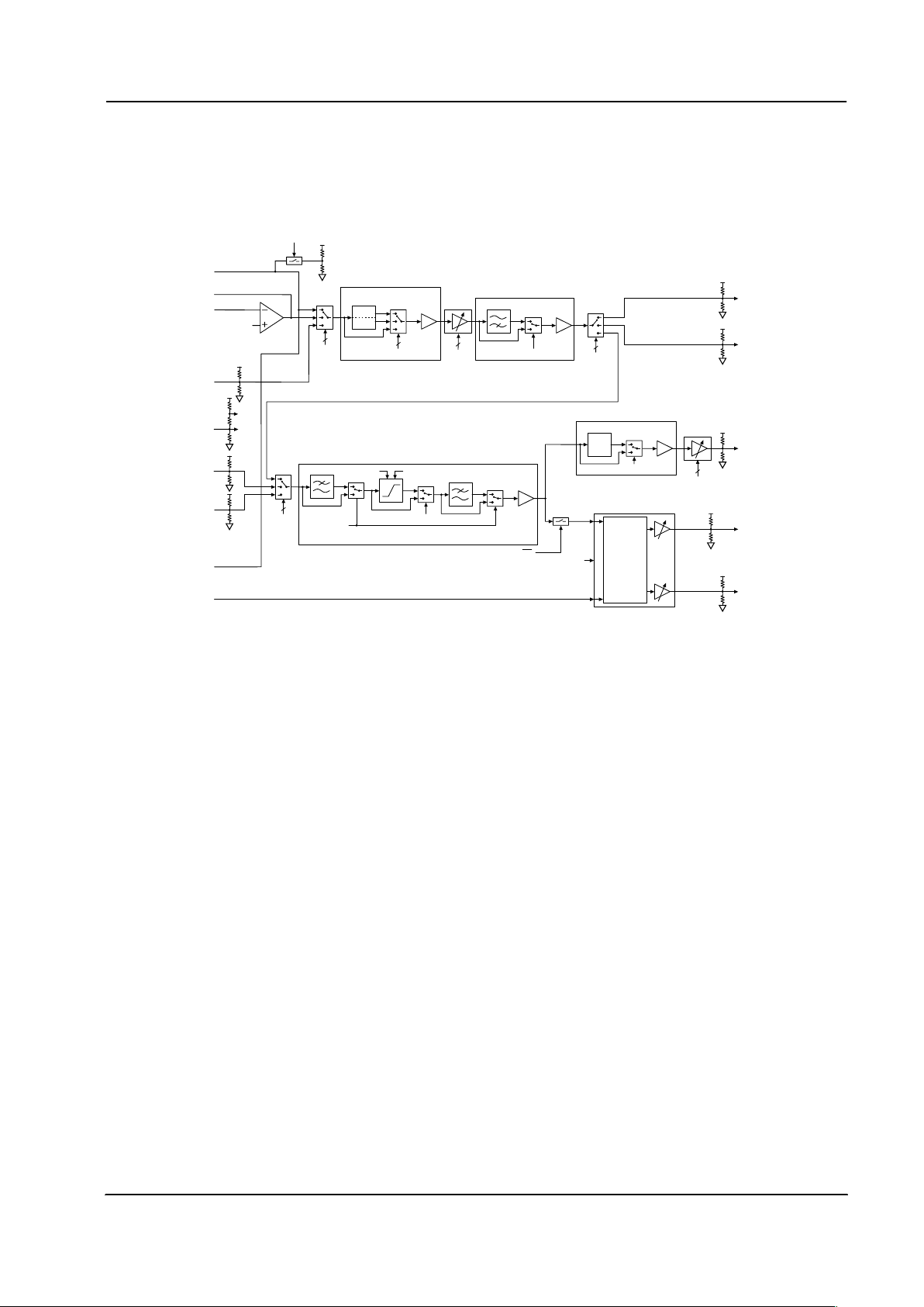
4.1.1 Digitally Controlled Amplifiers (DCA )
There are five DCAs on-chip. They are used to set signal levels for audio in/out, subaudio in/out, receive
audio out (volume control), modulation out1, and modulation out2. The audio in/out DCA is adjustable in
0.5dB steps over a +7.5dB to –7.5dB range, see Section 5.1.2.3.
The volume control level DCA is adjustable
in 1.5dB steps over a +12dB to –33dB range, see Section 5.1.2.4. The subaudio signal level in/out DCA is
adjustable in 0.5dB steps over a +7.5dB to –7.5dB range, see Section 5.1.2.19
The modulation level controls are composed of two DCAs, and a switch matrix, see Figure 4. Each
modulation level DCA, modulation out1 and modulation out2, can be switched to select either the output of
the audio processor, or the output of the tone generator, or the addition of the audio and tone. In addition,
there is an internally generated DC volume (labeled ‘TOS’ in Figure 4), which can be sent to the MOD1 and
MOD2 DCA’s. This signal is not generally applicable to FRS radios. However, in some cases it may be
desirable for testing or signal generation. The modulation out1 DCA is adjustable in 0.5dB steps over a
+7.5dB to –7.5dB range and the Modulation Out2 DCA is adjustable in 0.25dB steps over a +3.75dB to
-3.75dB range, see Section 5.1.2.6. To obtain inverse signals of mod 1and mod 2, the MSB from the first byte
(bit 7) and the MSB from second byte (bit 15) have to set to logic 1, see Section 5.1.2.6.
Page 12
FRS/PMR446/GMRS Family Radio Processor 12 CMX838 Advance Information
¤
¤¤
¤2001 MX-COM, Inc. www.mxcom.com Tel: 800 638 5577 336 744 5050 Fax: 336 744 5054 Doc. # 20480221.002
4800 Bethania Station Road, Winston-Salem, NC 27105-1201 USA All trademarks and service mark s are held by their res pec t ive companies.
TXMOD1
TXMOD2
V
BIAS
V
BIAS
V
BIAS
V
BIAS
V
BIAS
V
BIAS
TOS
SUBAUDIOTONE IN
LOW R
LOW R
LOW R
LOW R
LOW R
LOW R
LOW R
LOW R
SUM
Gain/Attenuation
Gain = +/-1
TX/RX
V
BIAS
Gain/Attenuation
Gain = +/-1
AUDIO IN
Figure 4: Digitally controlled amplifiers and switch matrix for adjusting and switching transmit audio
and subaudio signals.
4.1.2 Transmit Input Amplifier
The transmit input amplifier is a high gain low-noise operational amplifier. Figure 5 is a simplified schematic
showing the external components required for typical application with an electret condenser microphone. The
external component values should be selected such that the feedback resistor will be greater than 10k
Ω and
the minimum gain should be greater than 6dB.
In some cases, it may be desirable to implement a pre-emphasis characteristic of appropriately configuring
the external component values around the TX input amplifier. In this case, the internal preemphasis should be
bypassed (via C-BUS).
Figure 5: TX Input Amplifier
4.1.3 Audio Switched Capacitor Filters
Four standard (composed of biquadratic sections) switched capacitor filters are used in the audio section. A
preemphasis filter (+6dB per octave from 300 to 3000 Hz intended for transmit only) is implemented using
2
nd
order switched capacitor network, which can be configured (via C-BUS) to be a 2nd order low-pass. A
6
th
order high-pass filter is used to remove subaudible tones and bandwidth limit the incoming receive or
transmit audio signal prior to being input to the limiter. A 4
th
order low-pass filter follows the deviation limiter.
This filter smoothes the transients generated by the deviation limiter. Finally, a deemphasis filter (-6dB per
octave from 300 to 3000 Hz intended for receive only) is implemented using a 2
nd
order switched capacitor
network. See Section 5.1.2 for details on configuring audio filters.
Page 13
FRS/PMR446/GMRS Family Radio Processor 13 CMX838 Advance Information
¤
¤¤
¤2001 MX-COM, Inc. www.mxcom.com Tel: 800 638 5577 336 744 5050 Fax: 336 744 5054 Doc. # 20480221.002
4800 Bethania Station Road, Winston-Salem, NC 27105-1201 USA All trademarks and service mark s are held by their res pec t ive companies.
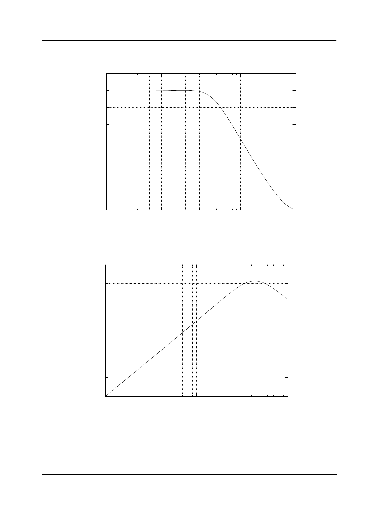
4.1.3.1 Preemphasis/Low-pass Filter
Figure 6 shows magnitude response for the Input Preemphasis/Low-pass Filter when programmed for lowpass mode. This mode would typically be selected when processing Rx audio.
-35
-30
-25
-20
-15
-10
-5
0
5
1000 10000
Magnitude (dB)
Frequency (Hz)
Figure 6: Magnitude response for input low-pass filter.
Figure 7 shows magnitude response for the Input Preemphasis/Low-pass Filter when programmed for
Preemphasis mode. This mode would typically be selected when processing Tx audio.
-20
-15
-10
-5
0
5
10
15
100 1000 10000
Magnitude (dB)
Frequency (Hz)
Figure 7: Magnitude response for preemphasis filter.
Page 14
FRS/PMR446/GMRS Family Radio Processor 14 CMX838 Advance Information
¤
¤¤
¤2001 MX-COM, Inc. www.mxcom.com Tel: 800 638 5577 336 744 5050 Fax: 336 744 5054 Doc. # 20480221.002
4800 Bethania Station Road, Winston-Salem, NC 27105-1201 USA All trademarks and service mark s are held by their res pec t ive companies.
4.1.3.2 High-pass Filter
Figure 8 shows the magnitude response for the Audio High Pass Filter. This filter’s purpose is to suppress
subaudio tones when processing both Rx and Tx audio.
-80
-70
-60
-50
-40
-30
-20
-10
0
10
10 100 1000 10000
Magnitude (dB)
Frequency (Hz)
Figure 8: Magnitude response of high-pass filter.
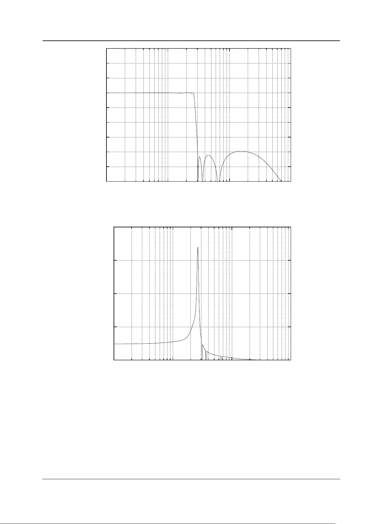
4.1.3.3 Deviation Limiter Low-pass Filter
The magnitude response for narrowband and wideband modes is shown in Figure 9. Narrow-band mode is
generally required for transmitting in systems having RF Channel BW
≤12.5kHz (e.g. FRS).
-40
-35
-30
-25
-20
-15
-10
-5
0
5
1000 10000
Magnitude (dB)
Frequency (Hz)
WIDE BAND
NARROW BAND
Figure 9: Magnitude response of post-deviation limiter low-pass filter.
Page 15
FRS/PMR446/GMRS Family Radio Processor 15 CMX838 Advance Information
¤
¤¤
¤2001 MX-COM, Inc. www.mxcom.com Tel: 800 638 5577 336 744 5050 Fax: 336 744 5054 Doc. # 20480221.002
4800 Bethania Station Road, Winston-Salem, NC 27105-1201 USA All trademarks and service mark s are held by their res pec t ive companies.
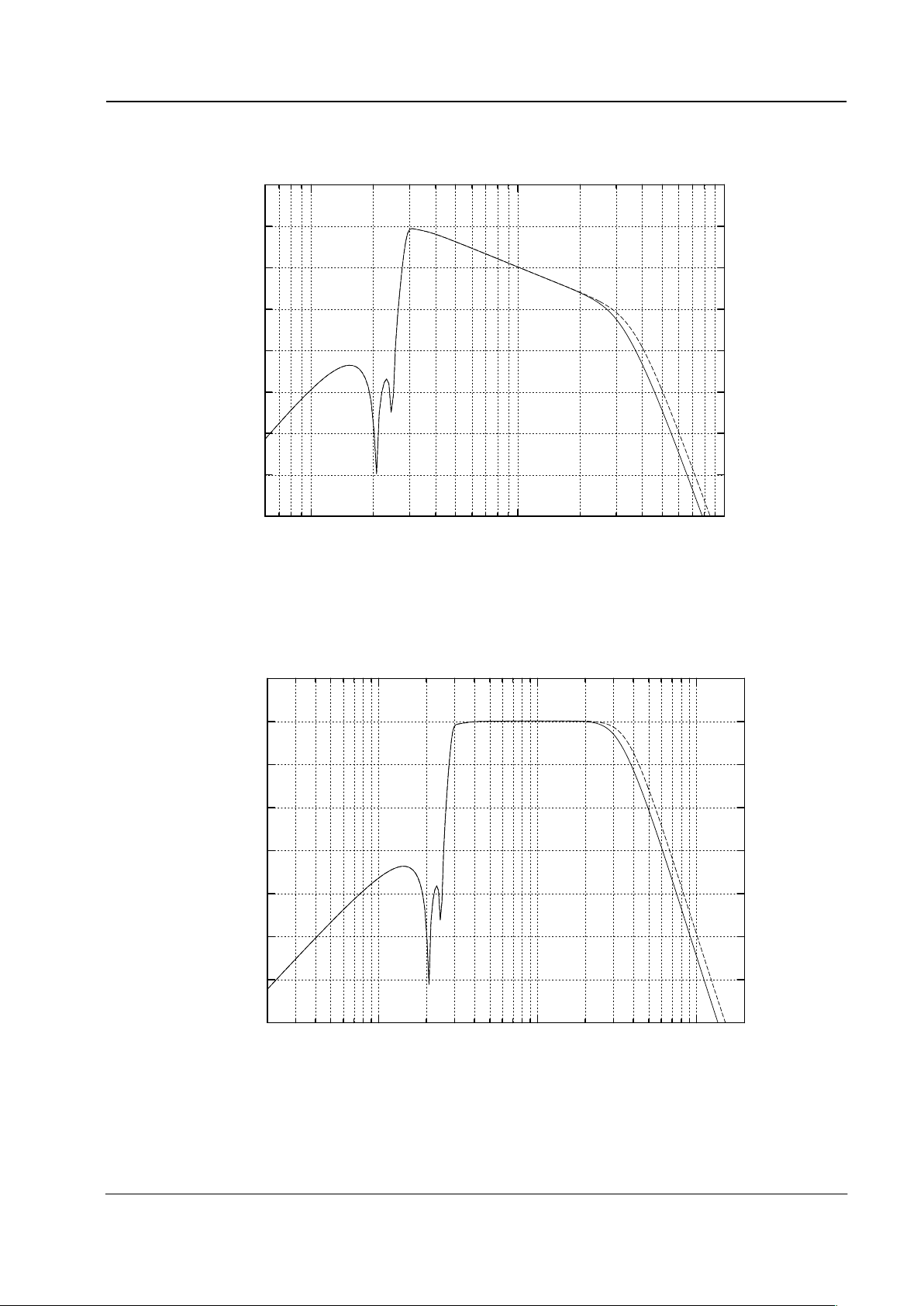
4.1.4 Deemphasis
Figure 10 shows magnitude response for the Deemphasis Filter. This filter precedes the Rx Audio Level
Control and is generally required to process Rx audio.
-20
-15
-10
-5
0
5
10
15
100 1000 10000
Magnitude (dB)
Frequency (Hz)
Figure 10: Magnitude response of deemphasis filter.
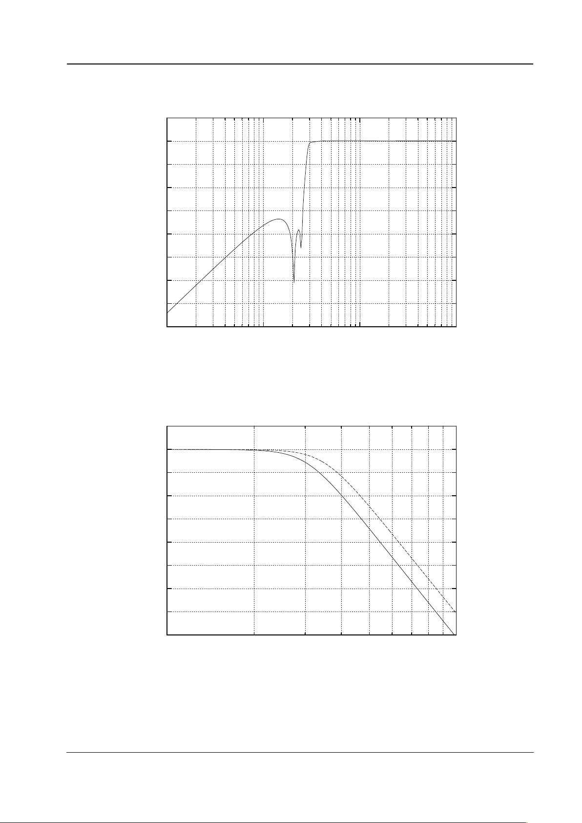
4.1.5 Transmit Audio Path
Overall magnitude response for the transmit audio path for wideband and narrowband with preemphasis is
shown in Figure 11.
-80
-60
-40
-20
0
20
100 1000 10000
Magnitude (dB)
Frequency (Hz)
NARROW BAND
WIDE BAND
Figure 11: Transmit audio path frequency response with preemphasis.
Page 16
FRS/PMR446/GMRS Family Radio Processor 16 CMX838 Advance Information
¤
¤¤
¤2001 MX-COM, Inc. www.mxcom.com Tel: 800 638 5577 336 744 5050 Fax: 336 744 5054 Doc. # 20480221.002
4800 Bethania Station Road, Winston-Salem, NC 27105-1201 USA All trademarks and service mark s are held by their res pec t ive companies.
4.1.6 Receive Audio Path
Overall magnitude response for the receive audio path for wideband and narrowband with deemphasis is
shown in Figure 12.
-60
-50
-40
-30
-20
-10
0
10
20
100 1000 10000
Magnitude (dB)
Frequency (Hz)
NARROW BAND
WIDE BAND
Figure 12: Receive audio path frequency response with deemphasis.
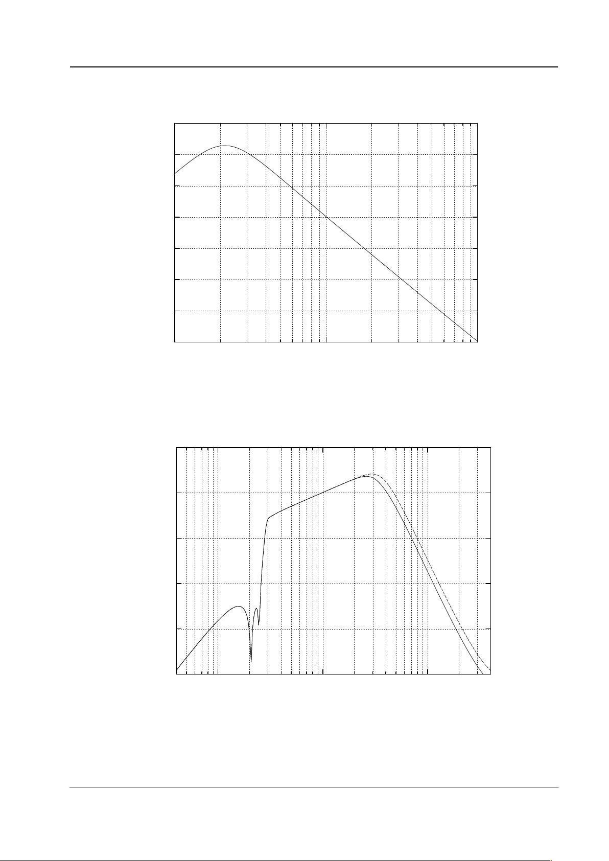
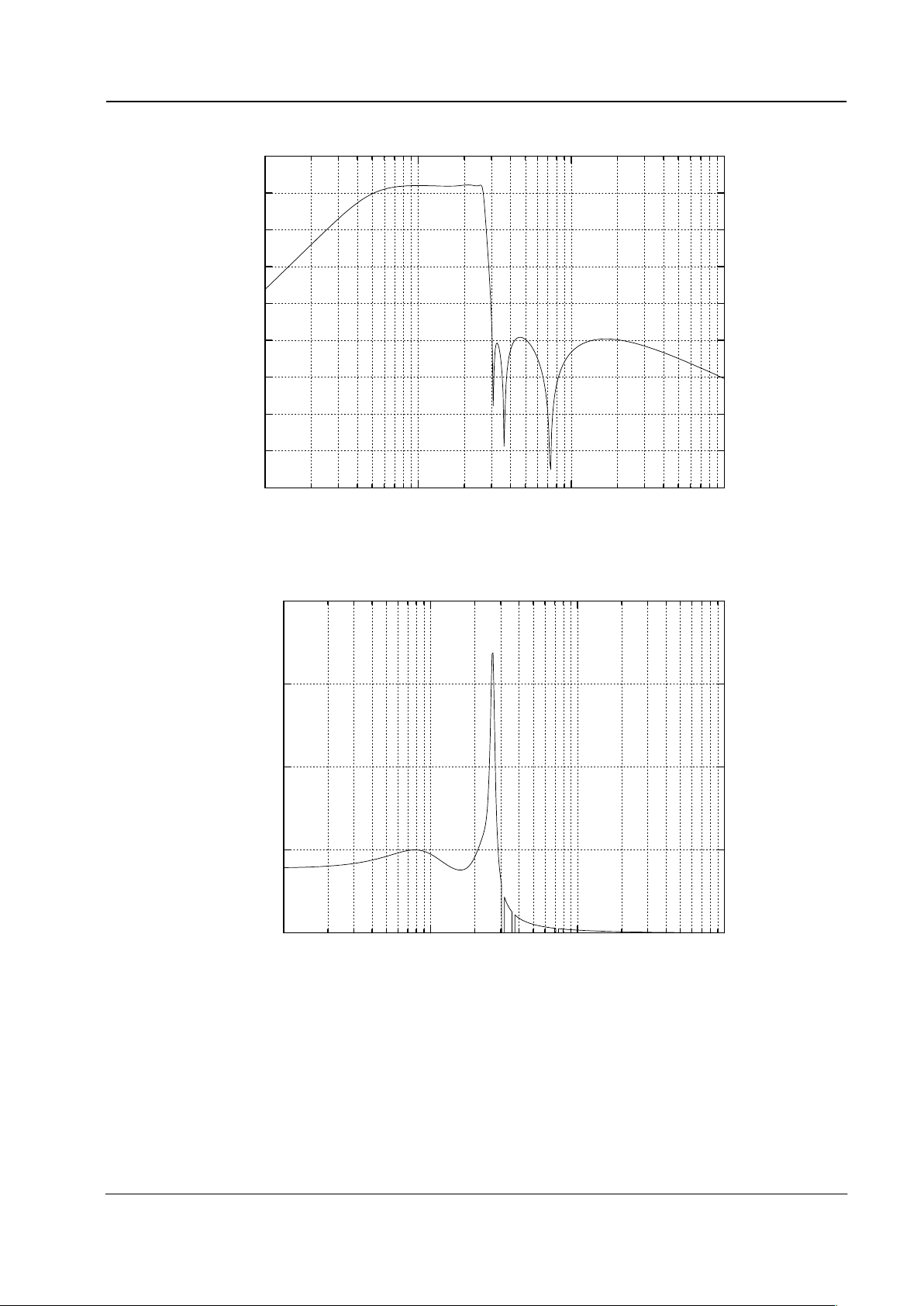
4.1.7 Audio Path without Deemphasis or Preemphasis
The magnitude response for the audio path (could apply to transmit or receive) without the preemphasis or
deemphasis is shown in Figure 13.
-70
-60
-50
-40
-30
-20
-10
0
10
100 1000 10000
Magnitude (dB)
Frequency (Hz)
NARROW BAND
WIDE BAND
Figure 13: Audio path frequency response without preemphasis or deemphasis.
Page 17
FRS/PMR446/GMRS Family Radio Processor 17 CMX838 Advance Information
¤
¤¤
¤2001 MX-COM, Inc. www.mxcom.com Tel: 800 638 5577 336 744 5050 Fax: 336 744 5054 Doc. # 20480221.002
4800 Bethania Station Road, Winston-Salem, NC 27105-1201 USA All trademarks and service mark s are held by their res pec t ive companies.
4.1.8 Deviation Limiter
The purpose of the deviation limiter is to limit the signal level at baseband prior to reaching the RF modulator.
This is necessary to avoid co-channel interference as well as conform to the spectral constraints stipulated by
regulatory agencies (e.g. FCC). Figure 14 is a block diagram of the limiter circuitry. Applying a DC voltage
between V
DD
and VDD/2 to the reference input sets the maximum peak-to-peak signal level. This reference is
internally set so the maximum signal level is 2.196V
P-P
and is constant over supply voltage.
-1
REF
I N
TX AUDIO
LIMITED SPEECH TO
POST DEVIATION
LIMITER FILTER
Figure 14: Deviation limiter block diagram.
Page 18
FRS/PMR446/GMRS Family Radio Processor 18 CMX838 Advance Information
¤
¤¤
¤2001 MX-COM, Inc. www.mxcom.com Tel: 800 638 5577 336 744 5050 Fax: 336 744 5054 Doc. # 20480221.002
4800 Bethania Station Road, Winston-Salem, NC 27105-1201 USA All trademarks and service mark s are held by their res pec t ive companies.
4.2 Tone Signaling Processor
4.2.1 Tone encoding/decoding
The tone signaling processor includes CTCSS encode and decode functions as well as an audio frequency
ringing/alert tone generator. The signaling processor is comprised of a configurable analog filter controlled by
the SUBAUDIO ANALOG CONTROL Register ($97) and a digital processor controlled by configuration tasks.
All device configuration data is passed over the device’s C-BUS serial interface. The configuration tasks to
setup the digital processor are simply C-BUS transaction sequences, which download task argument data
followed by a task request command. In typical applications, once the tone signaling processor is initialized,
its primary behavior (CTCSS encode and decode) is steered by the
RXTX/ bit of the SETUP Register ($80).
The subaudio filter is shared between transmit and receive. It is used to remove the speech signal from the
receive subaudio signal, leaving only the subaudible squelch signal as input to the digital processor. This filter
is also used to smooth the digitally generated subaudible signals in the transmit mode. Following the filter is a
gain trimmer stage that can adjust the signal level
±7.5dB in 0.5dB steps into the decoding section or out to
the modulation section. Approximately 20dB of gain is provided in the receive path and 20dB of attenuation in
the transmit path.
LPF1
CTCSS encode
CTCSS decoders
Band Gap
Reference
audio tone encode
V
BIAS
0
1
RXIN
to Modulation
Control Block
AUX
AUX Output
Control
Task
External DC
Restoration
Subaudio
Filter
Input
Select
Subaudio
HPF/LPF
Select
Subaudio
Filter
Output
Enable
Subaudio
LPF1
Gain
2 or 22db
HPF
LPF2
Subaudio
RX and TX
Levels
-7.5 to 7.5dB
External DC
Restoration
Control with
Initialization Tasks
Subaudio
LPF2
Gain
0 or -18dB
Figure 15: Subaudio Block Diagram
Page 19
FRS/PMR446/GMRS Family Radio Processor 19 CMX838 Advance Information
¤
¤¤
¤2001 MX-COM, Inc. www.mxcom.com Tel: 800 638 5577 336 744 5050 Fax: 336 744 5054 Doc. # 20480221.002
4800 Bethania Station Road, Winston-Salem, NC 27105-1201 USA All trademarks and service mark s are held by their res pec t ive companies.
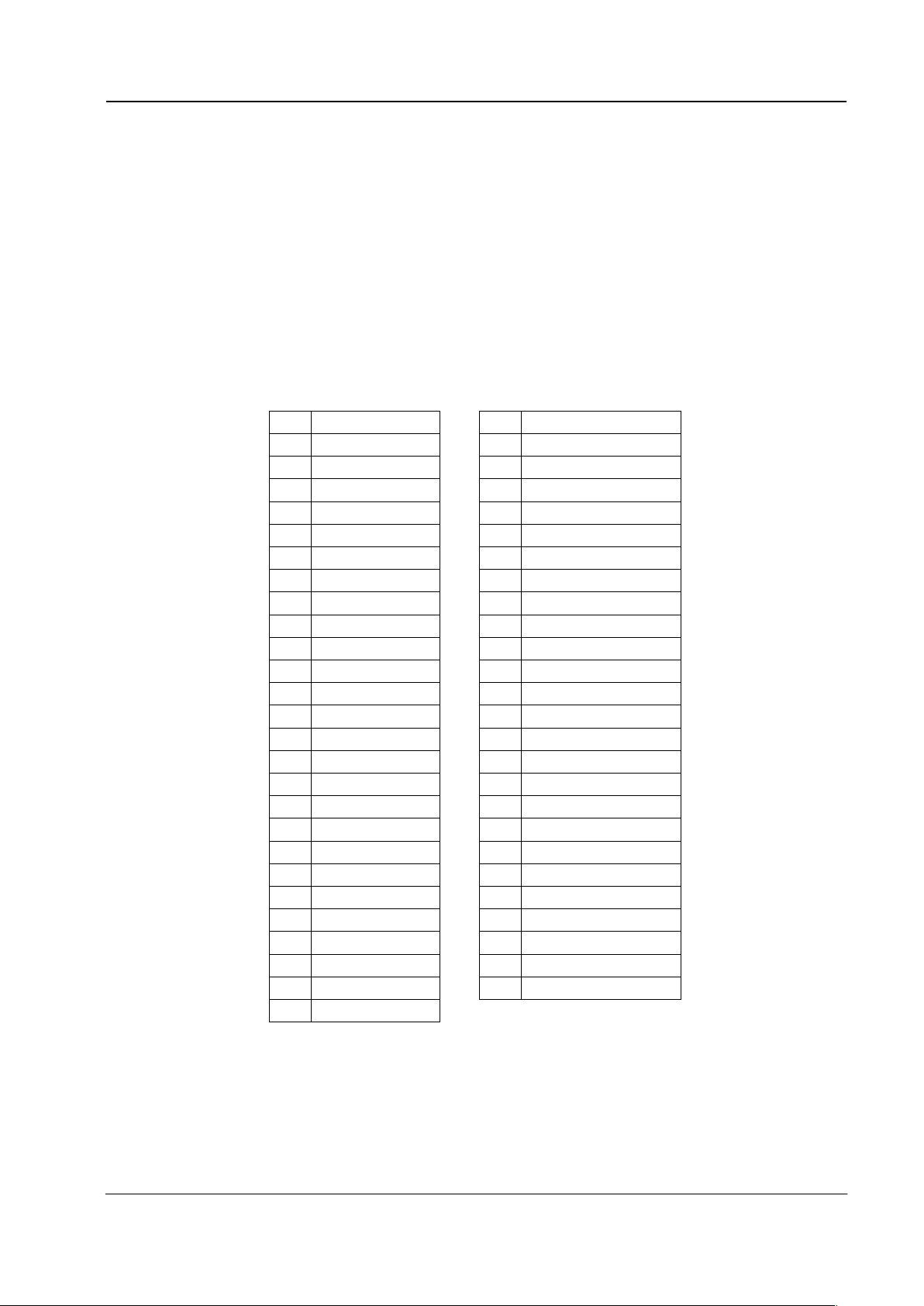
4.2.2 Subaudio RX and TX Filter Characteristics
-60
-50
-40
-30
-20
-10
0
10
20
30
10 100 1000 10000
Magnitude (dB)
Frequency (Hz)
Figure 16: Subaudio RX filter gain for normal CTCSS operation.
0
0.005
0.01
0.015
0.02
10 100 1000 10000
Delay (sec)
Frequency (Hz)
Figure 17: Subaudio RX filter delay for normal CTCSS operation.
Page 20
FRS/PMR446/GMRS Family Radio Processor 20 CMX838 Advance Information
¤
¤¤
¤2001 MX-COM, Inc. www.mxcom.com Tel: 800 638 5577 336 744 5050 Fax: 336 744 5054 Doc. # 20480221.002
4800 Bethania Station Road, Winston-Salem, NC 27105-1201 USA All trademarks and service mark s are held by their res pec t ive companies.
-90
-80
-70
-60
-50
-40
-30
-20
-10
0
10 100 1000 10000
Magnitude (dB)
Frequency (Hz)
Figure 18: Subaudio TX level for normal CTCSS operation (Magnitude scale with respect to 0dBV)
0
0.005
0.01
0.015
0.02
10 100 1000 10000
Delay (sec)
Frequency (Hz)
Figure 19: Subaudio TX filter delay for normal CTCSS operation.
Page 21
FRS/PMR446/GMRS Family Radio Processor 21 CMX838 Advance Information
¤
¤¤
¤2001 MX-COM, Inc. www.mxcom.com Tel: 800 638 5577 336 744 5050 Fax: 336 744 5054 Doc. # 20480221.002
4800 Bethania Station Road, Winston-Salem, NC 27105-1201 USA All trademarks and service mark s are held by their res pec t ive companies.
4.2.3 CTCSS Subaudio Decoder and Encoder Tone Set
The CMX838 supports all popular subaudio tones with a unique, full performance, 'one-of-any' rapid detect
capability that adds support for end product group calling and Tone Cloning™ features. The digital processor
essentially contains 51 decoders to analyze the receive signal. Each decoder can independently be enabled
or disabled via configuration tasks.
The result of the subaudio signal analysis is available in the subaudio status register ($94). Both a decode
status bit, and a decoder index number are reported in the status register. The decode status bit is a logic one
when an enabled decoder senses that the input signal matches its center frequency – the index number will
be that of the matching decoder. If the input signal does not contain a subaudio signal that matches an
enabled decoder’s center frequency then the status bit is a logic zero – in this case the decoder index number
is reported as:
A. 62 if there is a significant subaudio frequency present.
B. 63 if the no tone timer has expired indicating there is no significant subaudio frequency present now, or
C. 0 if no subaudio signal has been seen since the subaudio processor was enabled or most recently placed
in RX mode.
No. Frequency (Hz) No. Frequency (Hz)
1. 67.0 27. 159.8*
2. 69.3 28. 162.2
3. 71.9 29. 165.5*
4. 74.4 30. 167.9
5. 77.0 31. 171.3*
6. 79.7 32. 173.8
7. 82.5 33. 177.3*
8. 85.4 34. 179.9
9. 88.5 35. 183.5*
10. 91.5 36. 186.2
11. 94.8 37. 189.9*
12. 97.4 38. 192.8
13. 100.0 39. 196.6*
14. 103.5 40. 199.5*
15. 107.2 41. 203.5
16. 110.9 42. 206.5*
17. 114.8 43. 210.7
18. 118.8 44. 218.1
19. 123.0 45. 225.7
20. 127.3 46. 229.1*
21. 131.8 47. 233.6
22. 136.5 48. 241.8
23. 141.3 49. 250.3
24. 146.2 50. 254.1*
25. 151.4 51. User Programmable
26. 156.7
* Subaudible Tones not included in TIA-603 standard
Table 2: CTCSS Subaudio Tone Frequencies with their Corresponding Index Number
Page 22

FRS/PMR446/GMRS Family Radio Processor 22 CMX838 Advance Information
¤
¤¤
¤2001 MX-COM, Inc. www.mxcom.com Tel: 800 638 5577 336 744 5050 Fax: 336 744 5054 Doc. # 20480221.002
4800 Bethania Station Road, Winston-Salem, NC 27105-1201 USA All trademarks and service mark s are held by their res pec t ive companies.
4.2.4 Tone Signaling Processor Configuration Task Descriptions
Task ID Task Description Argument Data In
Normal Run Mode 0 Normal Operation N/A
Reserved For Test 1, 2, 3 Special Test Functions N/A
4 Enable/Disable Tone Detector $95
5 Program User Defined Subaudio Tone $8E
6 Adjust Detector Band Width $8E
RX Configure
7 Adjust No Tone Timer Duration $8E
8 Select Sub-Audio Tone From Preprogrammed List $95
9 Program User Defined Subaudio Tone $8E
10 Program Audio Frequency Ringing Tone $8E
TX Configure
11 Program TX Timer $8E
12 Enter Fast Initialization Mode N/A
13 Quickly Enable/Disable Multiple Detectors $95
14 Configure Aux Pin as Output $95
Initialize and Configure
15 Soft Reset N/A
Table 3: Tone Signaling Processor Initialization and Configuration Tasks
Tone signaling configuration tasks initialize the tone signaling processor. While the processor is running,
either generating or detecting tones (controlled by the
RXTX
/
bit of register $80), configuration tasks can be
issued at a rate up to one per 250
µs. The required argument register(s) should not be modified for at least
this time after issuing a task. Before issuing tasks that require argument data, first load the argument data in
the argument data register. Then load the desired task in the task field of the sub-audio general control
register. The Power control (i.e. enabled) and IRQ control (set however you want) should be logically OR’ed
with the desired task field to define the data to load in register $93. All C-BUS writes to the subaudio general
control register ($93), that enable (or keep enabled) the tone signaling processor, constitute issuing a task.
Before tasks are issued, the base band clocks must be setup.
4.2.4.1 Normal Run Mode (Task 0)
To place the device in Normal Run mode issue Task 0. In this mode, the tone signaling processor will either
encode or decode depending on the
RXTX
/
bit of register ($80).
4.2.4.2 Reserved For Test (Task 1-3)
Do not issue tasks 1, 2 or 3 as these are reserved for test.
Page 23

FRS/PMR446/GMRS Family Radio Processor 23 CMX838 Advance Information
¤
¤¤
¤2001 MX-COM, Inc. www.mxcom.com Tel: 800 638 5577 336 744 5050 Fax: 336 744 5054 Doc. # 20480221.002
4800 Bethania Station Road, Winston-Salem, NC 27105-1201 USA All trademarks and service mark s are held by their res pec t ive companies.
4.2.4.3 RX Configuration
The following four tasks are used to control the decode behavior.
4.2.4.3.1 Enable or Disable Tone Detector (Task 4)
This task can be used to enable or disable tone detectors 1 to 51. Tone Detectors 1 to 50 have preset
detection center frequencies while tone detector 51 has a user programmable center frequency. This task
may be issued multiple times to configure a tone watch list. It is recommended not to include non TIA-603
tones with their adjacent TIA tones in a watch list.
Load argument in register $95, then issue task 4. Repeat as needed to configure tone watch list.
The argument data has the following format in the 8 bit task data register ($95).
Bit 7 Bit 6 Bits 5-0
1=enable
0=disable
Don’t
care
Tone detector index number (1-51)
Additionally using index 63 can enable or disable all detectors while issuing just
one task. Enabling index 62 enables detection of all TIA-603 Tones. There is no
single command to disable just the TIA-603 Tone Detectors – instead use index 63
to disable all detectors.
For example to enable the 67Hz Tone Detector:
$95 0x81 // data to enable tone index 1 (67Hz)
$93 0x64 // task command to actually enable tone detector (and IRQ’s)
4.2.4.3.2 Program User Defined RX Sub-Audio Tone (Task 5)
This task is used to program the center frequency of user programmable detector 51. Load the Argument
value in register $8E, then issue task 5.
The argument can be calculated according to the following equations.
RNArgument
f
N
INTR
f
INTN
+⋅=
¸
¸
¹
·
¨
¨
©
§
⋅
⋅
−+=
¸
¹
·
¨
©
§
⋅⋅
=
64
96
100000
5115.0
100000
51196
The argument data for 65 Hz would be 31*64+14 = 0x07CE
The programmed center frequency can be back calculated by:
)511(96
100000RN
f
−
⋅
=
In the example above the actual center frequency would be 64.97 Hz.
A C-BUS sequence to setup tone detector 51 for 65Hz and enable just it would be:
$8E 0x07CE // Argument data for user defined 65Hz RX Tone.
$93 0x45 // Task 5 command (No IRQ’s enabled)
wait 250µs
$95 0x3F // Task 4 argument data to disable all decoders
$93 0x44 // Task 4 command (No IRQ’s enabled)
wait 250µs
$95 0xB3 // Task 4 argument data to enable decoder 51 (The user definable one)
$93 0x64 // Task 4 command (with IRQ’s enabled)
wait 250µs
$93 0x60 // Task 0 command (to place device normal run mode with IRQ’s enabled)
// last command is not required if the device was already in normal run mode
Page 24

FRS/PMR446/GMRS Family Radio Processor 24 CMX838 Advance Information
¤
¤¤
¤2001 MX-COM, Inc. www.mxcom.com Tel: 800 638 5577 336 744 5050 Fax: 336 744 5054 Doc. # 20480221.002
4800 Bethania Station Road, Winston-Salem, NC 27105-1201 USA All trademarks and service mark s are held by their res pec t ive companies.
4.2.4.3.3 Adjust Detector Band Width (Task 6)
The default bandwidth can be increased or decreased in increments of approximately 0.2% by loading a small
positive or negative (2’s complement) value in register $8E and then issuing task 6. For the standard TIA tone
set the default BW setting is recommended – so there is no need to adjust it. By default, the detector has a
small BW hysteresis to minimize chatter in marginal conditions.
4.2.4.3.4 Adjust No Tone Timer Duration (Task 7)
The default no tone timer duration can be increased or decreased in increments of 60µs by loading a positive
or negative (2’s complement) value in register $8E and then issuing task 7.
()
TimerDeltaINTArgument ⋅+= 667.165.0
Where TimerDelta is the amount by which you want to increase or decrease the Default No Tone Timer in
milliseconds.
For example, to increase the default no tone timer by 10ms, load 167 (0xA7) into register $8E before issuing
task 7.
$8E 0x00A7
$93 0x67 // Task 7 command to adjust no tone timer with IRQ’s enabled
4.2.4.4 TX Configuration
4.2.4.4.1 Select Sub-Audio Tone From Preprogrammed List (Task 8)
To select a preprogrammed sub-audio tone, load the index argument (1 to 50) in register $95 then issue
task 8.
For example to set up TX tone to 114.8 Hz, the required C-BUS sequence would be
$95 0x11
$95 0x48
4.2.4.4.2 Program User Defined TX Sub-Audio Tone (Task 9)
To program a user defined sub-audio tone, load the argument in register $8E then issue task 9. Where the
argument is defined by,
¸
¹
·
¨
©
§
⋅⋅
+=
100000
6553636
5.0
f
INTArgument
For example to set up TX tone to 65 Hz, the required C-BUS sequence would be
$8E 0x05FE
$93 0x49
4.2.4.4.3 Program Audio Frequency Ringing Tone (Task 10)
To program a user-defined audio ringing tone, load the argument in register $8E then issue task 10. Where
the argument is defined by,
¸
¹
·
¨
©
§
⋅⋅
+=
100000
655366
5.0
f
INTArgument
For example to set up the ringing tone frequency to 620 Hz, the required C-BUS sequence would be
$8E 0x0986
$93 0x4A
4.2.4.4.4 Program TX Timer (Task 11)
Load the argument in register $8E, then issue task 11. Where the argument is defined by, TBD.
4.2.4.5 Initialize and Configure
4.2.4.5.1 Enter Fast Initialization Mode (Task 12)
Issuing task 12 takes the tone signaling processor out of normal running mode and dedicates the processor to
handling initialization tasks to increase the maximum task rate. In this mode neither the tone encoders nor the
decoders run. To return to normal running mode issue task 0. In this fast initialization mode tasks can be
issued at a rate of one per 50µs. Ensure that the required argument registers are not updated for at least this
time after a task is issued.
Page 25

FRS/PMR446/GMRS Family Radio Processor 25 CMX838 Advance Information
¤
¤¤
¤2001 MX-COM, Inc. www.mxcom.com Tel: 800 638 5577 336 744 5050 Fax: 336 744 5054 Doc. # 20480221.002
4800 Bethania Station Road, Winston-Salem, NC 27105-1201 USA All trademarks and service mark s are held by their res pec t ive companies.
4.2.4.5.2 Quickly Enable/Disable Multiple Detectors (Task 13)
Issuing task 13 places the tone signaling processor in a mode that allows multiple detectors to be to be
quickly configured. Like for task 12 neither the tone encoders nor the decoders run in this mode. The
argument data is defined as for task 4. This mode reverts to Fast Initialization Mode when any other task is
issued. To return to normal running mode issue task 0. The following example shows how to enable only
Tone detectors 1, 7, 10, 12, 18, and 20. Multiple calls to Task 4 can accomplish this, but would require more
C-BUS transactions and waiting 250µs after each task 4 call, but could allow the tone decoders to continue to
run.
// to disable all tone detectors and enter mode to quickly enable multiple detectors
$95 0x3F
$93 0x4D // value = 0x80 | 0x0D
wait 250µs // to ensure device runs Task 13
$95 0x81 // to enable tone detector 1 (67.0 Hz) value = 0x80 | 0x01
$95 0x87 // to enable tone detector 7 (82.5 Hz)
$95 0x8A // to enable tone detector 10 (91.5 Hz)
$95 0x8C // to enable tone detector 12 (97.4 Hz)
$95 0x92 // to enable tone detector 18 (118.8 Hz)
$95 0x94 // to enable tone detector 20 (127.3 Hz)
// to place device back in normal running mode
$93 Power Control + IRQ Control + Task 0
4.2.4.5.3 Configure Aux Pin as Output (Task 14)
Task 14 can be used to select and enable various digital outputs at the AUX pin. Load the argument data in
register $95 then issue the task.
The argument data has the following format in the 8 bit task data register ($95).
Bit 7 Bit 6-3 Bit 2-0 (These bits are Don’t Care if Bit 7 is a logic 0)
1=enable aux
pin as output
0=enable aux
pin as input
Don’t care
Bit 2 Bit 1 Bit 0 AUX output signal
1 0 0 RX Decode Status bit
1 0 1 Audio Frequency Ringing Tone
1 1 0 Output logic 0
1 1 1 Output logic 1
For example to have the device produce a 620Hz ringing tone frequency set up the ringing frequency with
task 10 then enable the output with task 14. Note that once the Audio Ringing Generator is enabled the
frequency can be changed by reissuing task 10.
$8E 0x0986 // 620 Hz
$93 0x4A
wait 250µs
$95 0x85
$93 0x4E
wait at least 250 µs
$8E 0x06C2 // 440 Hz
$93 0x4A
Page 26

FRS/PMR446/GMRS Family Radio Processor 26 CMX838 Advance Information
¤
¤¤
¤2001 MX-COM, Inc. www.mxcom.com Tel: 800 638 5577 336 744 5050 Fax: 336 744 5054 Doc. # 20480221.002
4800 Bethania Station Road, Winston-Salem, NC 27105-1201 USA All trademarks and service mark s are held by their res pec t ive companies.
4.2.4.5.4 Soft Reset (Task 15)
The tone signaling processor must be fully initialized after the chip is powered up. After powering up, the first
time the tone-signaling processor is enabled, it should be with the task field set to 15. This clears the
configuration memory and reverts to Fast Initialization Mode when any other task is issued. After all desired
initialization is performed, return to normal running mode by issuing task 0.
Power up Sequence
//Power up the Device
// issue general reset
$01
// set up base band clocks before enabling the sub-audio processor
$89 0xXX // specific setting depends on your system (See Section 5.1.2.7)
$8A 0xXX // specific setting depends on your system (See Section 5.1.2.8)
// issue Sub-audio processor soft reset
$93 0x4F
// wait for soft reset to complete
wait 250µs
// set up TX sub-audio frequency
$95 TX tone index
$93 0x48
// set up one RX sub-audio frequency
$95 (0x80 | RX tone index)
$93 0x44
// setup normal run mode for sub-audio processor
$93 (0x40 | IRQ control | Task 0)
// setup RX and TX sub-audio analog trimmers to 0dB
$97 0x1010
// setup other C-BUS registers as needed (e.g. Register $80 to select
RXTX/ , $88 for TX Mod 1 and Mod 2
Control, etc.)
Page 27

FRS/PMR446/GMRS Family Radio Processor 27 CMX838 Advance Information
¤
¤¤
¤2001 MX-COM, Inc. www.mxcom.com Tel: 800 638 5577 336 744 5050 Fax: 336 744 5054 Doc. # 20480221.002
4800 Bethania Station Road, Winston-Salem, NC 27105-1201 USA All trademarks and service mark s are held by their res pec t ive companies.
4.3 RF Synthesizer
This section describes the implemented core functions of an Integer-N frequency Synthesizer. This includes
modules for the RF 32/33 prescaler, programmable divider, phase detector, lock indicator, reference counter
and charge pump. The Block diagram for the module is shown in Figure 20.
divide 32/33
programmable divider
12 bit programmable
reference counter
phase
detector
charge
pump
lock
detect
-RF
IN
+RF
IN
REF
IN
SV
SS
I
SET
CP
OUT
S
SV
DD
Figure 20: RF Synthesizer block diagram.
4.3.1 Operating Range and Specifications
The RF synthesizer is capable of supporting narrowband (6.25kHz < channel BW <25kHz) applications in the
RF range from 100MHz to 500MHz. In other words, there are no blind channels over this range.
4.3.2 Main Divider
An input buffer amplifies and limits the RF signal from the VCO to a level that drives the dual modulus
prescaler. The main RF divider is implemented using the dual-modulus 32/33 prescaler in conjunction with a
programmable counter. This counter is realized using two programmable counters (
A & M Counters).
The
M-counter uses a 12-bit programming word and the A-counter uses a 5-bit word, see Figure 21.
divide 32/33RF IN
programmable 5 bit
A-counter
programmable 12 bit
M-counter
TO PHASE
DETECTOR
DATA WORD
512
17
RESET
MODULUS
Figure 21: Block diagram of main programmable divider.
The forward division ratio, N, can be expressed as:
N = (32M + A)
Where
A and M represent the programmed data words.
4.3.3 Phase Detector & Charge Pump
A Phase/Frequency detector is implemented where steps have been taken to remove the dead-band normally
associated with this type of detector and charge pump arrangement.
An external resistor, R
SET
, sets I
CHP
, the nominal charge pump current. The current through this resistor is set
by a 1.26V on-chip reference at the I
SET
pin where, I
SET
= 1.26 ÷ R
SET.
The magnitude of the charge pump
current is either 40*I
SET
or 80*I
SET
depending upon the state of the IHL bit programmed through the C-BUS
serial interface, see Section 5.1.2.8 for programming details.
IHL = 0, I
CHP
= 40*I
SET
IHL = 1, I
CHP
= 80*I
SET
The value of R
SET
can vary between about 50kΩ and 250kΩ. This gives a charge pump current range of
0.8mA to 8.4mA.
Page 28

FRS/PMR446/GMRS Family Radio Processor 28 CMX838 Advance Information
¤
¤¤
¤2001 MX-COM, Inc. www.mxcom.com Tel: 800 638 5577 336 744 5050 Fax: 336 744 5054 Doc. # 20480221.002
4800 Bethania Station Road, Winston-Salem, NC 27105-1201 USA All trademarks and service mark s are held by their res pec t ive companies.
4.3.4 Lock Detect Output
The Lock detect status is active high when the phase error corresponds to a time difference of less than about
20ns, 40ns, 60ns, or 80ns at the phase detector comparison inputs. The comparison period is chosen using
the Lock Delay bits of the Channel Select Register ($8B). The lock status is updated according to the lock
detect mode chosen using the Synthesizer General Control Register ($8A). Lock detect data is collected once
every period of the reference signal.
4.3.5 Reference Circuits
The input from the external crystal oscillator is buffered and amplified to CMOS levels. This reference signal is
then divided in frequency by a 12-Bit programmable counter.
The Reference Divider is loaded from a ROM that yields one of four possible reference frequencies: 6.25kHz,
12.5kHz, 20kHz, and 25kHz. Frequency selection is dependent on the RF service bits of the Synthesizer
General Control Register ($8A) or two of the channel select bits when generic RF service is chosen ($8B).
4.4 Baseband Timing Generation
Internal baseband timing is developed from a configurable choice of two sources: a crystal clock signal
(XTAL/CLOCK) or an externally applied synthesiz er reference clock signal (REF
IN
). An on-chip crystal
oscillator amplifier is provided to form a crystal oscillator via the addition of an external crystal.
Several frequency options are supported for both crystal and synthesizer clock source options.
Configuration details are described in Section 5.1.2.7.
Page 29

FRS/PMR446/GMRS Family Radio Processor 29 CMX838 Advance Information
¤
¤¤
¤2001 MX-COM, Inc. www.mxcom.com Tel: 800 638 5577 336 744 5050 Fax: 336 744 5054 Doc. # 20480221.002
4800 Bethania Station Road, Winston-Salem, NC 27105-1201 USA All trademarks and service mark s are held by their res pec t ive companies.
5 Software Programming
5.1 C-BUS Serial Interface
C-BUS is the serial interface used by a µC to transfer data, control, and status information, to and from the
internal registers of the chip. Every transaction consists of one address byte that may be followed by one or
two bytes of data.
Data sent from the µC to the chip on the CMD DATA line is clocked in on the rising edge of SERIAL CLOCK.
RPLY DATA sent from the chip to the µC is valid when SERIAL CLOCK is high. See Figure 22. This serial
interface is compatible with most common µC serial interfaces such as SCI, SPI, and Microwire.
CS
a) Single byte from µC
SERIAL CLOCK
CMD DATA
Address (01 Hex = Reset)
= Level not important
Note:
The SERIAL CLOCK line may be high
or low at the start and end of each
transaction.
Hi-Z
RPLY DATA
7
6
5
4
3
2
1
0
7
6
5
4321
0
c) One Address byte from µC and 2 Reply bytes from the Chip
CS
SERIAL CLOCK
Hi-Z
Address
Data from Chip Data from Chip
CMD DATA
RPLY DATA
7
6
5
432
1
0
7
6
5
4321
0
b) One Address and 2 Data bytes from µC
CS
SERIAL CLOCK
CMD DATA
Address
Hi-Z
Data to Chip Data to Chip
RPLY DATA
7
6
5
4321
0
7
6
5
4321
0
7
6
5
432
1
0
Figure 22: C-BUS transaction timing diagram.
Page 30

FRS/PMR446/GMRS Family Radio Processor 30 CMX838 Advance Information
¤
¤¤
¤2001 MX-COM, Inc. www.mxcom.com Tel: 800 638 5577 336 744 5050 Fax: 336 744 5054 Doc. # 20480221.002
4800 Bethania Station Road, Winston-Salem, NC 27105-1201 USA All trademarks and service mark s are held by their res pec t ive companies.
5.1.1 8-Bit C-BUS Register Map
8 BIT REGISTER
NAME
BIT 7 BIT 6 BIT 5 BIT 4 BIT 3 BIT 2 BIT 1 BIT 0
GENERAL RESET
[Write $01]
N/A
Audio Path Control
SETUP REGISTER
[Write $80]
TX
enable
Input 1 control Input 2 control Output control
Audio Filter bypass control
AUDIO CONTROL
[Write $81]
Preemphasis Low-pass
bypass control
High-
pass
bypass
control
AUDIO LEVEL
+/- 7.5dB in 0.5dB steps
RX VOLUME
CONTROL
[Write $82]
Limiter & Limiter Filter
& Deemphasis bypass control
VOLUME CONTROL
+12 to –33dB in 1.5dB steps
AUDIO POWE R A ND
BW CONTROL
[WRITE $83]
POWER CONTROL
FOR MOD 1 & 2 AND
MICAMP
POWER
CONTROL FOR
AUDIO FILTERS
AND LIMITER
POWER
CONTROL FOR
VOLUME
CONTROL
AUDIO
BANDWIDTH
SEL
UNUSED
SYNTHESIZER
BASEBAND CLK
CONTROL
[Write $89]
SYNTHESIZER &
BASEBAND CLOCK
SOURCE SELECT
SYNTHESIZER
REFERENCE INPUT FREQUENCY
SELECT
XTAL/CLOCK
INPUT
FREQUENCY
SELECT
CHARGE PUMP
CURRENT
SYNTHESIZER
GENERAL
CONTROL
[Write $8A]
ENABLE,
POWERSAVE,
&
TEST MODE CONTROL
LOCK DETECTOR
CONTROL
&
IRQ MASK
HIGH
LOW
polarity
RF SYSTEM
FRS, GMRS, PMR
446, or GENERIC
RESERVED SET TO "0"
CHANNEL SELECTION
INDEXED CONTROL OF VALID FRS,
GMRS & PMR446 RF CHANNELS
SYNTHESIZER
CHANNEL SEL
[Write $8B]
IN GENERIC RF SYSTEM MODE (set in [SGC])
SYNTHESIZED FREQUENCY IS SET VIA THESE BITS AND BITS IN [SBCC] & [SIFOS]
REGISTERS
SYNTHESIZER
STATUS
[Read $8C]
Lock
Algorithm
Status
LOCK STATUS OF MOST RECENT 7 PHASE COMPARISONS
TEST 0
[WRITE $90]
SYNTHESIZER TEST MODES
SUBAUDIO
GENERAL
CONTROL
[Write $93]
POWER CONTROL
FOR SUBAUDIO
SUBAUDIO
IRQ
CONTROL
SUBAUDIO TASK SELECTION
SUBAUDIO STATUS
[Read $94]
[SAS]
SYNTHESIZER
IRQ
FLAG
Decode Decoded Tone Index
8 BIT SUBAUDIO
TASK DATA
[Write $95]
SUBAUDIO TASK DATA BYTE
8 BIT SUBAUDIO
TEST DATA
[Write $96]
SUBAUDIO TEST DATA BYTE
Table 4: 8 Bit Registers
Page 31

FRS/PMR446/GMRS Family Radio Processor 31 CMX838 Advance Information
¤
¤¤
¤2001 MX-COM, Inc. www.mxcom.com Tel: 800 638 5577 336 744 5050 Fax: 336 744 5054 Doc. # 20480221.002
4800 Bethania Station Road, Winston-Salem, NC 27105-1201 USA All trademarks and service mark s are held by their res pec t ive companies.
5.1.2 16-Bit C-BUS Register Map
16 BIT REGISTER
NAME
BIT 15 /
BIT 7
BIT 14 /
BIT 6
BIT 13 /
BIT 5
BIT 12 /
BIT 4
BIT 11 /
BIT 3
BIT 10 /
BIT 2
BIT 9 /
BIT 1
BIT 8 /
BIT 0
MOD 2 switch bank Control
0/180
phase
select
SUBAUDIO
enable
AUDIO
enable
MOD 2 LEVEL
+/- 7.5dB in 0.5dB steps
MOD 1 switch bank Control
TX MOD 1&2
CONTROL
[Write $88]
0/180
phase
select
SUBAUDIO
enable
AUDIO
enable
MOD 1 LEVEL
+/- 3.75dB in 0.25dB steps
SYNTHESIZER 1ST
IF OFFSET
[Write $8D]
[SIFOS]
SIGNED 16 Bit NUMBER PROPORTIONAL TO IF OFFSET, AUTOMATICALLY APPLIED
WHEN DEVICE IS IN RX MODE [SR] & ONE OF THREE SPECIFIC RF SYSTEM
MODES (FRS, GMRS, PMR 446) IS SELECTED IN [SGC]
IN GENERIC RF SYSTEM MODE (SELECTED IN [SGC]), SYNTHESIZED FREQUENCY
IS SET DIRECTLY VIA THESE 16 BITS AND BITS IN [SBCC] & [SCS] REGISTERS
16 BIT SUBAUDIO
TASK DATA
[Write $8E]
SUBAUDIO TASK DATA WORD
16 BIT SUBAUDIO
TEST DATA
[Write $8F]
SUBAUDIO TEST DATA WORD
16 BIT SUBAUDIO
TEST READ DATA
[Read $91]
SUBAUDIO TEST READ WORD
Subaudio filter path control TX Level Control +/-7.5dB in 0.5dB steps
SUBAUDIO ANALOG
CONTROL
[Write $97]
Subaudio filter path control RX Level Control +/-7.5dB in 0.5dB steps
Table 5: 16 Bit Registers
5.1.2.1 GENERAL RESET ($01)
The reset command has no data attached to it. Application of the GENERAL RESET, sets all write only
register bits to ‘0’.
Page 32

FRS/PMR446/GMRS Family Radio Processor 32 CMX838 Advance Information
¤
¤¤
¤2001 MX-COM, Inc. www.mxcom.com Tel: 800 638 5577 336 744 5050 Fax: 336 744 5054 Doc. # 20480221.002
4800 Bethania Station Road, Winston-Salem, NC 27105-1201 USA All trademarks and service mark s are held by their res pec t ive companies.
5.1.2.2 SETUP Register ($80)
TRANSMIT/
RECEIVE
(
R
X
TX/ )
Bit 7
In the Audio section, this bit controls a single pole single throw switch in the audio path
between the deviation limiter/low-pass filter and the transmit modulation digitally
controlled amplifiers. A logic ‘1’ allows audio to flow between these blocks. In the
synthesizer section, this bit in conjunction with the synthesizer intermediate frequency
offset register (SIFOS register) allows for autonomous switching between two
synthesizer frequencies (for example where the required receive frequency equals the
transmit center frequency offset high or low by the radios first intermediate frequency).
A logic ‘1’ will enables synthesis of the transmit frequency, while a logic ‘0’ enables the
offset frequency. In the subaudio section, this bit enables the subaudio encoder
(logic ‘1’) or decoder (logic ‘0’).
AUDIO INPUT 1
SELECT
Bit 6 and Bit 5
A 3-1 mux allows audio to be selected from the microphone amplifier output, the
receive input, or the auxiliary input. Reference Figure 3.
Bit 6 Bit 5 Result
0 0 No inputs selected.
1 0 AUX I/O
0 1 RXIN
1 1 MICOUT
AUDIO INPUT 2
SELECT
Bit 4 and Bit 3
A 3-1 mux allows audio to be selected from AIN (external input), B
IN
(external input), or
the internal high-pass filter output. The external inputs are available for external audio
processing such as companding and voice scrambling. Reference Figure 3.
Bit 4 Bit 3 Result
0 0 No inputs selected.
1 0 AIN
0 1 BIN
1 1 HPF OUT
AUDIO OUTPUT
SELECT
Bit 2 and Bit 1
A 3-1 mux allows audio to be directed to A
OUT
(external output), B
OUT
(external output),
or to the internal deviation limiter/low-pass filter. The external outputs are available for
external audio processing such as companding and voice scrambling. Reference
Figure 3
Bit 2 Bit 1 Result
0 0 No Outputs active, A
OUT
and B
OUT
are held at VDD/2
1 0 A
OUT
selected, B
OUT
held at VDD/2.
0 1 B
OUT
selected, A
OUT
held at VDD/2
1 1 LPF/LIM INPUT
Bit 0
Unused, must be set to Logic 1
Table 6: SETUP Register ($80)
Page 33

FRS/PMR446/GMRS Family Radio Processor 33 CMX838 Advance Information
¤
¤¤
¤2001 MX-COM, Inc. www.mxcom.com Tel: 800 638 5577 336 744 5050 Fax: 336 744 5054 Doc. # 20480221.002
4800 Bethania Station Road, Winston-Salem, NC 27105-1201 USA All trademarks and service mark s are held by their res pec t ive companies.
5.1.2.3 AUDIO CONTROL Register ($81)
PREEMPHASIS/
LPF CONTROL
(PRE LPF CTRL)
Bit 7 and Bit 6
The first stage of filtering following Input Mux 1 can be configured as a 2nd order lowpass filter, as a preemphasis network or bypassed. Reference Figure 3.
Bit 7 Bit 6 Result
0 0 Preemphasis
0 1 Low-pass filter
1 0 Mute, output i s held to VDD/2
1 1 bypass
HIGHPASS
FILTER BYPASS
Bit 5
When this bit is a Logic ‘1’ the high-pass audio filter is bypassed. Reference Figure 3.
Audio Level
Bit 4,3,2,1,0
The five least significant bits in this register are used to set the gain/attenuation of the
audio level control as shown in the table below. This digitally controlled amplifier is
located in the audio path between the input low-pass filter/preemphasis network and
the 6
th
order high-pass filter. Its primary purpose is to trim the nominal audio level such
that the dynamic range is maximized.
4 3 2 1 0 AUDIO GAIN
0 0 0 0 0 Off
0 0 0 0 1 -7.5dB
0 0 0 1 0 -7.0dB
0 0 0 1 1 -6.5dB
0 0 1 0 0 -6.0dB
0 0 1 0 1 -5.5dB
0 0 1 1 0 -5.0dB
0 0 1 1 1 -4.5dB
0 1 0 0 0 -4.0dB
0 1 0 0 1 -3.5dB
0 1 0 1 0 -3.0dB
0 1 0 1 1 -2.5dB
0 1 1 0 0 -2.0dB
0 1 1 0 1 -1.5dB
0 1 1 1 0 -1.0dB
0 1 1 1 1 -0.5dB
1 0 0 0 0 0.0dB
1 0 0 0 1 0.5dB
1 0 0 1 0 1.0dB
1 0 0 1 1 1.5dB
1 0 1 0 0 2.0dB
1 0 1 0 1 2.5dB
1 0 1 1 0 3.0dB
1 0 1 1 1 3.5dB
1 1 0 0 0 4.0dB
1 1 0 0 1 4.5dB
1 1 0 1 0 5.0dB
1 1 0 1 1 5.5dB
1 1 1 0 0 6.0dB
1 1 1 0 1 6.5dB
1 1 1 1 0 7.0dB
1 1 1 1 1 7.5dB
Table 7: AUDIO CONTROL Register ($81)
Page 34

FRS/PMR446/GMRS Family Radio Processor 34 CMX838 Advance Information
¤
¤¤
¤2001 MX-COM, Inc. www.mxcom.com Tel: 800 638 5577 336 744 5050 Fax: 336 744 5054 Doc. # 20480221.002
4800 Bethania Station Road, Winston-Salem, NC 27105-1201 USA All trademarks and service mark s are held by their res pec t ive companies.
5.1.2.4 RX AUDIO LEVEL CONTROL Register ($82)
LIMITER
BYPASS
Bit 7
When this bit is a logic ‘1’, the deviation limiter is bypassed.
LOWPASS
FILTER BYPASS
Bit 6
When this bit is a logic ‘1’, the post deviation limiter low-pass Filter is bypassed.
DEEMPHASIS
BYPASS
Bit 5
When this bit is a logic ‘1’, the deemphasis network is bypassed.
RX AUDIO
LEVEL
Bit 4,3,2,1,0
The five least significant bits in this register are used to set the gain/attenuation of the
volume control according to the table below:
4 3 2 1 0 Increment Per Step = 1.5dB Steps
0 0 0 0 0 Off
0 0 0 0 1 -33.0dB
0 0 0 1 0 -31.5dB
0 0 0 1 1 -30.0dB
0 0 1 0 0 -28.5dB
0 0 1 0 1 -27.0dB
0 0 1 1 0 -25.5dB
0 0 1 1 1 -24.0dB
0 1 0 0 0 -22.5dB
0 1 0 0 1 -21.0dB
0 1 0 1 0 -19.5dB
0 1 0 1 1 -18.0dB
0 1 1 0 0 -16.5dB
0 1 1 0 1 -15.0dB
0 1 1 1 0 -13.5dB
0 1 1 1 1 -12.0dB
1 0 0 0 0 -10.5dB
1 0 0 0 1 -9.0dB
1 0 0 1 0 -7.5dB
1 0 0 1 1 -6.0dB
1 0 1 0 0 -4.5dB
1 0 1 0 1 -3.0dB
1 0 1 1 0 -1.5dB
1 0 1 1 1 0.0dB
1 1 0 0 0 1.5dB
1 1 0 0 1 3.0dB
1 1 0 1 0 4.5dB
1 1 0 1 1 6.0dB
1 1 1 0 0 7.5dB
1 1 1 0 1 9.0dB
1 1 1 1 0 10.5dB
1 1 1 1 1 12.0dB
Table 8: RX AUDIO LEVEL CONTROL Register ($82)
Page 35

FRS/PMR446/GMRS Family Radio Processor 35 CMX838 Advance Information
¤
¤¤
¤2001 MX-COM, Inc. www.mxcom.com Tel: 800 638 5577 336 744 5050 Fax: 336 744 5054 Doc. # 20480221.002
4800 Bethania Station Road, Winston-Salem, NC 27105-1201 USA All trademarks and service mark s are held by their res pec t ive companies.
5.1.2.5 AUDIO POWER AND BANDWIDTH CONTROL Register ($83)
TX MOD and
MIC AMPLIFIER
POWER
CONTROL
Bit 7 and Bit 6
These bits are dedicated to power control for the modulation digitally controlled
amplifiers and the microphone amplifier
Bit 7 Bit 6 Power level setting
0 0 Power down (off)
1 1 Normal operation
AUDIO FILTER
POWER
CONTROL
Bit 5 and Bit 4
These bits are dedicated to power control for the audio filters, the deviation limiter, and
the audio level digitally controlled amplifier
Bit 5 Bit 4 Power level setting
0 0 power down (off)
1 1 Normal operation
RX AUDIO OUT
POWER
CONTROL
Bit 3 and Bit 2
These bits are dedicated to power control for the deemphasis network and the
RX Audio Out digitally controlled amplifier.
Bit 3 Bit 2 Power level setting
0 0 power down (off)
1 1 Normal operation
AUDIO
BANDWIDTH
CONTROL
Bit 1
A logic ‘1’ on this bit reduces the –3dB bandwidth of the post deviation limiter low-pass
filter from 3.5kHz to 3.0kHz. The narrow band setting is intended for radio systems with
RF channel bandwidths ≤ 12.5kHz.
Bit 0
Unused, must be set to Logic 0
Table 9: AUDIO POWER AND BANDWIDTH CONTROL Register ($83)
Page 36

FRS/PMR446/GMRS Family Radio Processor 36 CMX838 Advance Information
¤
¤¤
¤2001 MX-COM, Inc. www.mxcom.com Tel: 800 638 5577 336 744 5050 Fax: 336 744 5054 Doc. # 20480221.002
4800 Bethania Station Road, Winston-Salem, NC 27105-1201 USA All trademarks and service mark s are held by their res pec t ive companies.
5.1.2.6 TXMOD 1 & 2 CONTROL Register ($88)
TXMOD2 – Reference Figure 3
PHASE
CONTROL
0 = 0
°°°°
1 = 180
°°°°
Bit 15
SUBAUDIO
SIGNAL ENABLE
Bit 14
AUDIO SIGNAL
ENABLE
Bit 13
MOD2 PHASE CONTROL
(Bit 15)
0 = 0°°°°, 1 = 180°°°°
SUBAUDIO
SIGNAL ENABLE
(Bit 14)
AUDIO SIGNAL
ENABLE
(Bit 13)
Bias 0 0 0
Audio 0 0 1
Tone 0 1 0
Audio + Tone 0 1 1
Inv (Bias + Offset) 1 0 0
Inv (Audio) 1 0 1
Inv (Tone) 1 1 0
Inv (Audio + Tone) 1 1 1
MOD2 GAIN
Bit 12, 11, 10, 9, 8
Bit 12 Bit 11 Bit 10 Bit 9 Bit 8 Mod. 2 Gain
0 0 0 0 0 Off
0 0 0 0 1 -3.75dB
0 0 0 1 0 -3.50dB
0 0 0 1 1 -3.25dB
0 0 1 0 0 -3.00dB
0 0 1 0 1 -2.75dB
0 0 1 1 0 -2.50dB
0 0 1 1 1 -2.25dB
0 1 0 0 0 -2.00dB
0 1 0 0 1 -1.75dB
0 1 0 1 0 -1.50dB
0 1 0 1 1 -1.25dB
0 1 1 0 0 -1.00dB
0 1 1 0 1 -0.75dB
0 1 1 1 0 -0.50dB
0 1 1 1 1 -0.25dB
1 0 0 0 0 0.00dB
1 0 0 0 1 0.25dB
1 0 0 1 0 0.50dB
1 0 0 1 1 0.75dB
1 0 1 0 0 1.00dB
1 0 1 0 1 1.25dB
1 0 1 1 0 1.50dB
1 0 1 1 1 1.75dB
1 1 0 0 0 2.00dB
1 1 0 0 1 2.25dB
1 1 0 1 0 2.50dB
1 1 0 1 1 2.75dB
1 1 1 0 0 3.00dB
1 1 1 0 1 3.25dB
1 1 1 1 0 3.50dB
1 1 1 1 1 3.75dB
Table 10: TXMOD2 CONTROL Register ($88)
Page 37

FRS/PMR446/GMRS Family Radio Processor 37 CMX838 Advance Information
¤
¤¤
¤2001 MX-COM, Inc. www.mxcom.com Tel: 800 638 5577 336 744 5050 Fax: 336 744 5054 Doc. # 20480221.002
4800 Bethania Station Road, Winston-Salem, NC 27105-1201 USA All trademarks and service mark s are held by their res pec t ive companies.
TXMOD1 - Reference Figure 3
PHASE
CONTROL
0 = 0
°°°°
1 = 180
°°°°
Bit 7
SUBAUDIO
SIGNAL ENABLE
Bit 6
AUDIO SIGNAL
ENABLE
Bit 5
MOD1
PHASE CONTROL
(Bit 7)
0 = 0°°°°, 1 = 180°°°°
SUBAUDIO
SIGNAL ENABLE
(Bit 6)
AUDIO SIGNAL
ENABLE
(Bit 5)
Bias 0 0 0
Audio 0 0 1
Tone 0 1 0
Audio + Tone 0 1 1
Inv (Bias + Offset) 1 0 0
Inv (Audio) 1 0 1
Inv (Tone) 1 1 0
Inv (Audio + Tone) 1 1 1
MOD1 GAIN
Bit 4-0
Bit 4 Bit 3 Bit 2 Bit 1 Bit 0 Mod. 1 Gain
0 0 0 0 0 Off
0 0 0 0 1 -7.5dB
0 0 0 1 0 -7.0dB
0 0 0 1 1 -6.5dB
0 0 1 0 0 -6.0dB
0 0 1 0 1 -5.5dB
0 0 1 1 0 -5.0dB
0 0 1 1 1 -4.5dB
0 1 0 0 0 -4.0dB
0 1 0 0 1 -3.5dB
0 1 0 1 0 -3.0dB
0 1 0 1 1 -2.5dB
0 1 1 0 0 -2.0dB
0 1 1 0 1 -1.5dB
0 1 1 1 0 -1.0dB
0 1 1 1 1 -0.5dB
1 0 0 0 0 0.0dB
1 0 0 0 1 0.5dB
1 0 0 1 0 1.0dB
1 0 0 1 1 1.5dB
1 0 1 0 0 2.0dB
1 0 1 0 1 2.5dB
1 0 1 1 0 3.0dB
1 0 1 1 1 3.5dB
1 1 0 0 0 4.0dB
1 1 0 0 1 4.5dB
1 1 0 1 0 5.0dB
1 1 0 1 1 5.5dB
1 1 1 0 0 6.0dB
1 1 1 0 1 6.5dB
1 1 1 1 0 7.0dB
1 1 1 1 1 7.5dB
Table 11: TXMOD1 CONTROL Register ($88)
Page 38

FRS/PMR446/GMRS Family Radio Processor 38 CMX838 Advance Information
¤
¤¤
¤2001 MX-COM, Inc. www.mxcom.com Tel: 800 638 5577 336 744 5050 Fax: 336 744 5054 Doc. # 20480221.002
4800 Bethania Station Road, Winston-Salem, NC 27105-1201 USA All trademarks and service mark s are held by their res pec t ive companies.
5.1.2.7 SYNTHESIZER BASEBAND CLK CONTROL Register ($89)
CLOCK SOURCE
Bit 7 and Bit 6
D7 D6 Description
0 0 Clock sources off (chi p mostly powered down)
0 1 Baseband clock source from XTAL, Synthesizer reference clock from REFIN
1 0
Baseband and Synthesizer Reference cl ock from REF
IN
XTAL Amplifier Disabled
1 1
Baseband and Synthesizer Reference cl ock from REF
IN
XTAL Amplifier Enabled
REFIN Frequency
Bit 5, 4, 3, and 2
D5 D4 D3 D2 REFIN frequency (MHz)
0 0 0 0 4.0
0 0 0 1 8.0
0 0 1 0 9.6
0 0 1 1 12.0
0 1 0 0 12.8
0 1 0 1 14.4
0 1 1 0 16.8
0 1 1 1 24.0
1 0 0 0 10.25
1 0 0 1 10.475
1 0 1 0 20.95
1 0 1 1 21.25
1 1 0 0
1 1 0 1
1 1 1 0
1 1 1 1
N/A
XTAL/CLOCK
FREQUENCY
Bit 1 and 0
D1 D0 XTAL/CLOCK frequency (MHz)
0 0 4.0
0 1 8.0
1 0 9.6
1 1 12.0
Table 12: SYNTHESIZER BASEBAND CLK CONTROL Register ($89)
Page 39

FRS/PMR446/GMRS Family Radio Processor 39 CMX838 Advance Information
¤
¤¤
¤2001 MX-COM, Inc. www.mxcom.com Tel: 800 638 5577 336 744 5050 Fax: 336 744 5054 Doc. # 20480221.002
4800 Bethania Station Road, Winston-Salem, NC 27105-1201 USA All trademarks and service mark s are held by their res pec t ive companies.
5.1.2.8 SYNTHESIZER GENERAL CONTROL Register ($8A)
SYNTHESIZER
POWER
CONTROL
Bit 7 and Bit 6
D7 D6 Description
0 0 Synthesizer is powered down
0 1 Synthesizer is enabled.
1 0
Synthesizer Reference Clock B uffer is powered the remainder of the Synthesi zer i s powered down.
1 1 Reserved for Test Mode.
LOCK CONTROL
Bit 5 and Bit 4
D5 D4 Description
0 0 Lock Detect IRQ is masked
0 1
Lock Detect IRQ is enabl ed (status updated every phase
comparison when the last two comparisons disagree)
1 0
Lock Detect IRQ is enabled (IRQ updated instantly for loss of
lock, IRQ updated after 8 c onsecutive in-lock phase com pares to
indicate lock)
1 1
Lock Detect IRQ is enabled (IRQ updated after 4 out of lock
comparisons during the last 8, IRQ updated after 16 consecut i ve
in-lock phase compares to indicate lock).
IHL
Bit 3
Reference Section 4.3.3 Phase Detector and Charge Pump
D3 Description
0 I
CHP
= 40 I
SET
1 I
CHP
= 80 I
SET
POLARITY OF
CHARGE PUMP
OUTPUT
Bit 2
D2 Description
0 Negative VCO V/F slope
1 Positive VCO V/F slope)
RF SERVICE
Bit 1 and Bit 0
D1 D0 Description
0 0 Select FRS channels (SYNTH
REF
= 12.5kHz )
0 1 Select PMR 446 channels (SYNTH
REF
= 6.25kHz)
1 0
Select GMSR channels (SYNTH
REF
= 12.5kHz )
(this does not include the upper frequency band of GMRS which is
reserved for duplex operation in a GMRS system)
1 1 Generic System (RF and Reference Divi ders are Directly programmed)
Table 13: SYNTHESIZER GENERAL CONTROL Register ($8A)
Page 40

FRS/PMR446/GMRS Family Radio Processor 40 CMX838 Advance Information
¤
¤¤
¤2001 MX-COM, Inc. www.mxcom.com Tel: 800 638 5577 336 744 5050 Fax: 336 744 5054 Doc. # 20480221.002
4800 Bethania Station Road, Winston-Salem, NC 27105-1201 USA All trademarks and service mark s are held by their res pec t ive companies.
5.1.2.9 SYNTHESIZER CHANNEL SELECT Register ($8B)
Bit 7 and Bit 6
Always set these two bits to logic 0.
LOCK DETECT
WINDOW
Bit 5 and Bit 4
D5 D4 Description
0 0
Lock Detect Comparison Window Set to ±20ns
0 1
Lock Detect Comparison Window Set to ±40ns
1 0
Lock Detect Comparison Window Set to ±60ns
1 1
Lock Detect Comparison Window Set to ±80ns
CHANNEL
SELECT
Bit 3-0
RF CARRIER FREQUENCY (MHz)
D3 D2 D1 D0
FRS
See Note 1
PMR 446
See Note 2
GMRS
See Note 3
0 0 0 0 N/A N/A N/A
0 0 0 1 462.5625 446.00625 462.5500
0 0 1 0 462.5875 446.01875 462.5625
0 0 1 1 462.6125 446.03125 462.5750
0 1 0 0 462.6375 446.04375 462.5875
0 1 0 1 462.6625 446.05625 462.6000
0 1 1 0 462.6875 446.06875 462.6125
0 1 1 1 462.7125 446.08125 462.6250
1 0 0 0 467.5625 446.09375 462.6375
1 0 0 1 467.5875 N/A 462.6500
1 0 1 0 467.6125 N/A 462.6625
1 0 1 1 467.6375 N/A 462.6750
1 1 0 0 467.6625 N/A 462.6875
1 1 0 1 467.6875 N/A 462.7000
1 1 1 0 467.7125 N/A 462.71250
1 1 1 1 N/A N/A 462.72500
Note 1: $8A (D1 = 0, D0 = 0)
Note 2: $8A (D1 = 0, D0 = 1)
Note 3: $8A (D1 = 1, D0 = 0)
REFERENCE
DIVIDER for
Generic Service
Mode
Bit 3-0
See Note 2
D3 D2 D1 D0 Reference Divider output frequency (kHz)
0 0 0 6.25
0 0 1 12.5
0 1 0 20.0
0 1 1
See Note 1
25.0
Note 1: See Register $8D
Note 2: This section is used if Register $8A (D1 = 1, D0 = 1)
Table 14: SYNTHESIZER CHANNEL SELECT Register ($8B)
5.1.2.10 SYNTHESIZER STATUS Register ($8C)
This read register stores the lock detect status of the most recent 7 phase comparisons and the current state
of the lock detect circuitry. Refer to the Synthesizer General Control Register ($8A) for information on Lock
Detect Control and IRQ behavior. D0 is the most recent comparison D6 is the least recent, and D7 is the
current state.
Page 41

FRS/PMR446/GMRS Family Radio Processor 41 CMX838 Advance Information
¤
¤¤
¤2001 MX-COM, Inc. www.mxcom.com Tel: 800 638 5577 336 744 5050 Fax: 336 744 5054 Doc. # 20480221.002
4800 Bethania Station Road, Winston-Salem, NC 27105-1201 USA All trademarks and service mark s are held by their res pec t ive companies.
5.1.2.11 SYNTHESIZER 1ST IF OFFSET Register ($8D)
D15 D14 D13 D12 D11 D10 D9 D8 D7 D6 D5 D4 D3 D2 D1 D0
If RF Service SYNTHESIZER GENERAL CONTROL Register ($8A) Bits D1 and D0 are set to
FRS (=0), PMR 446 (=1) or GMRS (=2).
These 16 bits represent a signed binary number for the offset from the TX frequency to mix down
to the first IF.
The synthesizer will automatically offset the synthesized frequency when the General Control
Register TX bit is clear. The offset will be equal to:
Synthesizer IF Offset (SIFOS) x Reference Oscillator Frequency (SYNTH
REF
)
Note, SYNTH
REF
is selected by the RF service control bits of the Synthesizer General Control
Register and SIFOS is a 16 bit signed number formed by bits D[15:0]
D[15:0] = (IF frequency offset)/ SYNTH
REF
For example for a high side IF of 21.4MHz
D[15:0] = 1712 (06B0 hex) for FRS and GMRS
D[15:0] = 3424 (0D60 hex) for PMR 446
For a low side IF of 45MHz
D[15:0] = -3600 (F1F0 hex) for FRS and GMRS
D[15:0] = -7200 (E3E0 hex) for PMR 446
M10 M9 M8 M7 M6 M5 M4 M3 M2 M1 M0 A4 A3 A2 A1 A0
If generic system RF service is selected, Synthesizer General Control Register
($8A: D1= 1, D0 = 1); then the RF divider is directly programmed via Synthesizer Channel Select
Register ($8B):D0=M11, SIFOS:D[15:5] = M[10:0], and SIFOS:D[4:0] = A[4:0]
RF divider N = 32 x M[11:0] + A[4:0]
In the Generic Service mode this register must be reloaded to switch between RX and TX to
account for the first IF Offset.
The Synthesized Frequency will be
N x SYNTH
REF
where SYNTH
REF
is set via Synthesizer Channel Select Register ($8B):D[2:1] = R[1:0]. Note the
register Synthesizer Baseband Clock Control must also be set properly for the SYNTH
REF
to come
out right.
5.1.2.12 16 BIT SUBAUDIO TASK DATA Register ($8E)
Bit(s) Description
Bit 15-0
This register is used to download 16 bit initialization/configuration data to the tone
signaling processor. Refer to section 4.2.4 for task descriptions.
Table 15: 16 BIT SUBAUDIO TASK DATA Register ($8E)
5.1.2.13 16 BIT SUBAUDIO TEST DATA Register ($8F)
Bit(s) Description
Bit 15-0
This register is reserved for device test modes.
Table 16: 16 BIT SUBAUDIO TEST DATA Register ($8F)
5.1.2.14 SYNTHESIZER TEST Register ($90)
Bit(s) Description
Bit 7-0
This register is reserved for device test modes.
Table 17: SYNTHESIZER TEST Register ($90)
Page 42

FRS/PMR446/GMRS Family Radio Processor 42 CMX838 Advance Information
¤
¤¤
¤2001 MX-COM, Inc. www.mxcom.com Tel: 800 638 5577 336 744 5050 Fax: 336 744 5054 Doc. # 20480221.002
4800 Bethania Station Road, Winston-Salem, NC 27105-1201 USA All trademarks and service mark s are held by their res pec t ive companies.
5.1.2.15 16 BIT SUBAUDIO TEST READ DATA Register ($91)
Bit(s) Description
Bit 15-0
This register is reserved for device test modes.
Table 18: 16 BIT SUBAUDIO TEST READ DATA Register ($91)
5.1.2.16 SUBAUDIO PROCESSOR GENERAL CONTROL Register ($93)
Bit(s) Description
SUBAUDIO
POWER CONTROL
Bit 7 and Bit 6
These bits are dedicated to power control for the subaudio section.
Bit 7 Bit 6 Power level setting
0 0 power down (off)
0 1 Enabled
IRQ CONTROL
Bit 5 and Bit 4
Bit 5 Bit 4
0 0 No IRQ
0 1 IRQ when detect s tatus change
1 0 IRQ when detect s tatus change and Subaudio tone
change detected
1 1 Unused
SUBAUDIO TASK
Bit 3-0
Bit3 Bit 2 Bit 1 Bit
0
Cross
Reference
Section
Description
Normal
Run Mode
0 0 0 0 4.2.4.1 Normal Operation
0 0 0 1
0 0 1 0
Reserved
For
Test
0 0 1 1
4.2.4.2
Reserved for test
(do not use these tasks)
0 1 0 0
4.2.4.3.1 Enable/Disable Tone Detector
0 1 0 1
4.2.4.3.2 Program User Def i ned S ubaudi o Tone
0 1 1 0
4.2.4.3.3 Adjust Detector Band Width
RX
Configure
0 1 1 1
4.2.4.3.4 Adjust No Tone Timer Duration
1 0 0 0
4.2.4.4.1
Select Sub-Audio Tone From
Preprogrammed List
1 0 0 1
4.2.4.4.2 Program User Def i ned S ubaudi o Tone
1 0 1 0
4.2.4.4.3
Program Audio Frequency Ringing
Tone
TX
Configure
1 0 1 1
4.2.4.4.4 Program TX Timer
1 1 0 0
4.2.4.5.1 Enter Fast Ini tialization Mode
1 1 0 1
4.2.4.5.2
Quickly Enable/Disabl e Mult i pl e
Detectors
1 1 1 0
4.2.4.5.3 Configure Aux Pin as Output
Initialize
and
Configure
1 1 1 1
4.2.4.5.4 Soft Reset
Table 19: SUBAUDIO PROCESSOR GENERAL CONTROL Register ($93)
Page 43

FRS/PMR446/GMRS Family Radio Processor 43 CMX838 Advance Information
¤
¤¤
¤2001 MX-COM, Inc. www.mxcom.com Tel: 800 638 5577 336 744 5050 Fax: 336 744 5054 Doc. # 20480221.002
4800 Bethania Station Road, Winston-Salem, NC 27105-1201 USA All trademarks and service mark s are held by their res pec t ive companies.
5.1.2.17 SUBAUDIO STATUS Register ($94)
Bit(s) Description
SYNTH_IRQ
Bit 7
This bit indicates whether the synthesizer lock detector issued an IRQ since the last
read of the synthesizer status register. Once the lock detector issues an IRQ this bit
becomes a logic ‘1’ and the chip
IRQ
pin is pulled low. SYNTH_IRQ bit remains a logic
‘1’ until the synthesizer status register is read. However, the chip’s IRQ is cleared as
soon as this subaudio status register is read. In other words, when servicing an IRQ,
read the subaudio status register and check this bit to determine if the synthesizer
needs servicing.
DECODER
STATUS
Bit 6
The decode status bit is a logic one when an enabled decoder senses that the input
signal matches its center frequency.
TONE INDEX
NUMBER
Bit 5-0
Refer to Table 2 for supported Tone List and their index numbers.
Index numbers 1-51 indicate a matching decoder
If the input signal does not contain a subaudio signal that matches an enabled
decoder’s center frequency then the decoder status bit is a logic zero – in this case the
decoder index number is reported as:
• 62 if there is a significant subaudio frequency present
• 63 if the no tone timer has expired indicating (i.e. there is no significant
subuaudio frequency present currently)
• 0 if no subaudio signal has been seen since the subaudio processor was
enabled or most recently placed in RX mode.
Table 20: SUBAUDIO STATUS Register ($94)
5.1.2.18 SUBAUDIO TASK 8 BIT DATA Register ($95)
Bit(s) Description
Bit 7-0
This register is used to download 8 bit initialization/configuration data to the subaudio
processor. Refer to section 4.2.4 for task descriptions.
Table 21: SUBAUDIO TASK 8 BIT DATA Register ($95)
Page 44

FRS/PMR446/GMRS Family Radio Processor 44 CMX838 Advance Information
¤
¤¤
¤2001 MX-COM, Inc. www.mxcom.com Tel: 800 638 5577 336 744 5050 Fax: 336 744 5054 Doc. # 20480221.002
4800 Bethania Station Road, Winston-Salem, NC 27105-1201 USA All trademarks and service mark s are held by their res pec t ive companies.
5.1.2.19 SUBAUDIO ANALOG CONTROL Register ($97)
Bit(s) Description
SUBAUDIO
FILTER INPUT
SELECT
Bit 15
Bit 15 in conjunction with RXTX/ bit (bit 7) of the SETUP Register ($80) controls the
input signal source of the subaudio filter according to the following table:
Bit 15
RXTX/
Input Source
0 0 RXIN pin
0 1 Encoder D/A
1 0 Encoder D/A
1 1 RXIN pin
Bit 15 in conjunction with RXTX/ form the DECODE control signal of the subaudio
analog block according to the above table. In normal operation, this bit should be a
logic ‘0’.
SUBAUDIO
LOW PASS
FILTER 1 GAIN
Bit 14
Bit 14 in conjunction with RXTX/ bit (bit 7) of the SETUP Register ($80) controls the
gain of the subaudio low pass filter, which is the second subaudio filter stage. The low
pass filter gain is set according to the following table:
Bit 14
RXTX/
Gain (dB)
0 0 +20
0 1 0
1 0 0
1 1 +20
The default gain setting is 0dB for TX mode and +20dB for RX mode. Setting gain to
+20dB in TX mode will overdrive the low pass filter resulting in distorted signals. This
bit should be a logic ‘0’ for normal operation.
SUBAUDIO
HIGH PASS
FILTER/ LOW
PASS FILTER
SELECT
Bit 13
Bit 13 in conjunction with RXTX/ bit (bit 7) of the SETUP Register ($80) controls the
subaudio filter characteristic of the 2
nd
filter stage according to the following table:
Bit 13
RXTX/
Characteristic
0 0 65Hz High Pas s DC Blocking Filter
0 1 2kHz Low Pass Smoothing Filter
1 0 2kHz Low Pass Smoothing Filter
1 1 65Hz High Pas s DC Blocking Filter
The nominal gain of this 2nd subaudio filter stage is 0dB for HPF mode and –18dB for
LPF mode. See Bit 7 description for setting Low Pass Filter 2 gain to 0dB. This bit
should be a logic ‘0’ for normal operation.
Page 45

FRS/PMR446/GMRS Family Radio Processor 45 CMX838 Advance Information
¤
¤¤
¤2001 MX-COM, Inc. www.mxcom.com Tel: 800 638 5577 336 744 5050 Fax: 336 744 5054 Doc. # 20480221.002
4800 Bethania Station Road, Winston-Salem, NC 27105-1201 USA All trademarks and service mark s are held by their res pec t ive companies.
Bit(s) Description
TX SUBAUDIO
LEVEL
Bit 12-8
Bit 12 Bit 11 Bit 10 Bit 9 Bit 8 Subaudio Gain
0 0 0 0 0 Off
0 0 0 0 1 -7.5dB
0 0 0 1 0 -7.0dB
0 0 0 1 1 -6.5dB
0 0 1 0 0 -6.0dB
0 0 1 0 1 -5.5dB
0 0 1 1 0 -5.0dB
0 0 1 1 1 -4.5dB
0 1 0 0 0 -4.0dB
0 1 0 0 1 -3.5dB
0 1 0 1 0 -3.0dB
0 1 0 1 1 -2.5dB
0 1 1 0 0 -2.0dB
0 1 1 0 1 -1.5dB
0 1 1 1 0 -1.0dB
0 1 1 1 1 -0.5dB
1 0 0 0 0 0.0dB
1 0 0 0 1 0.5dB
1 0 0 1 0 1.0dB
1 0 0 1 1 1.5dB
1 0 1 0 0 2.0dB
1 0 1 0 1 2.5dB
1 0 1 1 0 3.0dB
1 0 1 1 1 3.5dB
1 1 0 0 0 4.0dB
1 1 0 0 1 4.5dB
1 1 0 1 0 5.0dB
1 1 0 1 1 5.5dB
1 1 1 0 0 6.0dB
1 1 1 0 1 6.5dB
1 1 1 1 0 7.0dB
1 1 1 1 1 7.5dB
SUBAUDIO
LOW PASS
FILTER 2 GAIN
Bit 7
Setting to a logic ‘1’ forces 2nd subaudio filter stage to have 0dB gain in LPF mode,
resulting in a Gain boost of 18dB over the normal setting. Used in conjunction with bit
13 this can allow an RX signal path with pass band response down to DC with a
nominal overall pass band gain of 22dB. In normal operation, this bit should be a logic
‘0’.
SUBAUDIO
FILTER
OUTPUT
ENABLE
Bit 6
This bit can be used to expose the Subaudio filter output through the MOD block in RX
mode. Normally the Subaudio filter output is only connected to the MOD block in TX
mode. Setting this bit to a logic ‘1’ connects the filter output to the MOD block in both
TX and RX modes. In normal operation, this bit should be a logic ‘0’.
DC
RESTORATION
Bit 5
Set this bit to a logic ‘1’ to enable external DC restore mode. In external DC restore
mode, an external capacitor to ground at the AUX I/O pin is required to compensate for
internal filter offsets. In normal operation, this bit should be a logic ‘0’.
Page 46

FRS/PMR446/GMRS Family Radio Processor 46 CMX838 Advance Information
¤
¤¤
¤2001 MX-COM, Inc. www.mxcom.com Tel: 800 638 5577 336 744 5050 Fax: 336 744 5054 Doc. # 20480221.002
4800 Bethania Station Road, Winston-Salem, NC 27105-1201 USA All trademarks and service mark s are held by their res pec t ive companies.
Bit(s) Description
RX SUBAUDIO
LEVEL
Bit 4-0
These bits control the subaudio digitally controlled trimmer amplifier gain over the
range +/-7.5dB in 0.5dB steps if the
RXTX/ bit of the SETUP Register (D7 of $80) is a
logic ‘0’.
Bit 4 Bit 3 Bit 2 Bit 1 Bit 0 Subaudio Gain
0 0 0 0 0 Off
0 0 0 0 1 -7.5dB
0 0 0 1 0 -7.0dB
0 0 0 1 1 -6.5dB
0 0 1 0 0 -6.0dB
0 0 1 0 1 -5.5dB
0 0 1 1 0 -5.0dB
0 0 1 1 1 -4.5dB
0 1 0 0 0 -4.0dB
0 1 0 0 1 -3.5dB
0 1 0 1 0 -3.0dB
0 1 0 1 1 -2.5dB
0 1 1 0 0 -2.0dB
0 1 1 0 1 -1.5dB
0 1 1 1 0 -1.0dB
0 1 1 1 1 -0.5dB
1 0 0 0 0 0.0dB
1 0 0 0 1 0.5dB
1 0 0 1 0 1.0dB
1 0 0 1 1 1.5dB
1 0 1 0 0 2.0dB
1 0 1 0 1 2.5dB
1 0 1 1 0 3.0dB
1 0 1 1 1 3.5dB
1 1 0 0 0 4.0dB
1 1 0 0 1 4.5dB
1 1 0 1 0 5.0dB
1 1 0 1 1 5.5dB
1 1 1 0 0 6.0dB
1 1 1 0 1 6.5dB
1 1 1 1 0 7.0dB
1 1 1 1 1 7.5dB
Table 22: SUBAUDIO ANALOG CONTROL Register ($97)
6 Application Notes
6.1 Overview
The purpose of this section is to describe the CMX838 from an application perspective to shorten the time to
successfully develop CMX838-based designs. Because the CMX838 integrates so many functions of an
FRS/PMR446/GMRS (hereinafter referred to collectively as FRS) radio, an approach is taken to examine a
radio design from a top level down with an emphasis on CMX838 functions. Functions outside the CMX838,
e.g. RF functions, are beyond the scope of this data bulletin and so are presented only in conceptual form for
illustrative purposes.
Page 47

FRS/PMR446/GMRS Family Radio Processor 47 CMX838 Advance Information
¤
¤¤
¤2001 MX-COM, Inc. www.mxcom.com Tel: 800 638 5577 336 744 5050 Fax: 336 744 5054 Doc. # 20480221.002
4800 Bethania Station Road, Winston-Salem, NC 27105-1201 USA All trademarks and service mark s are held by their res pec t ive companies.
6.2 Basic FRS Radio Architecture
An FRS radio transmits a baseband voice signal using RF FM modulation in the UHF band. A form of
selective calling is highly desirable in FRS applications to help coordinate the use of the available RF
channels. The most popular technique divides the available audio spectrum into two frequency bands, audio
and subaudio, to allow simultaneous transmission of voice in the audio band and a control signal in the
subaudio band.
A transmitting radio combines audio voice and subaudio tone signals into a composite signal and FM
modulates it into RF with properly adjusted frequency deviation and bandwidths. A receiving radio
demodulates the RF signal to recover the baseband composite signal and decodes the embedded subaudio
tone to control the loudspeaker signal path. This technique is used to enable loudspeaker operation only
when the appropriate subaudio control signal is received with voice. An acronym for this technique is
CTCSS – continuous tone controlled selective squelch.
The advanced tone processing functions of the CMX838 support the use of subaudio tones to selectively call
different groups of receivers. For example, a group call feature would allow selective calling of ‘parents,’
‘children’ and ‘entire family’ groups to better coordinate radio use.
FRS radios usually support multiple RF channels via synthesized radio techniques to optimize cost and size.
Figure 23 and Figure 24 are conceptual diagrams that identify the audio processing, subaudio (encoder and
decoder), modulation, baseband clock, and synthesizer functions described above. Note that because FRS
radios are half duplex, several of the functions shown serve both TX and RX modes of operation.
Audio Processing
Level
Control
RF Synthesizer and charge pump
XTAL Oscillator & Baseband
Clock Generation
Subaudio Tone
Encoder
Voice (audio) Input Signal
+
REF clock from TCXO
+
VCO
PA
clocks
RF input signal
IN
OUT
baseband crystal
Figure 23: Basic FRS Radio Tx Architecture
Discriminator
ceramic
IF
LNA
Audio Processing
Rx input
signal
Subaudio Decoder
Loudspeaker control
XTAL Oscillator & Baseband
Clock Generation
REF clock from TCXO
+
VCO
clocks
RF input signal
speaker
driver
IN
OUT
RF Synthesizer and charge pump
baseband crystal
Figure 24: Basic FRS Radio Rx Architecture
Page 48

FRS/PMR446/GMRS Family Radio Processor 48 CMX838 Advance Information
¤
¤¤
¤2001 MX-COM, Inc. www.mxcom.com Tel: 800 638 5577 336 744 5050 Fax: 336 744 5054 Doc. # 20480221.002
4800 Bethania Station Road, Winston-Salem, NC 27105-1201 USA All trademarks and service mark s are held by their res pec t ive companies.
6.3 CMX838 Architectural Overview
The CMX838 integrates all the audio processing, tone signaling processor, modulation, baseband clock and
synthesizer functions described in Section 6.2, along with several other important functions to reduce cost,
size and design time. Its main function blocks are identified below.
Audio Process ing
Level
Control
RF Synthesizer and charge pump
XTAL Oscilla tor & Base band
Clock Generation
Tone Signaling
Processor
+
clocks
Figure 25: CMX838 Main Function Blocks
The Tone Signaling Processor includes many features that are not provided by typical subaudio tone
processors.
6.4 Detailed CMX838 Architecture
A detailed diagram of the CMX838 is shown below with its five main sections identified. The C-BUS serial
interface, not a main section, provides a convenient I/O port through which an external
µC can access and
control the CMX838’s many functions using a minimum of signals and circuit board area.
-
+
Vbias
LPF
preemph
HPF
LPF
LIM
LPF
CTCSS encode
CTCSS decoders
+
Vbias
Vbias
V
DD
V
SS
Bias Vbias
0°/180°
phase
0°/180°
phase
12 bit programmable
reference counter
+
-
programmable divider
divide
32/33
phase
detect
charge
pump
lock
detect
Baseband timing generation
SV
DD
SV
SS
CBUS
serial
interface
voltage ref
audio tone encode
s
RX Notone / TX Duration
timer
deemph
voltage
ref
voltage ref
BPF
Vbias
1
0
MICOUT 3
MICIN 4
AUX I/O 2
RXIN 1
VDD 22
VSS 19
V
BIAS
26
XTAL 12
XTAL 13
REFIN 11
+RFIN 9
-RFIN 8
RXOUT 23
TXMOD1 21
TXMOD2 20
CMD DATA 17
RPLY DATA 16
IRQ 15
SERIAL CLOCK 18
CS 14
SVDD 7
SV
SS
10
CP
OUT
5
I
SET
6
A
OUT
28
B
OUT
27
A
IN
25
B
IN
24
AUDIO PROCESSING
LEVEL CONTROL
SYNTHESIZER & CHARGE PUMP
TONE SIGNALING
PROCESSOR
CLOCK GENERATION
Figure 26: CMX838 Main Sections
Page 49

FRS/PMR446/GMRS Family Radio Processor 49 CMX838 Advance Information
¤
¤¤
¤2001 MX-COM, Inc. www.mxcom.com Tel: 800 638 5577 336 744 5050 Fax: 336 744 5054 Doc. # 20480221.002
4800 Bethania Station Road, Winston-Salem, NC 27105-1201 USA All trademarks and service mark s are held by their res pec t ive companies.
6.4.1 Audio Processing
The Audio Processing section, shown in Figure 27, supports both TX and RX operating modes with various
switch paths and enable/disable functions. The features support both end user features (e.g. digital
loudspeaker speaker volume control and digital mic gain control) and manufacturing operations (e.g. peak
deviation trim testing). Features include:
• High gain microphone input amplifier to directly support electret/condenser microphones
• Auxiliary audio input to accept signals from a second audio source e.g. an external tone generator or via
an internal path from the CMX838’s Tone Signaling Processor
• Microphone/auxiliary/discriminator source switch
• Preemphasis filter with enable/disable
• Digital microphone level control
• Audio filters to band limit audio signals and convert externally applied square tones to call tones
• Switch matrix to engage both ‘forward’ and ‘reverse’ external audio processing functions.
• Deviation limiter with integrated voltage reference regulates output level for constant audio RF deviation
without requiring an external voltage regulator.
• Post deviation limiter filter
• TX output to Modulator section path enable switch
• Deemphasis filter with enable/disable
• RX output digital volume control
-
+
Vbias
LPF
preemph
HPF
LPF
LIM
voltage ref
deemph
MICOUT 3
MICIN 4
AUX I/O 2
RXIN 1
RXOUT 23
A
OUT
28
B
OUT
27
A
IN
25
B
IN
24
processed TX audio to
modulation section
processed RX audio to
loudspeaker path
from the
discriminator
audio from an external
electret mic or a higher
level signal source
alternate audio input e.g.
call tone signals
alternate external audio processing paths
e.g. companding, scrambling, etc.
A
OUT
to AIN and B
OUT
to B
IN
Figure 27: Audio Processing
Examples of ‘RX from discriminator’, ‘TX voice from microphone’ and ‘TX internally generated audio tone with
loudspeaker enabled’ paths are illustrated in Figure 28, Figure 29, and Figure 30.
-
+
Vbias
LPF
preemph
HPF
LPF
LIM
voltage ref
deemph
MICOUT 3
MICIN 4
AUX I/O 2
RXIN 1
RXOUT 23
A
OUT
28
B
OUT
27
A
IN
25
B
IN
24
processed TX audio to
modulation section
RX volu me control to
loudspeaker path
from the
discriminator
Figure 28: Example Audio RX Path
Page 50

FRS/PMR446/GMRS Family Radio Processor 50 CMX838 Advance Information
¤
¤¤
¤2001 MX-COM, Inc. www.mxcom.com Tel: 800 638 5577 336 744 5050 Fax: 336 744 5054 Doc. # 20480221.002
4800 Bethania Station Road, Winston-Salem, NC 27105-1201 USA All trademarks and service mark s are held by their res pec t ive companies.
-
+
Vbias
LPF
preemph
HPF
LPF
LIM
voltage ref
deemph
MICOUT 3
MICIN 4
AUX I/O 2
RXIN 1
RXOUT 23
A
OUT
28
B
OUT
27
A
IN
25
B
IN
24
processed TX audio to
modulation section
RX volume control is
muted or disabled
from the
discriminator
audio from an external
electret mic or a higher
level signal source
alternate audio input e.g.
call tone signals
alternate external audio processing paths
e.g. companding, scrambling, etc.
A
OUT
to AIN and B
OUT
to B
IN
Figure 29: Example Audio TX Voice Path
-
+
Vbias
LPF
preemph
HPF
LPF
LIM
voltage ref
deemph
MICOUT 3
MICIN 4
AUX I/O 2
RXIN 1
RXOUT 23
A
OUT
28
B
OUT
27
A
IN
25
B
IN
24
processed TX tone audio to
modulation section
processed TX tone audio to
loudspeaker path so user hears
own transmitted audi o cal l tone
(RX volume control is not muted)
from the
discriminator
alternate audio input e.g.
call tone signals
alternate external audio processing paths
e.g. companding, scramb ling, etc.
A
OUT
to AIN and B
OUT
to B
IN
audio tone from Tone
Signaling Processor
Figure 30: Example Audio TX Internally Generated Tone with Loudspeaker Enabled Path
Page 51

FRS/PMR446/GMRS Family Radio Processor 51 CMX838 Advance Information
¤
¤¤
¤2001 MX-COM, Inc. www.mxcom.com Tel: 800 638 5577 336 744 5050 Fax: 336 744 5054 Doc. # 20480221.002
4800 Bethania Station Road, Winston-Salem, NC 27105-1201 USA All trademarks and service mark s are held by their res pec t ive companies.
6.4.2 Tone Signaling Processor
The Tone Signaling Processor, shown in Figure 31, provides a unique combination of features that
outperforms traditional approaches. It supports traditional subaudio CTCSS tones with advanced, flexible,
encode and decode functions to simplify radio designs and enable new FRS radio features. The tone
signaling processor can also generate audio tones suitable for call alert signals to eliminate the need for an
external tone generator, if desired. Internal signals are exposed via flexible switch paths to support user
defined external circuits. Features include:
• 51 parallel CTCSS decoders can be individually enabled/disabled to perform ‘flash’ tone decoding on
user activated tones in an internal tone ‘watch list.’ This architecture provides the performance to support
rapid receive tone scanning, group calling and Tone Cloning™ (automatic CTCSS decoder configuration)
end product functions without a decoder response time penalty. Note that one tone must be applied to the
decoders at any given time, consistent with normal CTCSS practice.
• The CTCSS encoder/decoder contains a pre-programmed set of 50 tone definitions. Each tone is
referenced by index for simple application program development. The 50 tone definitions include the
entire TIA-603 standard tone set with other common frequencies added. A 51
st
User Programmable tone
allows a user to configure an arbitrary tone frequency.
• Integrated voltage reference regulates CTCSS encoder output level for constant subaudio RF deviation
without requiring an external voltage regulator.
• Digitally controlled subaudio output level to support various external radio modulation architectures.
• Complete CTCSS decoder status word provides a single Decoder Status bit to directly drive squelch
control decisions in an external
µC.
• User configurable CTCSS decoder Notone timer (to adjust CTCSS decoder dropout response),
bandwidth (to adjust selectivity) and TX duration timer functions.
• High performance filters with selectable gain controls enhance end product radio sensitivity and support
multiple design architectures e.g. both internal and external summing of subaudio and audio signals.
• Audio tone generator for call alert signals.
• Controllable switch paths and internal signal exposure to support user developed functions.
LPF
CTCSS encode
CTCSS decoders
audio tone encode
voltage
ref
BPF
Vbias
1
0
AUX I/O 2
RXIN 1
subaudio
output
audio call
tone output
from the
discriminator
Figure 31: Tone Signaling Processor
Page 52

FRS/PMR446/GMRS Family Radio Processor 52 CMX838 Advance Information
¤
¤¤
¤2001 MX-COM, Inc. www.mxcom.com Tel: 800 638 5577 336 744 5050 Fax: 336 744 5054 Doc. # 20480221.002
4800 Bethania Station Road, Winston-Salem, NC 27105-1201 USA All trademarks and service mark s are held by their res pec t ive companies.
Examples of ‘CTCSS tone decoder’, ‘CTCSS tone encoder’ and ‘internal audio encoder’ paths are illustrated
in Figure 32, Figure 33, and Figure 34.
LPF
CTCSS encode
CTCSS decoders
audio tone encode
voltage
ref
BPF
Vbias
1
0
AUX I/O 2
RXIN 1
subaudio
output
audio call
tone output
from the
discriminator
Tone (Hz)
67.0
69.3
71.9
74.4
77.0
79.7
...
225.7
233.6
241.8
250.3
Decoder
Activated
List
YES
NO
NO
YES
NO
YES
...
YES
NO
YES
YES
Figure 32: Example CTCSS Tone Decoder Path
LPF
CTCSS encode
CTCSS decoders
audio tone encode
voltage
ref
BPF
Vbias
1
0
AUX I/O 2
RXIN 1
subaudio
output
audio call
tone output
from the
discriminator
Figure 33: Example CTCSS Tone Encoder Path
Page 53

FRS/PMR446/GMRS Family Radio Processor 53 CMX838 Advance Information
¤
¤¤
¤2001 MX-COM, Inc. www.mxcom.com Tel: 800 638 5577 336 744 5050 Fax: 336 744 5054 Doc. # 20480221.002
4800 Bethania Station Road, Winston-Salem, NC 27105-1201 USA All trademarks and service mark s are held by their res pec t ive companies.
LPF
CTCSS encode
CTCSS decoders
audio tone encode
voltage
ref
BPF
Vbias
1
0
AUX I/O 2
RXIN 1
subaudio
output
audio call
tone output
from the
discriminator
Figure 34: Example Internal Audio Tone Encoder Path
6.4.3 Level Control
The Level Control section, shown in Figure 35, combines TX audio and subaudio signals using a summer,
selectable switch paths, digitally controlled gains, and 0°/180° phase selection to support a variety of radio TX
architectures.
Synthesized radio transmitters can attenuate subaudio tone levels in a manner related to the subaudio tone
frequency. This section, described below, supports several approaches to manage this aspect of designs
based on synthesizers.
• Use an FM modulator having flat subaudio response. This modulator can be driven by the composite sum
of audio and subaudio signals to perform ‘single point modulation.’
• Apply audio signal to the synthesizer VCO input and subaudio signal to the synthesizer reference
oscillator voltage control input. This modulator requires separate audio and subaudio output signals with
their relative levels trimmed to perform ‘two point modulation.’ Some oscillators are reverse acting and so
must have their driving signal inverted before it is applied. Applications requiring summed audio and
subaudio to be applied to both the modulator and synthesizer reference oscillator are also supported.
• Use an FM modulator with attenuating subaudio response. This modulator must be driven by constant
audio levels but subaudio frequency dependent subaudio levels. This driving signal is obtained by varying
the subaudio tone level, according to subaudio tone frequency, and then summing it with the audio signal.
+
Vbias
Vbias
0°/180°
phase
0°/180°
phase
TXMOD1 21
TXMOD2 20
audio
signal
subaudio
signal
Figure 35: Level Control
Page 54

FRS/PMR446/GMRS Family Radio Processor 54 CMX838 Advance Information
¤
¤¤
¤2001 MX-COM, Inc. www.mxcom.com Tel: 800 638 5577 336 744 5050 Fax: 336 744 5054 Doc. # 20480221.002
4800 Bethania Station Road, Winston-Salem, NC 27105-1201 USA All trademarks and service mark s are held by their res pec t ive companies.
Examples of ‘single point modulation level’, ‘two point modulation level’ and ‘single point modulation with
varied subaudio level’ paths are illustrated in Figure 36, Figure 37, and Figure 38.
+
Vbias
Vbias
0°/180°
phase
0°/180°
phase
TXMOD1 21
TXMOD2 20
audio
signal
subaudio
signal
Figure 36: Example Single Point Modulation Level Path
+
Vbias
Vbias
0°/180°
phase
0°/180°
phase
TXMOD1 21
TXMOD2 20
audio
signal
subaudio
signal
to VCO input
to VCTCXO input
Figure 37: Example Two-Point Modulation Level Paths
+
Vbias
Vbias
0°/180°
phase
0°/180°
phase
TXMOD1 21
TXMOD2 20
audio
signal
to VCO input
subaudio signal with level,
adjusted in Tone Signaling
Processor via uC control to
compensate for FM modulator
subaudio frequency response
characteristics
Figure 38: Example Single Point Modulation with Varied Subaudio Level Paths
Page 55

FRS/PMR446/GMRS Family Radio Processor 55 CMX838 Advance Information
¤
¤¤
¤2001 MX-COM, Inc. www.mxcom.com Tel: 800 638 5577 336 744 5050 Fax: 336 744 5054 Doc. # 20480221.002
4800 Bethania Station Road, Winston-Salem, NC 27105-1201 USA All trademarks and service mark s are held by their res pec t ive companies.
6.4.4 Synthesizer and Charge Pump
The Synthesizer and Charge Pump section reduces component cost and size when compared with nonintegrated alternatives. It also provides a simpler programxxming interface because it is focused on FRS
applications. When combined with an external VCO and related circuits its features include:
• Pre-programmed support for FRS, PMR446 and GMRS RF standard frequencies via simple ‘channel
select’ commands.
• Lock detect function with IRQ indication, if enabled.
• Direct control of synthesizer values for more flexible operation, if desired.
• Support for several REF
IN
reference clock frequencies.
• Charge pump programmed via a combination of a two state internal selection and an external charge
current setting resistor.
• Charge pump polarity control via serial command.
• Integrated voltage reference provides constant charge pump current without requiring an external voltage
regulator.
12 bit programmable
reference counter
+
-
programm a ble divider
divide
32/33
phase
detect
charge
pump
lock
detect
voltage ref
REFIN 11
+RFIN 9
-RFIN 8
CP
OUT
5
I
SET
6
Figure 39: Synthesizer a nd Charge Pump
6.4.5 Clock Generation
The Clock Generation section develops internal clocks to operate the Audio Processing,
Tone Signaling Processor and Level Control sections. The clock source can be externally supplied or
internally developed from an external crystal (attached to pins 12 and 13) or from a REF
IN
clock signal applied
to the Synthesizer & Charge Pump. When the latter is used, the external crystal can be omitted to save cost
and space. Several crystal and REF
IN
clock frequencies are supported.
Clock generation also includes a timer that is used in both RX and TX modes. In RX mode it operates as a
Notone timer to qualify when a received subaudio tone has been removed. In TX mode it serves to time a
transmission’s duration.
Baseband timing generation
RX Notone / TX Duration
timer
XTAL 12
XTAL 13
REFIN via Synthesizer
and Charge Pump section
attach
optional
crystal
internal
clocks
Figure 40: Clock Generation
Page 56

FRS/PMR446/GMRS Family Radio Processor 56 CMX838 Advance Information
¤
¤¤
¤2001 MX-COM, Inc. www.mxcom.com Tel: 800 638 5577 336 744 5050 Fax: 336 744 5054 Doc. # 20480221.002
4800 Bethania Station Road, Winston-Salem, NC 27105-1201 USA All trademarks and service mark s are held by their res pec t ive companies.
6.4.6 Powersave Functions
Independent powersave control is provided for groups of CMX838 functions to support power management
schemes. The scope of each powersave control is somewhat independent of the five functional sections of
the CMX838 to support practical operating scenarios as shown in Figure 41 below.
+
Vbias
LPF
preemph
HPF
LPF
LIM
LPF
CTCSS encode
CTCSS decoders
+
Vbias
Vbias
V
DD
V
SS
Bias Vbias
0°/180°
phase
0°/180°
phase
12 bit programmable
reference counter
+
-
programmable divider
divide
32/33
phase
detect
charge
pump
lock
detect
Baseband timing generation
SV
DD
SV
SS
CBUS
serial
interface
voltage ref
audio tone encode
s
RX Notone / TX Duration
timer
deemph
voltage
ref
voltage ref
BPF
Vbias
1
0
MICOUT 3
MICIN 4
AUX I/O 2
RXIN 1
VDD 22
VSS 19
V
BIAS
26
XTAL 12
XTAL 13
REFIN 11
+RFIN 9
-RFIN 8
RXOUT 23
TXMOD1 21
TXMOD2 20
CMD DATA 17
RPLY DATA 16
IRQ 15
SERIAL CLOCK 18
CS 14
SVDD 7
SVSS 10
CP
OUT
5
I
SET
6
A
OUT
28
B
OUT
27
A
IN
25
B
IN
24
PS2
PS4
PS5
PS6
PS3
PS1
PS1 = Register $83, bits 7-6
PS2 = Register $83, bits 5-4
PS3 = Register $83, bits 3-2
PS4 = Register $93, bits 7-6
PS5 = Register $89, bit 6
PS6 = Register $8A, bits 7-6
Figure 41: Powersave Scope and Related Control Register s
6.5 Control Registers Illustrated
This section illustrates the associations between some control register bit fields and corresponding CMX838
function blocks for quick reference. For detailed descriptions and definitions of C-BUS transactions and
registers, see Section 5.1.
12 bit programmable
reference counter
+
-
programmable divider
divide
32/33
phase
detect
Baseband timing generation
XTAL 12
XTAL 13
REFIN 11
+RFIN 9
-RFIN 8
7 6 5 4 3 2 1
Synthesizer & Baseband
Clock Control,
Address $89
0
Figure 42: Synthesizer to Baseband Clock Control, $89
Page 57

FRS/PMR446/GMRS Family Radio Processor 57 CMX838 Advance Information
¤
¤¤
¤2001 MX-COM, Inc. www.mxcom.com Tel: 800 638 5577 336 744 5050 Fax: 336 744 5054 Doc. # 20480221.002
4800 Bethania Station Road, Winston-Salem, NC 27105-1201 USA All trademarks and service mark s are held by their res pec t ive companies.
LPF
preemph
HPF
LPF
LIM
+
Vbias
0°/180°
phase
voltage ref
deemph
RXOUT 23
TXMOD1 21
A
OUT
28
B
OUT
27
A
IN
25
B
IN
24
7 6 5 4 3 2 1
Setup, Address $80
0
LPF
CTCSS encode
CTCSS decoders
V
DD
V
SS
audio tone encode
voltage
ref
BPF
Vbias
1
0
AUX I/O 2
RXIN 1
VDD 22
VSS 19
Figure 43: Setup, $80
-
+
Vbias
LPF
preemph
HPF
LPF
LIM
LPF
CTCSS encode
CTCSS decoders
V
DD
V
SS
voltage ref
audio tone encode
RX Notone / TX Duration
timer
deemph
voltage
ref
BPF
Vbias
1
0
MICOUT 3
MICIN 4
AUX I/O 2
RXIN 1
VDD 22
VSS 19
RXOUT 23
A
OUT
28
B
OUT
27
A
IN
25
B
IN
24
015 14 13 12 11 10 9 8 7 6 5 4 3 2 1
Subaudio Analog Control, Address $97
7 6 5 4 3 2 1
Audio Control,
Address $81
0
7 6 5 4 3 2 1
RX Audio Level Control,
Address $82
0
Figure 44: Audio ($81), RX Audio Level ($82) and Subaudio Analog ($97) Control
Page 58

FRS/PMR446/GMRS Family Radio Processor 58 CMX838 Advance Information
¤
¤¤
¤2001 MX-COM, Inc. www.mxcom.com Tel: 800 638 5577 336 744 5050 Fax: 336 744 5054 Doc. # 20480221.002
4800 Bethania Station Road, Winston-Salem, NC 27105-1201 USA All trademarks and service mark s are held by their res pec t ive companies.
+
Vbias
LPF
preemph
HPF
LPF
LIM
LPF
CTCSS encode
+
Vbias
Vbias
0°/180°
phase
0°/180°
phase
voltage ref
deemph
voltage
ref
BPF
MICOUT 3
MICIN 4
AUX I/O 2
RXIN 1
RXOUT 23
TXMOD1 21
TXMOD2 20
A
OUT
28
B
OUT
27
A
IN
25
B
IN
24
7 6 5 4 3 2 1
Audio Power & Bandwidth
Control, Address $83
(power control)
0
7 6 5 4 3 2 1
Audio Power & Bandwidth
Control, Address $83
(power control)
0
7 6 5 4 3 2 1
Audio Power & Bandwidth
Control, Address $83
(power control)
0 7 6 5 4 3 2 1
Audio Power & Bandwidth
Control, Address $83
(bandwidth control)
0
Figure 45: Audio Power and Bandwidth Control, $83
Vbias
Vbias
0°/180°
phase
0°/180°
phase
TXMOD1 21
TXMOD2 20
015 14 13 12 11 10 9 8 7 6 5 4 3 2 1
TXMOD 1 & 2 Control, Address $88
Figure 46: TXMOD1 & TXMOD2 Control, $88
6.6 Application Examples
This section includes application examples in the form of ordered C-BUS register lists. When listed, the
register must be read or written to according to its defined type.
6.6.1 CMX838 Initialization
The CMX838’s many sections and functions must be initialized in proper sequence before they can be
operated. This example describes an initialization routine that may be used to configure the device for:
• Baseband clock generation from RF synthesizer clock
• Device digitally controlled amplifiers (DCA) set to normal power operation
• Filters and deviation limiter set for normal power consumption
• Synthesizer enabled and set to FRS channels
• Subaudio section memory cleared and ready for configuration data
6.6.1.1 Register Descriptions:
GENERAL RESET ($01)
SYNTHESIZER BASEBAND CLOCK CONTROL ($89):
10100000b = $A0
• baseband and synthesizer reference clock from REF IN, xtal amp disabled (10)
• REF IN frequency 12.8MHz (0100)
• Bits 1-0 are don’t cares as xtal is not used
Page 59

FRS/PMR446/GMRS Family Radio Processor 59 CMX838 Advance Information
¤
¤¤
¤2001 MX-COM, Inc. www.mxcom.com Tel: 800 638 5577 336 744 5050 Fax: 336 744 5054 Doc. # 20480221.002
4800 Bethania Station Road, Winston-Salem, NC 27105-1201 USA All trademarks and service mark s are held by their res pec t ive companies.
AUDIO POWER AND BANDWIDTH CONTROL ($83): 11111100b = $FC
• Modulation digitally controlled amplifiers (DCA) and microphone amplifier configured for normal power
consumption (11)
• Audio filters, deviation limiter, and audio level DCA configured for normal power consumption (11)
• De-emphasis network and Rx Audio Out DCA configured for normal power consumption (11)
• Post deviation limiter LPF set to wide setting (0)
• Bit 0 is unused (0)
SYNTHESIZER GENERAL CONTROL ($8A):
01010100b = $54
• Synthesizer is enabled (01)
• Lock detect IRQ is enabled, status updated every phase comparison when the last two comparisons
disagree (01)
• Magnitude of charge pump current is 40*Iset (0)
• Positive VCO gain slope (1)
• FRS channels selected (00)
SUBAUDIO PROCESSOR GENERAL CONTROL ($93):
11001111b = $CF
• Normal power consumption (11)
• No IRQ (00)
• Subaudio processor ‘soft reset’ (1111)
NOTE: Once the subaudio processor is in the ‘soft reset’ mode, any further tasks that are issued to the
subaudio processor will cause it to enter the ‘fast initialization’ mode. In this mode, the tone detectors and
encoders do not run. In order to resume normal operation from this ‘fast initialization’ mode, a task of $0 must
be written to the SUBAUDIO PROCESSOR GENERAL CONTROL register ($93).
6.6.2 TX, subaudio encoding, single point modulation
This TX scenario configures the CMX838 as shown in Figure 47, for:
• Baseband clock generation from RF synthesizer clock
• input from microphone
• internal pre-emphasis
• HPF used
• Limiter/LPF used
• De-emphasis bypassed (this configuration will not allow Tx tone to be heard at speaker)
• CTCSS encoder enabled
• Audio + subaudio tones summed and presented at TX MOD 1 (TX MOD 2 set to Vbias)
6.6.2.1 Register Descriptions:
GENERAL RESET ($01): (if required)
SYNTHESIZER BASEBAND CLOCK CONTROL ($89):
10100000b = $A0
• baseband and synthesizer reference clock from REF IN, xtal amp disabled (10)
• REF IN frequency 12.8MHz (0100)
• Bits 1-0 are don’t cares as xtal is not used
SETUP ($80):
11111110b = $FE
• Tx Enabled (1)
• Audio input supplied by microphone output (11)
• Audio signal passed through HPF to limiter (1111)
• Rx O/P disabled (0)
AUDIO CONTROL ($81):
00010000b = $10
• Audio signal passed through pre-emphasis filter and HPF (000)
• Audio level set to 0.0dB (10000)
RX AUDIO LEVEL CONTROL ($82):
00010111b = $17
• Deviation limiter not bypassed (0)
• Post deviation limiter LPF not bypassed (0)
• De-emphasis network not bypassed (0)
Page 60

FRS/PMR446/GMRS Family Radio Processor 60 CMX838 Advance Information
¤
¤¤
¤2001 MX-COM, Inc. www.mxcom.com Tel: 800 638 5577 336 744 5050 Fax: 336 744 5054 Doc. # 20480221.002
4800 Bethania Station Road, Winston-Salem, NC 27105-1201 USA All trademarks and service mark s are held by their res pec t ive companies.
• Rx volume control set to 0.0dB (10111)
AUDIO POWER AND BANDWIDTH CONTROL ($83):
11111100b = $FC
• Modulation digitally controlled amplifiers (DCA) and microphone amplifier configured for normal power
consumption (11)
• Audio filters, deviation limiter, and audio level DCA configured for normal power consumption (11)
• De-emphasis network and Rx Audio Out DCA configured for normal power consumption (11)
• Post deviation limiter LPF set to wide setting (0)
• Bit 0 is unused (0)
TX MOD 1 & 2 CONTROL ($88):
00000000 01110000b = $0070
• Tx Mod 2 output set to Vbias (000)
• Tx Mod 2 output gain set to off (00000)
• Tx Mod 1 output set to Audio + Tone (011)
• Tx Mod 1 output gain set to 0.0dB (10000)
SYNTHESIZER GENERAL CONTROL ($8A):
01010100b = $54
• Synthesizer is enabled (01)
• Lock detect IRQ is enabled, status updated every phase comparison when the last two comparisons
disagree (01)
• Magnitude of charge pump current is 40*Iset (0)
• Positive VCO gain slope (1)
• FRS channels selected (00)
SYNTHESIZER CHANNEL SELECT ($8B):
00000001b = $01
• Bits 7 and 6 set to zero (00)
• Lock detect comparison window set to +/- 20ns (00)
• FRS channel 1 selected (0001)
SUBAUDIO GENERAL CONTROL REGISTER ($93):
01001111b = $4F
• Normal power consumption (01)
• No IRQ (00)
• Subaudio processor ‘soft reset’ (1111)
SUBAUDIO TASK 8 BIT DATA ($95)
: 00010000b = $10
• Load 110.9Hz tone (00010000)
SUBAUDIO GENERAL CONTROL REGISTER ($93):
01001000b = $48
• Normal power consumption for subaudio section (01)
• No IRQ (00)
• Load ‘select subaudio tone from preprogrammed list’ task (1000)
SUBAUDIO GENERAL CONTROL REGISTER ($93):
01000000b = $40
• Normal power consumption for subaudio section (01)
• No IRQ (00)
• Load ‘normal operation’ task (0000)
SUBAUDIO ANALOG CONTROL ($97):
00010000 00010000b = $1010
• Subaudio encoder output passed to subaudio filter input (0)
• Subaudio LPF gain set to 0dB (default for Tx mode) (0)
• Subaudio LPF configured as 2kHz smoothing filter (0)
• Tx subaudio level set to 0.0dB (10000)
• Tx subaudio filter gain counter set to 0 for normal operation (0)
• Subaudio filter configuration set to 0 for normal operation (0)
• DC restoration set to 0 for normal operation (0)
• Rx subaudio level set to 0.0dB (10000)
Page 61

FRS/PMR446/GMRS Family Radio Processor 61 CMX838 Advance Information
¤
¤¤
¤2001 MX-COM, Inc. www.mxcom.com Tel: 800 638 5577 336 744 5050 Fax: 336 744 5054 Doc. # 20480221.002
4800 Bethania Station Road, Winston-Salem, NC 27105-1201 USA All trademarks and service mark s are held by their res pec t ive companies.
+
Vbias
LPF
preemph
HPF
LPF
LIM
LPF
CTCSS encode
CTCSS decoders
+
Vbias
Vbias
V
DD
V
SS
Bias Vbias
0°/180°
phase
0°/180°
phase
12 bit programmable
reference counter
+
-
programmable divider
divide
32/33
phase
detect
charge
pump
lock
detect
Baseband timing generation
SV
DD
SV
SS
CBUS
serial
interface
voltage ref
audio tone encode
s
RX Notone / TX Duration
timer
deemph
voltage
ref
voltage ref
BPF
Vbias
1
0
MICOUT 3
MICIN 4
AUX I/O 2
RXIN 1
VDD 22
VSS 19
V
BIAS
26
XTAL 12
XTAL 13
REFIN 11
+RFIN 9
-RFIN 8
RXOUT 23
TXMOD1 21
TXMOD2 20
CMD DATA 17
RPLY DATA 16
IRQ 15
SERIAL CLOCK 18
CS 14
SVDD 7
SVSS 10
CP
OUT
5
I
SET
6
A
OUT
28
B
OUT
27
A
IN
25
B
IN
24
Figure 47: Application Example TX, Subaudio Encoding, Single Point Modulation
6.6.3 RX, subaudio decode CTCSS tone or tones
This RX scenario configures the CMX838 for:
• Baseband clock generation from RF synthesizer clock
• Rx Enabled
• Input from Rx In pin
• Signal passed through LPF, HPF, and de-emphasis in audio path (limiter bypassed)
• CTCSS decoder enabled with a tone ‘watch list’ configured, if desired
6.6.3.1 Register Descriptions:
GENERAL RESET ($01): (if required)
SYNTHESIZER BASEBAND CLOCK CONTROL ($89):
10100000b = $A0
• baseband and synthesizer reference clock from REF IN, xtal amp disabled (10)
• REF IN frequency 12.8MHz (0100)
• Bits 1-0 are don’t cares as xtal is not used
SETUP ($80):
00111111b = $3F
• Rx Enabled (0)
• Audio input signal supplied from RX Input (01)
• Audio signal passed through HPF out to limiter (1111)
• Rx O/P enabled (1)
AUDIO CONTROL ($81):
10010000b = $90
• First stage filtering configured as LPF (10)
• Audio signal passed through HPF (0)
• Audio level set to 0.0dB (10000)
RX AUDIO LEVEL CONTROL ($82):
11010111b = $D7
• Deviation limiter bypassed (1)
• Post deviation limiter LPF bypassed (1)
• Audio signal passed through deemphasis network (0)
• Rx volume control set to 0.0dB (10111)
Page 62

FRS/PMR446/GMRS Family Radio Processor 62 CMX838 Advance Information
¤
¤¤
¤2001 MX-COM, Inc. www.mxcom.com Tel: 800 638 5577 336 744 5050 Fax: 336 744 5054 Doc. # 20480221.002
4800 Bethania Station Road, Winston-Salem, NC 27105-1201 USA All trademarks and service mark s are held by their res pec t ive companies.
AUDIO POWER AND BANDWIDTH CONTROL ($83): 11111100b = $FC
• Modulation digitally controlled amplifiers (DCA) and microphone amplifier configured for normal power
consumption (11)
• Audio filters, deviation limiter, and audio level DCA configured for normal power consumption (11)
• Deemphasis network and Rx Audio Out DCA configured for normal power consumption (11)
• Post-deviation limiter LPF set to wide setting (0)
• Bit 0 is unused (0)
TX MOD 1 & 2 CONTROL ($88):
00000000 00000000b = $0000
• Tx Mod 2 output set to Vbias (000)
• Tx Mod 2 output gain set to off (00000)
• Tx Mod 1 output set to Vbias (000)
• Tx Mod 1 output gain set to off (00000)
SYNTHESIZER GENERAL CONTROL ($8A):
01010100b = $54
• Synthesizer is enabled (01)
• Lock detect IRQ is enabled, status updated every phase comparison when the last two comparisons
disagree (01)
• Magnitude of charge pump current is 40*Iset (0)
• Positive VCO gain slope (1)
• FRS channels selected (00)
SYNTHESIZER CHANNEL SELECT ($8B):
00000001b = $01
• Bits 7 and 6 set to zero (00)
• Lock detect comparison window set to +/- 20ns (00)
• FRS channel 1 selected (0001)
SUBAUDIO PROCESSOR GENERAL CONTROL ($93):
01001111b = $4F
• Normal power consumption (01)
• No IRQ (00)
• Subaudio processor ‘soft reset’ (1111)
- this task is only required when the subaudio processor is enabled the first time after power up
(‘General Reset’ alone does not require the ‘soft reset’ task to be issued)
SUBAUDIO TASK 8 BIT DATA ($95)
: 10110010b = $B2
• Load hex value resulting from $80 logically ordered with $32 (‘254.1Hz tone select’)
{10000000b | 00110010b} = 10110010b = $B2
• When in Rx mode and MSB of $95 is “1”, the desired tone(s) is (are) loaded onto the ‘tone watch list’
• When in Rx mode and MSB of $95 is “0”, the desired tone(s) is (are) removed from the ‘tone watch
list’
SUBAUDIO PROCESSOR GENERAL CONTROL ($93):
01010100b = $54
• Normal power consumption for subaudio section (01)
• IRQ when detect status change (01)
• Load ‘enable/disable tone detector’ task (0100)
IF DESIRED, REPEAT TONE LOADING AND TONE DETECTOR ENABLING STEPS (immediately prior
two steps) TO BUILD A ‘TONE WATCH LIST.’
SUBAUDIO PROCESSOR GENERAL CONTROL ($93):
01010000b = $50
• Normal power consumption for subaudio section (01)
• IRQ when detect status change (01)
• Load ‘normal operation’ task (0000)
Page 63

FRS/PMR446/GMRS Family Radio Processor 63 CMX838 Advance Information
¤
¤¤
¤2001 MX-COM, Inc. www.mxcom.com Tel: 800 638 5577 336 744 5050 Fax: 336 744 5054 Doc. # 20480221.002
4800 Bethania Station Road, Winston-Salem, NC 27105-1201 USA All trademarks and service mark s are held by their res pec t ive companies.
SUBAUDIO ANALOG CONTROL ($97): 00010000 00010000b = $1010
• Rx Input passed to subaudio filter input (0)
• Subaudio LPF gain set to +20dB (default for Rx mode) (0)
• Subaudio LPF configured as 65Hz high pass DC blocking filter (0)
• Tx subaudio level set to 0.0dB (10000)
• Tx subaudio filter gain counter set to 0 for normal operation (0)
• Subaudio filter configuration set to 0 for normal operation (0)
• DC restoration set to 0 for normal operation (0)
• Rx subaudio level set to 0.0dB (10000)
6.6.4 RX, multiple subaudio tone detect - Tone Cloning™
This RX scenario configures the CMX838 for:
• Baseband clock generation from RF synthesizer clock
• Rx Enabled
• Input from Rx In pin
• Signal passed through LPF, HPF, and de-emphasis in audio path (limiter bypassed)
• CTCSS decoder enabled, all TIA-603 standard tones selected for detection (recognition)
Tone Cloning™ is a function that allows one FRS radio to quickly identify and clone the CTCSS tone setting
transmitted by another radio. For end users, Tone Cloning™ simplifies the setup and operation of FRS radios
the CTCSS tone programming process on the radio’s user interface.
After the CMX838’s TIA-603 standard tone set tone decoders are activated in a tone ‘watch list,’, the CMX838
then will promiscuously listen for any of those tones and identify it when it is received. The identity can then
be used to efficiently set up the CMX838 CTCSS encoder to continue to use that tone.
6.6.4.1 Register Descriptions:
GENERAL RESET ($01): (if required)
SYNTHESIZER BASEBAND CLOCK CONTROL ($89):
10100000b = $A0
• baseband and synthesizer reference clock from REF IN, xtal amp disabled (10)
• REF IN frequency 12.8MHz (0100)
• Bits 1-0 are don’t cares as xtal is not used
SETUP ($80):
00111111b = $3F
• Rx Enabled (0)
• Audio input signal supplied from RX Input (01)
• Audio signal passed through HPF out to limiter (1111)
• Rx O/P enabled (1)
AUDIO CONTROL ($81):
10010000b = $90
• First stage filtering configured as LPF (10)
• Audio signal passed through HPF (0)
• Audio level set to 0.0dB (10000)
RX AUDIO LEVEL CONTROL ($82):
11010111b = $D7
• Deviation limiter bypassed (1)
• Post deviation limiter LPF bypassed (1)
• Audio signal passed through deemphasis network (0)
• Rx volume control set to 0.0dB (10111)
AUDIO POWER AND BANDWIDTH CONTROL ($83):
11111100b = $FC
• Modulation digitally controlled amplifiers (DCA) and microphone amplifier configured for normal power
consumption (11)
• Audio filters, deviation limiter, and audio level DCA configured for normal power consumption (11)
• Deemphasis network and Rx Audio Out DCA configured for normal power consumption (11)
• Post deviation limiter LPF set to wide setting (0)
• Bit 0 is unused (0)
Page 64

FRS/PMR446/GMRS Family Radio Processor 64 CMX838 Advance Information
¤
¤¤
¤2001 MX-COM, Inc. www.mxcom.com Tel: 800 638 5577 336 744 5050 Fax: 336 744 5054 Doc. # 20480221.002
4800 Bethania Station Road, Winston-Salem, NC 27105-1201 USA All trademarks and service mark s are held by their res pec t ive companies.
TX MOD 1 & 2 CONTROL ($88): 00000000 00000000b = $0000
• Tx Mod 2 output set to Vbias (000)
• Tx Mod 2 output gain set to off (00000)
• Tx Mod 1 output set to Vbias (000)
• Tx Mod 1 output gain set to off (00000)
SYNTHESIZER GENERAL CONTROL ($8A):
01010100b = $54
• Synthesizer is enabled (01)
• Lock detect IRQ is enabled, status updated every phase comparison when the last two comparisons
disagree (01)
• Magnitude of charge pump current is 40*Iset (0)
• Positive VCO gain slope (1)
• FRS channels selected (00)
SYNTHESIZER CHANNEL SELECT ($8B):
00000001b = $01
• Bits 7 and 6 set to zero (00)
• Lock detect comparison window set to +/- 20ns (00)
• FRS channel 1 selected (0001)
SUBAUDIO PROCESSOR GENERAL CONTROL ($93):
01001111b = $4F
• Normal power consumption (01)
• No IRQ (00)
• Subaudio processor ‘soft reset’ (1111)
this task is only required when the subaudio processor is enabled the first time after power up
(‘General Reset’ alone does not require the ‘soft reset’ task to be issued)
SUBAUDIO TASK 8 BIT DATA ($95)
: 10111111b = $BF
• Load hex value resulting from $80 logically ordered with $3F (‘all TIA-603 tones select’)
- {10000000b | 00111110b} = 10111111b = $BF
• When in Rx mode and MSB of $95 is “1”, the desired tone(s) is (are) loaded onto the ‘tone watch list’
• When in Rx mode and MSB of $95 is “0”, the desired tone(s) is (are) removed from the ‘tone watch
list’
SUBAUDIO PROCESSOR GENERAL CONTROL ($93):
01010100b = $54
• Normal power consumption for subaudio section (01)
• IRQ when detect status change (01)
• Load ‘enable/disable tone detector’ task (0100)
SUBAUDIO PROCESSOR GENERAL CONTROL ($93):
01010000b = $50
• Normal power consumption for subaudio section (01)
• IRQ when detect status change (01)
• Load ‘enable/disable tone detector’ task (0000)
SUBAUDIO ANALOG CONTROL ($97):
00010000 00010000b = $1010
• Rx Input passed to subaudio filter input (0)
• Subaudio LPF gain set to +20dB (default for Rx mode) (0)
• Subaudio LPF configured as 65Hz high pass DC blocking filter (0)
• Tx subaudio level set to 0.0dB (10000)
• Tx subaudio filter gain counter set to 0 for normal operation (0)
• Subaudio filter configuration set to 0 for normal operation (0)
• DC restoration set to 0 for normal operation (0)
• Rx subaudio level set to 0.0dB (10000)
Page 65

FRS/PMR446/GMRS Family Radio Processor 65 CMX838 Advance Information
¤
¤¤
¤2001 MX-COM, Inc. www.mxcom.com Tel: 800 638 5577 336 744 5050 Fax: 336 744 5054 Doc. # 20480221.002
4800 Bethania Station Road, Winston-Salem, NC 27105-1201 USA All trademarks and service mark s are held by their res pec t ive companies.
7 Performance Specification
7.1 Electrical Performance
7.1.1 Absolute Maximum Ratings
Exceeding these maximum ratings can result in damage to the device.
Min. Max. Units
Supply (VDD - VSS) -0.3 7.0 V
Voltage on any pin to VSS -0.3 V
DD
+ 0.3 V
Current
VDD -30 +30 mA
VSS -30 +30 mA
Any other pin -20 +20 mA
E1 Package
Total Allowable Power Dissipation at T
AMB
= 25°C 400 mW
Derating above 25°C 5.3 mW/°C above 25°C
Storage Temperature -55 +125 °C
Operating Temperature -40 +85 °C
D1 Package
Total Allowable Power Dissipation at T
AMB
= 25°C 550 mW
Derating above 25°C 9 mW/°C above 25°C
Storage Temperature -55 +125 °C
Operating Temperature -40 +85 °C
7.1.2 Operating Limits
Correct operation of the device outside these limits is not implied.
Notes Min. Max. Units
Supply (VDD - VSS) 2.7 5.5 V
Operating Temperature -40 +85 °C
Page 66

FRS/PMR446/GMRS Family Radio Processor 66 CMX838 Advance Information
¤
¤¤
¤2001 MX-COM, Inc. www.mxcom.com Tel: 800 638 5577 336 744 5050 Fax: 336 744 5054 Doc. # 20480221.002
4800 Bethania Station Road, Winston-Salem, NC 27105-1201 USA All trademarks and service mark s are held by their res pec t ive companies.
7.1.3 Operating Characteristics
Details in this section represent design target values and are not currently guaranteed.
For the following conditions unless otherwise specified:
Audio Level 0dB ref. = 400mV
RMS
at 1kHz
V
DD
= 3.0V to 5.5V, T
AMB
= -40°C to 85°C
Composite Signal = 400mV
RMS
at 1kHz + 100mV
RMS
Noise + 40mV
RMS
Subaudio Signal
Noise Bandwidth = 5kHz Band Limited Gaussian
Notes Min. Typ. Max. Units
DC Parameters
VDD = 3.0V
I
DD
All Powersaved 1, 2 0.5 1.5 mA
Rx Operating
CTCSS +Audio + Synthesizer 1, 2 11 13 mA
CTCSS +Audio 1 2 mA
Tx Operating mA
CTCSS +Audio + Synthesizer 1, 2 12 14 mA
CTCSS +Audio 2 3
C-BUS Interface
Input Logic "1" 70% VDD
Input Logic "0" 30% VDD
Input Leakage Current Logic "1" or "0" -1.0 1.0 µA
Input Capacitance 7.5 pF
Output Logic "1" IOH = 120µA 90% VDD
Output Logic "0" IOL = 360µA 10% VDD
"Off" State Leakage Current V
OUT
= VDD 3 10 µA
AC Parameters
TONE Decoder
Sensitivity (Pure Tone) 4 -26.0 dB
CTCSS
Composite Signal
Response Time 140 ms
De-response Time 145 ms
Frequency Range 60 253 Hz
CTCSS Encoder
Frequency Range 60.0 253 Hz
Tone Frequency Resolution 0.3 %
Tone Amplitude Tolerance 1 -1.0 0 +1.0 dB
Total Harmonic Distortion 5 2.0 %
Page 67

FRS/PMR446/GMRS Family Radio Processor 67 CMX838 Advance Information
¤
¤¤
¤2001 MX-COM, Inc. www.mxcom.com Tel: 800 638 5577 336 744 5050 Fax: 336 744 5054 Doc. # 20480221.002
4800 Bethania Station Road, Winston-Salem, NC 27105-1201 USA All trademarks and service mark s are held by their res pec t ive companies.
Notes Min. Typ. Max. Units
Audio Filters
6
High Pass
Cut-off frequency (-3dB) 300 Hz
Passband Gain (at 1.0kHz) 0 dB
Passband Ripple with respect to gain at 1.0kHz -3 +0.5 dB
Stopband Attenuation (250Hz) 33.0 dB
Residual Hum and Noise -50.0 dBp
Alias Frequency 50 kHz
Input Low-pass
Cut-off frequency (-3dB) 4500 Hz
Passband Gain (at 1.0kHz) 0 dB
Passband Ripple with respect to gain at 1.0kHz -3 +0.5 dB
Stopband Attenuation (15kHz) -20 dB
Residual Hum and Noise -50.0 dBp
Alias Frequency 50 kHz
Post-Deviation Limiter Low-pass
Cut-off frequency (-3dB)
Narrowband 3000 Hz
Wideband 3500 Hz
Passband Gain (at 1.0kHz) 0 dB
Passband Ripple with respect to gain at 1.0kHz -3 +0.5 dB
Stopband Attenuation
Narrowband (10kHz) -40 dB
Wideband (10kHz) -35 dB
Residual Hum and Noise -50.0 dBp
Alias Frequency 50 kHz
Preemphasis
Passband (+6dB per octave) 300 3000 Hz
Gain at 1.0kHz 0 dB
Residual Hum and Noise -50.0 dBp
Alias Frequency 50 kHz
Deemphasis
Passband (-6dB per octave) 300 3000 Hz
Gain at 1.0kHz 0 dB
Residual Hum and Noise -50.0 dBp
Alias Frequency 50 kHz
Output Impedance
MOD1 OUT, MOD2 OUT, and RX AUDIO OUT
Enabled 7 2.0
k
:
Disabled 200
k
:
Page 68

FRS/PMR446/GMRS Family Radio Processor 68 CMX838 Advance Information
¤
¤¤
¤2001 MX-COM, Inc. www.mxcom.com Tel: 800 638 5577 336 744 5050 Fax: 336 744 5054 Doc. # 20480221.002
4800 Bethania Station Road, Winston-Salem, NC 27105-1201 USA All trademarks and service mark s are held by their res pec t ive companies.
Notes Min. Typ. Max. Units
Transmitter Modulator Drives:
Mod.1 Attenuator
Attenuation at 0dB -0.2 0 0.2 dB
Cumulative Attenuation Error
with respect to attenuation at 0dB
-1.0 1.0 dB
Output Impedance 8 600
Ω
Input Impedance at 100Hz 15.0
k
Ω
Mod.2 Attenuator
Attenuation at 0dB -0.2 0 0.2 dB
Cumulative Attenuation Error
with respect to attenuation at 0dB
-0.6 0.6 dB
Output Impedance 8 600
Ω
Xtal/Clock Input
Pulse Width ('High' or 'Low') 9 40.0 ns
Input Impedance (at 100Hz) 10.0
M
Ω
Gain Input = 1mV
RMS
at 100Hz 20.0 dB
Transmit Input Amplifier (microphone amplifier)
Input Offset 48
µV
Phase Margin Driving a 10pF Load
79 degrees
Unity Gain BW Driving a 10pF Load 5 MHz
Open loop Gain Unloaded 105 dB
Driving a 4kΩ Load
70 dB
Slew Rate 0.8
V/
µs
Gain Control Amplifiers
(volume control amplifier and modulation outputs)
Input Offset 47
µV
Phase Margin Driving a 150pF Load 60 degrees
Unity Gain BW Driving a 180pF Load 4 MHz
Open loop Gain Unloaded 106 dB
Driving a 2kΩ Load
70 dB
Slew Rate 3.1
V/
µs
RF Synthesizer
RF Input Sensitivity -20 dBm
Minimum Internal Phase Comparison Frequency 6.25 kHz
RF Input Frequency 100 500 MHz
Maximum reference input frequency 25 MHz
Sinusoidal input voltage (mV
RMS
) 100 500 mV
RMS
Input impedance (real) 100
k
Ω
Reference Divider ratio 1 4095
Page 69

FRS/PMR446/GMRS Family Radio Processor 69 CMX838 Advance Information
¤
¤¤
¤2001 MX-COM, Inc. www.mxcom.com Tel: 800 638 5577 336 744 5050 Fax: 336 744 5054 Doc. # 20480221.002
4800 Bethania Station Road, Winston-Salem, NC 27105-1201 USA All trademarks and service mark s are held by their res pec t ive companies.
Operating Characteristics Notes:
1. At VDD = 3.0V only. Signal levels or currents are proportional to VDD.
2. Not including any current drawn from the device by external circuitry.
3.
IRQ pin.
4. With input gain components set as recommended in Figure 2.
5. Measured at MOD 1 or MOD 2 output.
6. See Section 4.1.
7. SUBAUDIO.
8. Small signal impedance, at V
DD
= 3.0V and T
AMB
= 25°C.
9. Timing for an external input to the XTAL/CLOCK pin.
7.1.4 Timing
C-BUS Timings (See Figure 48) Notes Min. Typ. Max. Units
t
CSE
CS-Enable to Clock-High time
100 - - ns
t
CSH
Last Clock-High to
CS-High time
100 - - ns
t
LOZ
Clock-Low to Reply Output enable time 0.0 - - ns
t
HIZ
CS-High to Reply Output 3-state time
- - 1.0 µs
t
CSOFF
CS-High Time between transactions
1.0 - - µs
t
NXT
Inter-Byte Time 200 - - ns
tCK Clock-Cycle time 200 - - ns
tCH Serial Clock-High time 100 - - ns
tCL Serial Clock-Low time 100 - - ns
t
CDS
Command Data Set-Up time 75.0 - - ns
t
CDH
Command Data Hold time 25.0 - - ns
t
RDS
Reply Data Set-Up time 50.0 - - ns
t
RDH
Reply Data Hold time 0.0 - - ns
Maximum 30pF load on each C-BUS interface line.
Note: These timings are for the latest version of the C-BUS as embodied in the CMX838, and allow faster
transfers than the original C-BUS timings as provided in MX-COM document # 20480060.001.
CS
HI-Z
= Level not important or undefined
SERIAL CLOCK
t
CSE
t
CK
t
CL
t
CDS
t
RDS
t
CDH
t
RDH
70% V
DD
30% V
DD
t
CH
t
CK
t
CSH
t
LOZ
COMMAND DATA
COMMAND
DATA
SERIAL
CLOCK
REPLY
DATA
REPLY DATA
76543
21
0 76543
21
0
76543
21
0
t
NXT
t
CSOFF
t
HIZ
Figure 48: C-BUS Timing
Page 70

FRS/PMR446/GMRS Family Radio Processor 70 CMX838 Advance Information
¤
¤¤
¤2001 MX-COM, Inc. www.mxcom.com Tel: 800 638 5577 336 744 5050 Fax: 336 744 5054 Doc. # 20480221.002
4800 Bethania Station Road, Winston-Salem, NC 27105-1201 USA All trademarks and service mark s are held by their res pec t ive companies.
7.2 Packaging
E
L
T
PIN 1
A
B
C
H
P
F
J
Y
A
B
C
E
H
TYP.
MAX.MIN.
DIM.
J
P
F
T
Y
X
L
0.047 (1.20)
--------
0.256 (6.50)
0°
12°
7°
0.030 (0.75)
0.386 (9.80)
0.177 (4.50)
0.026 (0.65)
0.333 (8.45)
0.020 (0.50)
0.248 (6.30)
0.006 (0.15)0.002 (0.05)
0.003 (0.08)
0.008 (0.20)
0.007 (0.17)
0.012 (0.30)
0.378 (9.60)
0.169 (4.30)
X
*
*
NOTE :
All dimensions in inches (mm.)
Angles are in degrees
*
A & B are reference data and do not
include mold deflash or protrusions.
Figure 49: 28-pin TSSOP (E1) Mechanical Outline: Order as part no. CMX838E1
A
B
C
E
F
H
TYP.
MAX.MIN.
DIM.
J
P
X
W
T
Y
K
K1
L
0.105 (2.67)
0.093 (2.36)
0.419 (10.64)
45°
7°
0° 10°
0.050 (1.27)
0.041 (1.04)
0.041 (1.04)
0.711 (18.06)
0.299 (7.59)
0.050 (1.27)
0.016 (0.41)
0.390 (9.90)
0.500 (16.51)
0.020 (0.51)0.003 (0.08)
0.009 (0.23)
0.0125 (0.32)
0.014 (0.36)
0.018 (0.46)
0.697 (17.70)
0.286 (7.26)
E
L
X
T
W
PIN 1
A
B
C
H
K1
P
K
F
J
Y
ALTERNATIVE
PIN
LOCATION
MARKING
*
*
NOTE :
*
All dimensions in inches (mm.)
Angles are in degrees
A & B are reference datum's and do
not include mold deflash or protrusions.
Figure 50: 28-pin SOIC (D1) Mechanical Outline: Order as part no. CMX838D1
 Loading...