

Page 1
COMMUNICATION SEMICONDUCTORS
CMX813
DATA BULLETIN
Multi-Standard Analog
Paging Decoder
¤
¤¤
¤2000 MX-COM, Inc. www.mxcom.com tel: 336 744 5050 800 638 5577 fax: 336 744 5054 Doc. # 20480220.002
4800 Bethania Station Road, Winston-Salem, NC 27105-1201, USA All trademarks and service mark s are held by their res pec t ive customers.
ADVANCE INFORMATION
Features Applications
• Pre-Programmed to Decode all Major
Two-Tone, 5/6-Tone and HSC Tonesets
• Low Power: 0.5mA at 2.7V typically
• Superior Signal to Noise Performance
• Low Cost 3.58MHz Xtal/Clock
• µC Serial Interface + TSSOP Package
• Two-Tone and 5/6-Tone Pagers
• Selective Calling (SELCALL) Systems
• Voice Pager Switching and Signaling
• Revertive Paging Systems
• Wireless Local Loop Signaling
• Audio Tone Signaling Applications
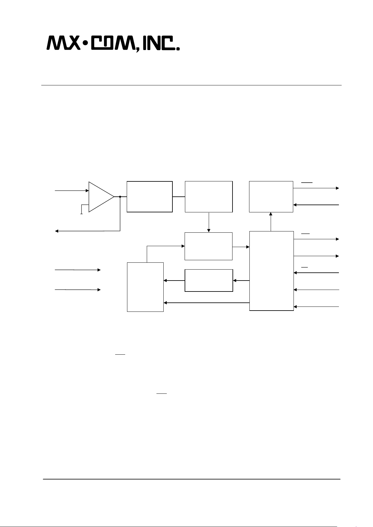
DIGITAL FILTER
FREQUENCY
ASSESSMENT AND
MEASUREMENT
SEQUENCER
AND COMPARE
C-BUS
INTERFACE
AND
CONTROL
LOGIC
XTAL AND
CLOCKS
IRQ
COMMAND DATA
SIGNAL IN
Amplifier
ROM
RAM
V/2
DD
REPLY DATA
CS
SERIAL CLOCK
OPAMP OUT
XTAL
XTAL/ CLOCK
V
DD
V
SS
+
-
The CMX813 decodes the signaling tones for the Motorola Quick Call series, GE groups A, B and C and the
tonesets employed by the Zetron, Reach and Plectron 2-tone radio paging systems. It also decodes the tones
for Motorola 5/6-tone paging and the EIA, CCIR, ZVEI1 and EEA tonesets used for HSC radio paging and
SELCALL. A simple serial interface allows the host µC to specify the individual tone(s), or group of tones, to
be decoded from the extensive list held by the CMX813.
When the µC receives an IRQ it examines the STATUS and DECODED TONE ADDRESS Registers to
reveal the tone decoded. In 2-tone mode, the CMX813 will report which of the (up to eight) selected tones it
has decoded. This report is an 8-bit index number to the tone in the programmed list. For 5/6-tone or HSC
groups, the CMX813 will report which tone in the selected system toneset (e.g. CCIR, EIA) has been
decoded, as a 4-bit hexadecimal tone value within the selected group.
To allow for cadence measurements, the
IRQ is activated again when the tone is no longer present. A status
value of “No-tone” is returned. The CMX813 is designed to operate over a wide temperature range with a
typical operating current of 0.5mA at 2.7Volts. It also has a Zero-Power mode and is available in
16-pin TSSOP (CMX813E4) and 16-pin DIP (CMX813P3) packages.
Page 2

CMX813 Multi-Standard Analog Paging Decoder 2 CMX813 Advance Information
¤
¤¤
¤2000 MX-COM, Inc. www.mxcom.com tel: 336 744 5050 800 638 5577 fax: 336 744 5054 Doc. # 20480220.002
4800 Bethania Station Road, Winston-Salem, NC 27105-1201, USA All trademarks and service mark s are held by their res pec t ive customers.
CONTENTS
Section Page
1. Block Diagram............................................................................................................... 3
2. Signal List...................................................................................................................... 4
3. External Components...................................................................................................5
4. General Description...................................................................................................... 5
5. Software Description.................................................................................................... 6
5.1 Address/Commands.............................................................................................................6
5.1.1 8-bit Write Only Registers....................................................................................................... 6
5.1.2 Write Only Register Description.............................................................................................. 6
5.1.3 8-bit Read Only Registers......................................................................................................8
5.1.4 Read Only Register Description ............................................................................................. 8
6. Application Notes.......................................................................................................... 9
6.1 General.................................................................................................................................9
6.2 Tone Ta b l es........................................................................................................................10
7. Performance Specification......................................................................................... 16
7.1 Electrical Performance........................................................................................................16
7.1.1 Absolute Maximum Ratings.................................................................................................. 16
7.1.2 Operating Limits....................................................................................................................16
7.1.3 1.7.1.3 Operating Characteristics......................................................................................... 17
7.1.4 Timing................................................................................................................................... 18
7.2 Packaging...........................................................................................................................19
MXCOM, Inc. reserves the right to change specifications at any time and without notice.
Page 3
CMX813 Multi-Standard Analog Paging Decoder 3 CMX813 Advance Information
¤
¤¤
¤2000 MX-COM, Inc. www.mxcom.com tel: 336 744 5050 800 638 5577 fax: 336 744 5054 Doc. # 20480220.002
4800 Bethania Station Road, Winston-Salem, NC 27105-1201, USA All trademarks and service mark s are held by their res pec t ive customers.
1. Block Diagram
DIGITAL FILTER
FREQUENCY
ASSESSMENT AND
MEASUREMENT
SEQUENCER
AND COMPARE
C-BUS
INTERFACE
AND
CONTROL
LOGIC
XTAL AND
CLOCKS
IRQ
COMMAND DATA
SIGNAL IN
Amplifier
ROM
RAM
V/2
DD
REPLY DATA
CS
SERIAL CLOCK
OPAMP OUT
XTAL
XTAL/ CLOCK
V
DD
V
SS
+
-
Figure 1: Block Diagram
Page 4
CMX813 Multi-Standard Analog Paging Decoder 4 CMX813 Advance Information
¤
¤¤
¤2000 MX-COM, Inc. www.mxcom.com tel: 336 744 5050 800 638 5577 fax: 336 744 5054 Doc. # 20480220.002
4800 Bethania Station Road, Winston-Salem, NC 27105-1201, USA All trademarks and service mark s are held by their res pec t ive customers.
2. Signal List
Package Signal Description
Pin No.
E4/P3
Name Type
1 SERIAL CLOCK input The C-BUS serial clock input. This clock, produced by the
µController, is used for transfer timing of commands and data
to and from the device. See Figure 3.
2 COMMAND DATA input The C-BUS serial data input from the µController. Data is
loaded into this device in 8-bit bytes, MSB (D7) first, and LSB
(D0) last, synchronized to the SERIAL CLOCK. See Figure 3.
3 REPLY DATA output The C-BUS serial data output to the µController. The
transmission of REPLY DATA bytes is synchronized to the
SERIAL CLOCK under the control of the
CS input. This 3-
state output is held at high impedance when not sending data
to the µController. See Figure 3.
4
CS
input The C-BUS data loading control function: this input is provided
by the µController. Data transfer sequences are initiated,
completed or aborted by the
CSsignal. See Figure 3.
5
IRQ
output This output indicates an interrupt condition to the µController
by going to a logic "0". This is a "wire-ORable" output;
enabling the connection of up to 8 peripherals to 1 interrupt
port on the µController. This pin has a low impedance pulldown to logic "0" when active and a high-impedance when
inactive. An external pull-up resistor is required.
An interrupt is effective if not masked out by the IRQ MASK
(bit 0 in the SUB-AUDIO CONTROL register $80).
6 NC Reserved for future use. Do not make any connection to this
pin.
7 NC For manufacturer's use only. Connect to VSS.
8 VSS power The negative supply rail (ground).
9 SIGNAL IN input The inverting input to the input amplifier.
10 OPAMP OUT output The output of the input amplifier and the input to the Digital
filter section.
11 NC
12 NC
13 NC
Reserved for future use.
Do not make any connection to these pins.
14 XTAL input The input of the on-chip oscillator.
15
XTAL
output The inverted output of the on-chip oscillator.
16 V
DD
power The positive supply rail. Levels and voltages are dependent
upon this supply. This pin should be decoupled to V
SS
by a
capacitor.
Table 1: Signal List
Page 5
CMX813 Multi-Standard Analog Paging Decoder 5 CMX813 Advance Information
¤
¤¤
¤2000 MX-COM, Inc. www.mxcom.com tel: 336 744 5050 800 638 5577 fax: 336 744 5054 Doc. # 20480220.002
4800 Bethania Station Road, Winston-Salem, NC 27105-1201, USA All trademarks and service mark s are held by their res pec t ive customers.
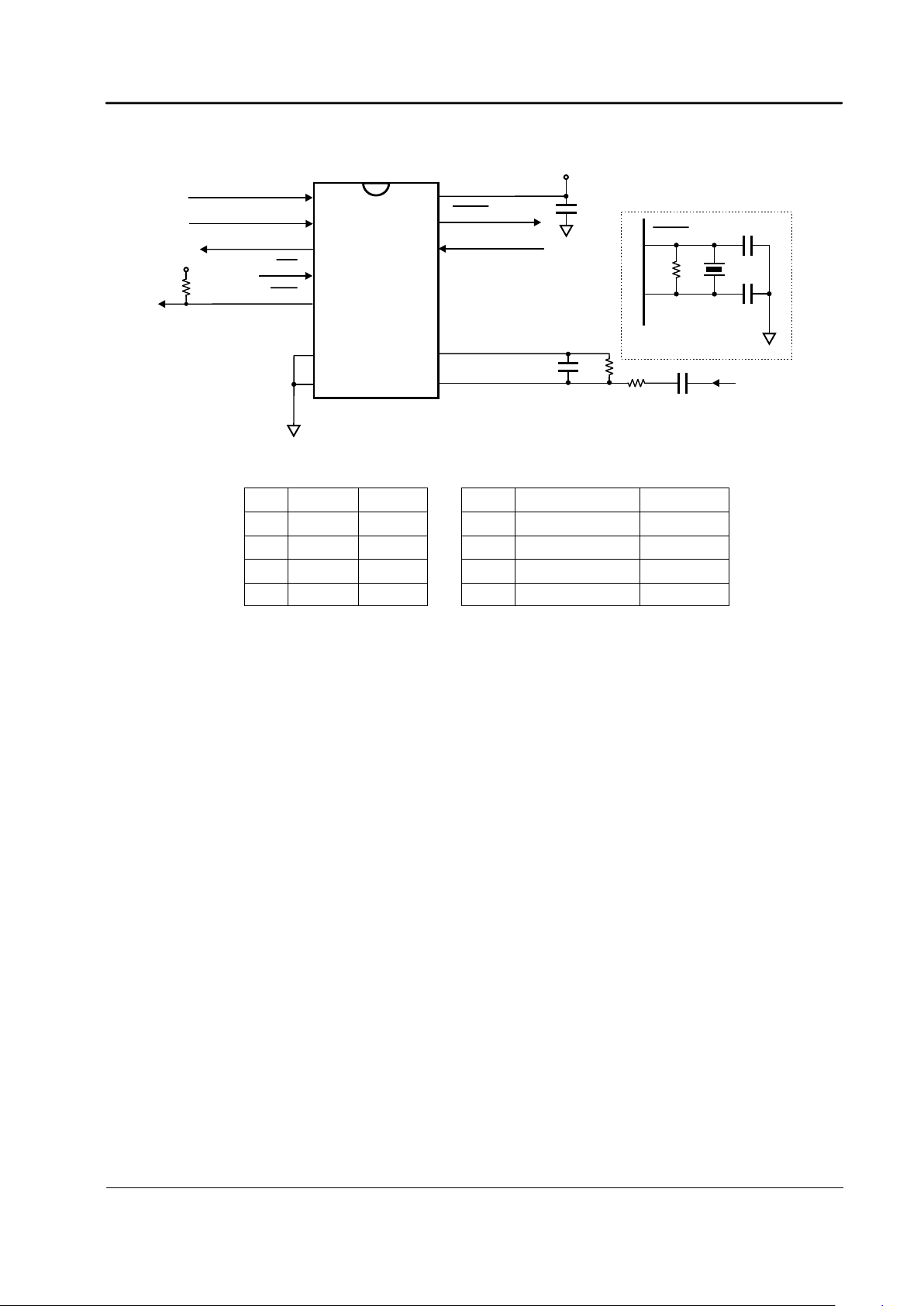
3. External Components
16
15
14
13
12
11
10
9
1
2
3
4
5
6
7
8
XTAL/CLOCK
XTAL
IRQ
SERIAL CLOCK
REPLY DATA
COMMAND DATA
CS
AMPOUT
see inset
inset
SIGNAL IN
X1
R2
C1
C2
C3
C4
V
SS
V
DD
V
DD
V
DD
CMX813
R1
XTAL
XTAL/CLOCK
15
14
R3
R4
C5
Figure 2: Recommended External Components
C1 18pF ±20% R1
1M
Ω
±5%
C2 18pF ±20% R2
22k
Ω
±10%
C3 68nF ±20% R3
1M
Ω
±10%
C4 0.1µF ±20% R4
51k
Ω
±10%
C5 22pF ±20% X1 3.5795450MHz ±100ppm
Table 2: Recommended External Components
4. General Description
When the CMX813 detects the start of a tone, it generates an interrupt and reports which tone was detected.
At the end of the tone, it will produce an interrupt and report Notone detected. The host micro should measure
and interpret the tone lengths and gap lengths according to calling code requirements. The device is not
designed for the decoding of multiple tones that are present simultaneously.
In 2-tone mode, the parameters for decoding each tone in the tone table are stored in a decoding ROM, and
any one of these tones can be selected for decoding via an 8-bit ROM address. Up to eight 8-bit ROM
addresses can be selected by the host micro for decoding. These are held in an internal address RAM which
downloads the addresses sequentially to the ROM and retrieves the tone decode parameters and matches
these with the received signal to a find tone decode. If a match is found, the CMX813 generates an interrupt
and reports the decoded tone table ROM address. The device can therefore decode any number of single or
2-tone pager codes, formed by any combination of up to 8 different frequencies, received in any order.
In 5/6 tone and HSC modes, the tone parameters are stored in ROM in groups of 16 tones in accordance with
the various international tonesets (CCIR/ZVEI etc.). Any one of these groups can be selected for decoding at
any time. ROM address sequencing is automatic. When any one of the 16 tones in that group is decoded, the
device interrupts and reports the group and tone number of the tone (8 bits).
The input amplifier with suitable external components is used to adjust the received signal to the correct
amplitude for the decoder. All functions are controlled over a C-BUS serial
µC interface.
Page 6
CMX813 Multi-Standard Analog Paging Decoder 6 CMX813 Advance Information
¤
¤¤
¤2000 MX-COM, Inc. www.mxcom.com tel: 336 744 5050 800 638 5577 fax: 336 744 5054 Doc. # 20480220.002
4800 Bethania Station Road, Winston-Salem, NC 27105-1201, USA All trademarks and service mark s are held by their res pec t ive customers.
5. Software Description
5.1 Address/Commands
Instructions and data are transferred, via C-BUS, in accordance with the timing information provided in
Figure 3.
Instruction and data transactions to and from the CMX813 consist of an Address/Command (A/C) byte, which
may be followed by either:
(i) a further instruction or data (1 byte) or
(ii) a status or Rx data reply (1 byte)
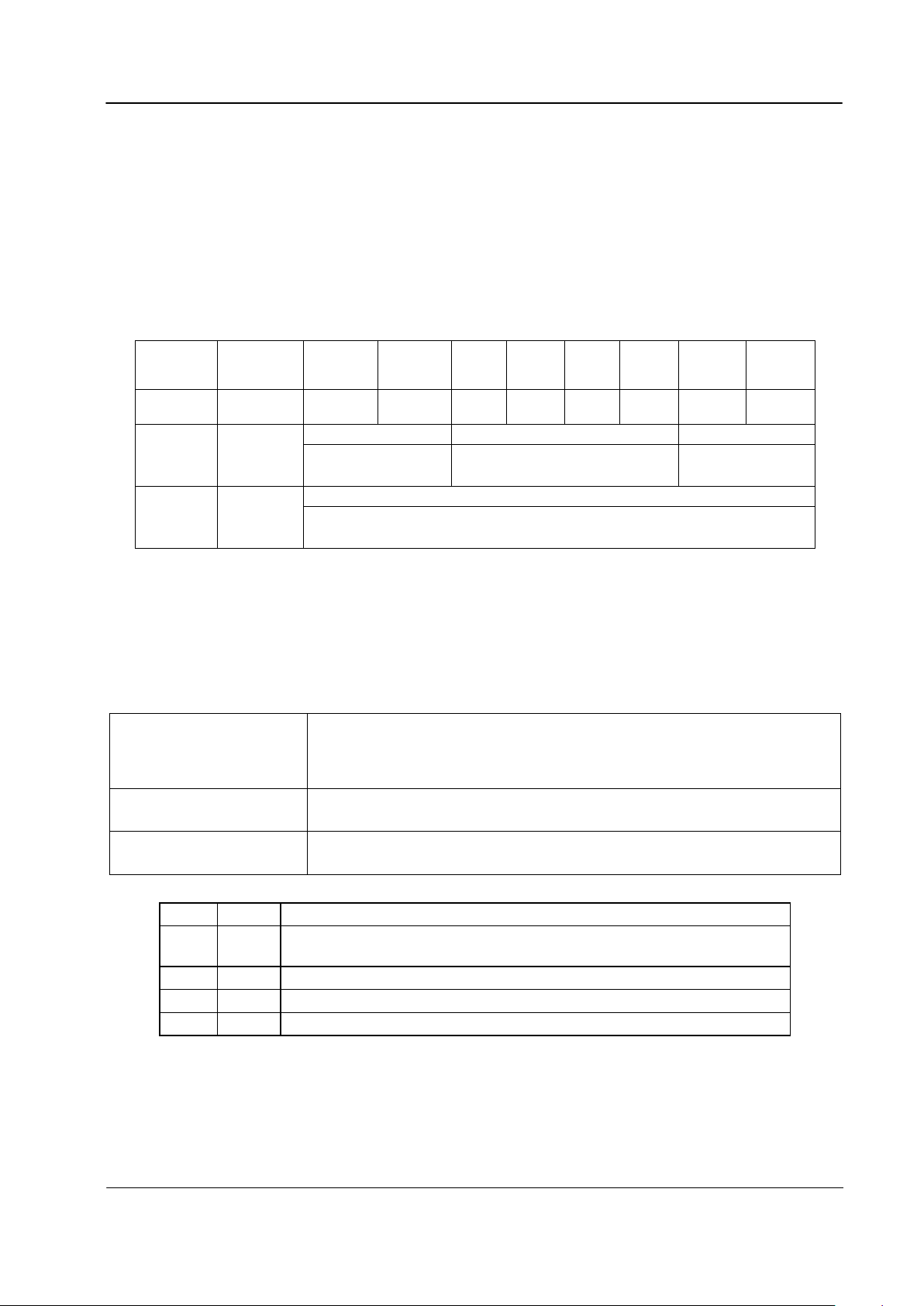
5.1.1 8-bit Write Only Registers
HEX
ADDRESS/
COMMAND
REGISTER
NAME
BIT 7
(D7)
BIT 6
(D6)
BIT 5
(D5)
BIT 4
(D4)
BIT 3
(D3)
BIT 2
(D2)
BIT 1
(D1)
BIT 0
(D0)
$01
GENERAL
RESET
N/A N/A N/A N/A N/A N/A N/A N/A
ROM PAGE SELECT DECODER BANDWIDTH OPERATION MODE
MSB LSB MSB LSB MSB LSB
$30 CONTROL
BIT 7 BIT 6 BIT 5 BIT 4 BIT 3 BIT 2 BIT 1 BIT 0
TONE ADDRESS
MSB LSB
$31
TONE
ADDRESS
BIT 7 BIT6 BIT 5 BIT 4 BIT 3 BIT 2 BIT 1 BIT 0
5.1.2 Write Only Register Description
5.1.2.1 GENERAL RESET (Hex address $01)
The reset command has no data attached to it. It sets the device (write) registers to zero and enters the Zero
Power mode. And all RAM contents and RAM FULL bit of the STATUS Register are reset to 0.
5.1.2.2 CONTROL Register (Hex address $30)
This register is used to control the functions of the device as described below:
ROM PAGE SELECT
(Bits 7 and 6)
These two bits select the section of the ROM where pre-programmed tone
data are stored for detection. The ROM area is divided into three sections
(pages). The 1 tone or 2 tone system tones are stored in ROM Page 1 and 2.
The 5/6 tone and HSC tones are stored in ROM Page 3.
DECODER BANDWIDTH
(Bits 5, 4, 3 and 2)
These four bits set the bandwidth of the tone decoder according to table
below:
OPERATION MODE
(Bits 1 and 0)
These two bits select the mode of operation of the device.
Bit 7 Bit 6 ROM PAGE
0 0
No ROM PAGE selected, a valid but unrecognized tone may be detected,
no interrupt generated
0 1 ROM Page 1 selected, for 1 tone or 2 tone system
1 0 ROM Page 2 selected, for 1 tone or 2 tone system
1 1 ROM Page 3 selected, for 5/6 tone or HSC tone system
Table 3: ROM PAGE SELECT (Bits 7 and 6)
Page 7

CMX813 Multi-Standard Analog Paging Decoder 7 CMX813 Advance Information
¤
¤¤
¤2000 MX-COM, Inc. www.mxcom.com tel: 336 744 5050 800 638 5577 fax: 336 744 5054 Doc. # 20480220.002
4800 Bethania Station Road, Winston-Salem, NC 27105-1201, USA All trademarks and service mark s are held by their res pec t ive customers.
BANDWIDTH
Bit 5 Bit 4 Bit 3 Bit 2
Nominal Decode
0 0 0 0
±0.1%
0 0 0 1
±0.3%
0 0 1 0
±0.5%
0 0 1 1
±0.7%
0 1 0 0
±0.9%
0 1 0 1
±1.1%
0 1 1 0
±1.3%
0 1 1 1
±1.5%
1 0 0 0
±1.7%
1 0 0 1
±1.9%
1 0 1 0
±2.1%
1 0 1 1
±2.3%
1 1 0 0
±2.5%
1 1 0 1
±2.7%
1 1 1 0
±2.9%
1 1 1 1
±3.1%
Table 4: DECODER BANDWIDTH (Bits 5,4,3,and 2)
Bit 1 Bit 0 OPERATION MODE
0 0 Zero Power
0 1 Clear RAM, all RAM contents and RAM FULL bit of the STATUS Register
are reset to 0.
1 0 Normal operation, decode enabled
1 1 Reserved
Table 5: OPERATION MODE (Bits 1 and 0)
5.1.2.3 TONE ADDRESS Register (Hex address $31)
This register is used to load ROM addresses to the internal RAM for decode as described below:
TONE ADDRESS
(Bits 7, 6, 5, 4, 3, 2, 1,
and 0)
The parameters (center frequency) for decoding each tone in the tone table are
stored in a decoding ROM, and any one of these tones can be selected for
decoding via this 8-bit ROM address. The tones table and address allocations
are listed in the Application Notes, Section 6.
For a 1-tone or 2-tone system, up to eight ROM addresses can be loaded to the
RAM for decode from a chosen ROM page. A FIFO system is used for loading
the RAM memory. If more than 8 ROM addresses were loaded to the RAM,
only the last 8 entries will be stored.
For the 5/6 tone and HSC tone system, Bits 7, 6, 5, and 4 are used to select a
specific tone set (CCIR/ZVEI etc.) for decode. The decode algorithm will search
automatically through the sixteen ROM addresses associated with the chosen
tone set.
Bits 3, 2, 1, and 0 are not used and should be set to 0.
Page 8

CMX813 Multi-Standard Analog Paging Decoder 8 CMX813 Advance Information
¤
¤¤
¤2000 MX-COM, Inc. www.mxcom.com tel: 336 744 5050 800 638 5577 fax: 336 744 5054 Doc. # 20480220.002
4800 Bethania Station Road, Winston-Salem, NC 27105-1201, USA All trademarks and service mark s are held by their res pec t ive customers.
5.1.3 8-bit Read Only Registers
HEX
ADDRESS/
COMMAND
REGISTER
NAME
BIT 7
(D7)
BIT 6
(D6)
BIT 5
(D5)
BIT 4
(D4)
BIT 3
(D3)
BIT 2
(D2)
BIT 1
(D1)
BIT 0
(D0)
DECODED TONE ADDRESS
MSB LSB
$38
DECODED
TONE
ADDRESS
BIT 7 BIT6 BIT 5 BIT 4 BIT 3 BIT 2 BIT 1 BIT 0
Reserved set to DECODED ROM PAGE
1 1 0 MSB LSB
$3F STATUS
RAM
FULL
DECODE
STATUS
CHANGE
TONE
DECODE
BIT 1 BIT 0
5.1.4 Read Only Register Description
5.1.4.1 DECODED TONE ADDRESS Register (Hex address $38)
This register is used to send the decoded ROM addresses to the host micro as described below:
DECODED
TONE ADDRESS
(Bits 7, 6, 5, 4, 3, 2, 1,
and 0)
When a tone is decoded, the CMX813 generates an interrupt and reports the
decoded tone table 8-bit ROM address. The tone table and address allocations
are listed in the Application Notes, Section 1.6.
For the 1-tone or 2-tone system, the 8-bit ROM address is located either from
ROM PAGE 1 or 2.
For the 5/6 tone and HSC tones system, Bits 7, 6, 5, and 4 represent the
selected tone set (CCIR/ZVEI etc), Bits 3, 2, 1, and 0 are the 4 bit Hexadecimal
tone value within the selected group. This is located in ROM PAGE 3.
5.1.4.2 STATUS Register (Hex address $3F)
This register is used to indicate the status of the device as described below:
(Bits 7, 6 and 5)
Reserved for future use. These will be set to "110" respectively but should be
ignored by user's software.
RAM FULL
(Bit 4)
After eight tone addresses are loaded to the RAM for tones located in ROM
PAGE 1 or 2, this bit is set to ‘1’. A Clear RAM command will reset it to ‘0’.
DECODE STATUS
CHANGE
(Bit 3)
When TONE DECODE (Bit 2 of this register) or the decoded 8 bit address in
DECODED TONE ADDRESS Register $38 changes state this bit will be set to
"1". A “0” indicates no decode status change.
TONE DECODE
(Bit 2)
This bit indicates the status of the tone decoder. A "1" indicates a tone has been
detected (TONE DECODE) and a "0" indicates the loss of the tone (NOTONE).
TONE DECODE means that a tone has been decoded and its characteristics
are as defined by the bandwidth (see CONTROL Register $30, Bits 5, 4, 3 and
2) and the center frequency (see TONE ADDRESS Register $31, Bit 7 to Bit 0).
When Bit 7 and Bit 6 in the CONTROL Register $30 are set to "0" the TONE
DECODE Bit 2 will be set to "0".
From NOTONE state, identification of a valid tone which is not in the pre-
programmed list (up to eight tones in 1 or 2 tone system and 16 tones in 5/6
tone or HSC) will cause the decoder to move to the TONE DECODE state with
the DECODED ROM PAGE address of "00" in Bits 1 and 0; indicating a valid but
unrecognized tone. No interrupt is generated.
Loss of tone will cause the NOTONE timer to be started. If loss of tone
continues for the duration of the time-out period, then the decoder will move to
the NOTONE state and the identification of pre-programmed tones will start
again. The time-out period is not user adjustable.
DECODED ROM
PAGE
(Bits 1 and 0)
These two bits represent the ROM PAGE where the decoded tone is located.
Page 9

CMX813 Multi-Standard Analog Paging Decoder 9 CMX813 Advance Information
¤
¤¤
¤2000 MX-COM, Inc. www.mxcom.com tel: 336 744 5050 800 638 5577 fax: 336 744 5054 Doc. # 20480220.002
4800 Bethania Station Road, Winston-Salem, NC 27105-1201, USA All trademarks and service mark s are held by their res pec t ive customers.
Bit 1 Bit 0 DECODED ROM PAGE
0 0 A valid but unrecognized tone
0 1 Decoded tone in ROM Page 1
1 0 Decoded tone in ROM Page 2
1 1 Decoded tone in ROM Page 3
Table 6: DECODED ROM PAGE (Bits 1 and 0)
If the DECODE STATUS CHANGE (Bit 3) of the STATUS Register is ‘1’ or the RAM FULL (Bit 4) of the
STATUS Register changes from ‘0’ to ‘1’ then the
IRQ output will be pulled low.
Reading the STATUS register, clears the interrupt (
IRQ output pulled high) and also, clears Bit 3 of the
STATUS Register, if set. A Clear RAM command clears Bit 4 of the STATUS Register, if set.
In Zero Power mode, Status Register Bits 7 to 0 are preset to “110x0000” respectively. RAM FULL (Bit 4)
remains undisturbed.
6. Application Notes
6.1 General
The device should be reset first by the command GENERAL RESET $01.
The decoder should then be set up according to the desired characteristics. This entails setting the
DECODER BANDWIDTH and select the ROM PAGE in the CONTROL Register $30, also selecting tones in
the chosen ROM PAGE by TONE ADDRESS Register $31 (programming the center frequencies of the
desired tones).
Up to 8 tones can be programmed either from ROM PAGE 1 or ROM PAGE 2. The RAM memory location 1
is loaded first then incrementally loaded to location 8. Alternatively, a tone group can be selected from ROM
PAGE 3.
The decoder is enabled by the CONTROL Register $30.
During operation when the device is receiving, the tones are scanned in the sequence of their location; once a
tone is detected, the remaining tones are not checked.
When the decoder detects a change in its present state an interrupt will be generated. The change that
occurred can be read from Bit 3 of the STATUS Register $3F if a tone is detected. NOTONE is indicated by
Bit 2 of the same register. The ROM PAGE of that tone can be read from Bits 1 and 0 of the same register.
The interrupt is cleared by reading the STATUS Register. The decoded tone address can be read from the
DECODED TONE ADDRESS Register $38
Page 10

CMX813 Multi-Standard Analog Paging Decoder 10 CMX813 Advance Information
¤
¤¤
¤2000 MX-COM, Inc. www.mxcom.com tel: 336 744 5050 800 638 5577 fax: 336 744 5054 Doc. # 20480220.002
4800 Bethania Station Road, Winston-Salem, NC 27105-1201, USA All trademarks and service mark s are held by their res pec t ive customers.
6.2 Tone Tables
The tables on the following pages list the commonly used paging tones and the corresponding ROM address
for programming the TONE ADDRESS Register $31.
ROM PAGE 1 ROM PAGE 2
D7 D6 D5 D4 D3 D2 D1 D0 Hex
System Tone # Freq. System Tone # Chnl. Freq.
0 0 0 0 0 0 0 0 00 Reach 0 Reserved
0 0 0 0 0 0 0 1 01 Mot.1 0 330.5 Single 1 Reserved
0 0 0 0 0 0 1 0 02 1 349 Tone 2 Reserved
0 0 0 0 0 0 1 1 03 2 368.5 3 Reserved
0 0 0 0 0 1 0 0 04 3 389 4 3446
0 0 0 0 0 1 0 1 05 4 410.8 5 3329
0 0 0 0 0 1 1 0 06 5 433.7 6 3215
0 0 0 0 0 1 1 1 07 6 457.9 7 3106
0 0 0 0 1 0 0 0 08 7 483.5 8 3000
0 0 0 0 1 0 0 1 09 8 510.5 9 2898
0 0 0 0 1 0 1 0 0A 9 539 10 2799
0 0 0 0 1 0 1 1 0B Diag. 569.1 Reach 1 11 2704
0 0 0 0 1 1 0 0 0C Mot. 2 0 569.1 Group A 2 12 2612
0 0 0 0 1 1 0 1 0D 1 600.9 3 13 2523
0 0 0 0 1 1 1 0 0E 2 634.5 4 14 2437
0 0 0 0 1 1 1 1 0F 3 669.9 5 15 2354
0 0 0 1 0 0 0 0 10 4 707.3 6 16 2274
0 0 0 1 0 0 0 1 11 5 746.8 7 17 2196
0 0 0 1 0 0 1 0 12 6 788.5 8 18 2121
0 0 0 1 0 0 1 1 13 7 832.5 9 19 2049
0 0 0 1 0 1 0 0 14 8 879 0 20 1980
0 0 0 1 0 1 0 1 15 9 928.1 Reach 1 21 1912
0 0 0 1 0 1 1 0 16 Diag. 979.9 Group B 2 22 1847
0 0 0 1 0 1 1 1 17 Mot. 3 0 1092.4 3 23 1784
0 0 0 1 1 0 0 0 18 1 288.5 4 24 1723
0 0 0 1 1 0 0 1 19 2 296.5 5 25 1664
0 0 0 1 1 0 1 0 1A 3 304.7 6 26 1608
0 0 0 1 1 0 1 1 1B 4 313 7 27 1553
0 0 0 1 1 1 0 0 1C 5 953.7 8 28 1500
0 0 0 1 1 1 0 1 1D 6 979.9 9 29 1449
0 0 0 1 1 1 1 0 1E 7 1006.9 0 30 1400
0 0 0 1 1 1 1 1 1F 8 1034.7 Reach 1 31 1352
0 0 1 0 0 0 0 0 20 9 1063.2 Group C 2 32 1306
0 0 1 0 0 0 0 1 21 Diag. 569.1 3 33 1261
0 0 1 0 0 0 1 0 22 Mot. 4 0 321.7 4 34 1219
0 0 1 0 0 0 1 1 23 1 339.6 5 35 1177
0 0 1 0 0 1 0 0 24 2 358.6 6 36 1137
0 0 1 0 0 1 0 1 25 3 378.6 7 37 1098
0 0 1 0 0 1 1 0 26 4 399.8 8 38 1061
0 0 1 0 0 1 1 1 27 5 422.1 9 39 1025
0 0 1 0 1 0 0 0 28 6 445.7 0 40 990
0 0 1 0 1 0 0 1 29 7 470.5 Reach 1 41 956
0 0 1 0 1 0 1 0 2A 8 496.8 Group D 2 42 923
0 0 1 0 1 0 1 1 2B 9 524.6 3 43 892
0 0 1 0 1 1 0 0 2C Diag. 569.1 4 44 862
Page 11

CMX813 Multi-Standard Analog Paging Decoder 11 CMX813 Advance Information
¤
¤¤
¤2000 MX-COM, Inc. www.mxcom.com tel: 336 744 5050 800 638 5577 fax: 336 744 5054 Doc. # 20480220.002
4800 Bethania Station Road, Winston-Salem, NC 27105-1201, USA All trademarks and service mark s are held by their res pec t ive customers.
ROM PAGE 1 ROM PAGE 2
D7 D6 D5 D4 D3 D2 D1 D0 Hex
System Tone # Freq. System Tone # Chnl. Freq.
0 0 1 0 1 1 0 1 2D Mot. 5 0 553.9 Reach 5 45 832
0 0 1 0 1 1 1 0 2E 1 584.8 Group D 6 46 804
0 0 1 0 1 1 1 1 2F 2 617.4 continue 7 47 776
0 0 1 1 0 0 0 0 30 3 651.9 8 48 750
0 0 1 1 0 0 0 1 31 4 688.3 9 49 725
0 0 1 1 0 0 1 0 32 5 726.8 0 50 700
0 0 1 1 0 0 1 1 33 6 767.4 1 51 676
0 0 1 1 0 1 0 0 34 7 810.2 Reach 2 52 653
0 0 1 1 0 1 0 1 35 8 855.5 Group E 3 53 631
0 0 1 1 0 1 1 0 36 9 903.2 4 54 609
0 0 1 1 0 1 1 1 37 Diag. 979.9 5 55 588
0 0 1 1 1 0 0 0 38 Mot. 6 0 1122.5 6 57 549
0 0 1 1 1 0 0 1 39 1 1153.4 7 58 530
0 0 1 1 1 0 1 0 3A 2 1185.2 8 59 512
0 0 1 1 1 0 1 1 3B 3 1217.8 9 60 495
0 0 1 1 1 1 0 0 3C 4 1251.4 0 0 1 1 1 1 0 1 3D 5 1285.8 0 0 1 1 1 1 1 0 3E 6 1321.2 0 0 1 1 1 1 1 1 3F 7 1357.6 0 1 0 0 0 0 0 0 40 8 1395 0 1 0 0 0 0 0 1 41 9 1433.4 -
ROM PAGE 1 ROM PAGE 2
D7 D6 D5 D4 D3 D2 D1 D0 Hex
System Tone # Freq. System Tone # Freq.
0 1 0 0 0 0 1 0 42 Diag. 979.9 Plectron 0 282.2
0 1 0 0 0 0 1 1 43 Mot. 10 0 1472.9 1 294.7
0 1 0 0 0 1 0 0 44 1 1513.5 2 307.8
0 1 0 0 0 1 0 1 45 2 1555.2 3 321.4
0 1 0 0 0 1 1 0 46 3 1598 4 335.6
0 1 0 0 0 1 1 1 47 4 1642 5 350.5
0 1 0 0 1 0 0 0 48 5 1687.2 6 366
0 1 0 0 1 0 0 1 49 6 1733.7 7 382.3
0 1 0 0 1 0 1 0 4A 7 1781.5 8 399.2
0 1 0 0 1 0 1 1 4B 8 1830.5 9 416.9
0 1 0 0 1 1 0 0 4C 9 1881 10 435.3
0 1 0 0 1 1 0 1 4D Mot. 11 0 1930.2 11 454.6
0 1 0 0 1 1 1 0 4E 1 1989 12 474.8
0 1 0 0 1 1 1 1 4F 2 2043.8 13 495.8
0 1 0 1 0 0 0 0 50 3 2094.5 14 517.8
0 1 0 1 0 0 0 1 51 4 2155.6 15 540.7
0 1 0 1 0 0 1 0 52 5 2212.2 16 564.7
0 1 0 1 0 0 1 1 53 6 2271.7 17 589.7
0 1 0 1 0 1 0 0 54 7 2334.6 18 615.8
0 1 0 1 0 1 0 1 55 8 2401 19 643
Page 12

CMX813 Multi-Standard Analog Paging Decoder 12 CMX813 Advance Information
¤
¤¤
¤2000 MX-COM, Inc. www.mxcom.com tel: 336 744 5050 800 638 5577 fax: 336 744 5054 Doc. # 20480220.002
4800 Bethania Station Road, Winston-Salem, NC 27105-1201, USA All trademarks and service mark s are held by their res pec t ive customers.
ROM PAGE 1 ROM PAGE 2
D7 D6 D5 D4 D3 D2 D1 D0 Hex
System Tone # Freq. System Tone # Freq.
0 1 0 1 0 1 1 0 56 9 2468.2 Plectron 20 672
0 1 0 1 0 1 1 1 57 GE. A 0 682.5 continue 21 701
0 1 0 1 1 0 0 0 58 1 592.5 22 732
0 1 0 1 1 0 0 1 59 2 757.5 23 765
0 1 0 1 1 0 1 0 5A 3 802.5 24 799
0 1 0 1 1 0 1 1 5B 4 847.5 25 834
0 1 0 1 1 1 0 0 5C 5 892.5 26 871
0 1 0 1 1 1 0 1 5D 6 937.5 27 910
0 1 0 1 1 1 1 0 5E 7 547.5 28 950
0 1 0 1 1 1 1 1 5F 8 727.5 29 992
0 1 1 0 0 0 0 0 60 9 637.5 30 1036
0 1 1 0 0 0 0 1 61 Diag. 742.5 31 1082
0 1 1 0 0 0 1 0 62 GE. B 0 652.5 32 1130
0 1 1 0 0 0 1 1 63 1 607.5 33 1180
0 1 1 0 0 1 0 0 64 2 787.5 34 1232
0 1 1 0 0 1 0 1 65 3 832.5 35 1287
0 1 1 0 0 1 1 0 66 4 877.5 36 1344
0 1 1 0 0 1 1 1 67 5 922.5 37 1403
0 1 1 0 1 0 0 0 68 6 967.5 38 1465
0 1 1 0 1 0 0 1 69 7 517.5 39 1530
0 1 1 0 1 0 1 0 6A 8 562.5 40 1598
0 1 1 0 1 0 1 1 6B 9 697.5 41 1669
ROM PAGE 1 ROM PAGE 2
D7 D6 D5 D4 D3 D2 D1 D0 Hex
System Tone # Freq. System Tone # Freq.
0 1 1 0 1 1 0 0 6C Diag. 742.5 Plectron 42 1743
0 1 1 0 1 1 0 1 6D GE. C 0 667.5 continue 43 1820
0 1 1 0 1 1 1 0 6E 1 712.5 44 1901
0 1 1 0 1 1 1 1 6F 2 772.5 45 1985
0 1 1 1 0 0 0 0 70 3 817.5 46 2073
0 1 1 1 0 0 0 1 71 4 862.5 47 2164
0 1 1 1 0 0 1 0 72 5 907.5 48 2260
0 1 1 1 0 0 1 1 73 6 952.5 49 2361
0 1 1 1 0 1 0 0 74 7 532.5 50 2465
0 1 1 1 0 1 0 1 75 8 577.5 51 2575
0 1 1 1 0 1 1 0 76 9 622.5 52 2688
0 1 1 1 0 1 1 1 77 Diag. 742.5 53 2807
0 1 1 1 1 0 0 0 78 Mot. A 0 358.9 54 2932
0 1 1 1 1 0 0 1 79 1 398.1 55 3062
0 1 1 1 1 0 1 0 7A 2 441.6 56 3197
0 1 1 1 1 0 1 1 7B 3 489.8 57 3339
0 1 1 1 1 1 0 0 7C 4 543.3 58 3487
0 1 1 1 1 1 0 1 7D 5 602.6 59 1957
0 1 1 1 1 1 1 0 7E 6 668.3 0 1 1 1 1 1 1 1 7F 7 741.3 -
Page 13

CMX813 Multi-Standard Analog Paging Decoder 13 CMX813 Advance Information
¤
¤¤
¤2000 MX-COM, Inc. www.mxcom.com tel: 336 744 5050 800 638 5577 fax: 336 744 5054 Doc. # 20480220.002
4800 Bethania Station Road, Winston-Salem, NC 27105-1201, USA All trademarks and service mark s are held by their res pec t ive customers.
ROM PAGE 1 ROM PAGE 3
D7 D6 D5 D4 D3 D2 D1 D0 Hex
System Tone # Freq. System Tone # Freq.
1 0 0 0 0 0 0 0 80 8 822.2 EIA 0 600
1 0 0 0 0 0 0 1 81 Mot. A 9 912 1 741
1 0 0 0 0 0 1 0 82 continue A 1011.6 2 882
1 0 0 0 0 0 1 1 83 B 1122.1 3 1023
1 0 0 0 0 1 0 0 84 Diag. 979.9 4 1164
1 0 0 0 0 1 0 1 85 Mot. B 0 371.5 5 1305
1 0 0 0 0 1 1 0 86 1 412.1 6 1446
1 0 0 0 0 1 1 1 87 2 457.1 7 1587
1 0 0 0 1 0 0 0 88 3 507 8 1728
1 0 0 0 1 0 0 1 89 4 562.3 9 1869
1 0 0 0 1 0 1 0 8A 5 623.7 A 2151
1 0 0 0 1 0 1 1 8B 6 691.8 B 2435
1 0 0 0 1 1 0 0 8C 7 767.4 X/C 2010
1 0 0 0 1 1 0 1 8D 8 851.1 D 2295
1 0 0 0 1 1 1 0 8E 9 944.1 R/E 459
1 0 0 0 1 1 1 1 8F A 1047.1 F 1 0 0 1 0 0 0 0 90 B 1161.4 CCIR 0 1981
1 0 0 1 0 0 0 1 91 Diag. 979.9 1 1124
1 0 0 1 0 0 1 0 92 Mot. Z 0 346.7 2 1197
1 0 0 1 0 0 1 1 93 1 384.6 3 1275
1 0 0 1 0 1 0 0 94 2 426.6 4 1358
1 0 0 1 0 1 0 1 95 3 473.2 5 1446
1 0 0 1 0 1 1 0 96 4 524.8 6 1540
1 0 0 1 0 1 1 1 97 5 582.1 7 1640
1 0 0 1 1 0 0 0 98 6 645.7 8 1747
1 0 0 1 1 0 0 1 99 7 716.1 9 1860
1 0 0 1 1 0 1 0 9A 8 794.3 A 2400
1 0 0 1 1 0 1 1 9B 9 881 B 930
1 0 0 1 1 1 0 0 9C A 977.2 X/C 2247
1 0 0 1 1 1 0 1 9D B 1084 D 991
1 0 0 1 1 1 1 0 9E Diag. 979.9 R/E 2110
1 0 0 1 1 1 1 1 9F Zetron 1980 F 1055
1 0 1 0 0 0 0 0 A0 Grp. 1 2704 ZVEI1 0 2400
1 0 1 0 0 0 0 1 A1 2612 1 1060
1 0 1 0 0 0 1 0 A2 2523 2 1160
1 0 1 0 0 0 1 1 A3 2437 3 1270
1 0 1 0 0 1 0 0 A4 2354 4 1400
1 0 1 0 0 1 0 1 A5 2274 5 1530
1 0 1 0 0 1 1 0 A6 2196 6 1670
1 0 1 0 0 1 1 1 A7 2121 7 1830
1 0 1 0 1 0 0 0 A8 2049 8 2000
1 0 1 0 1 0 0 1 A9 Grp. 2 1177 9 2200
1 0 1 0 1 0 1 0 AA 1608 A 2800
1 0 1 0 1 0 1 1 AB 1553 B 810
1 0 1 0 1 1 0 0 AC 1500 X/C 970
Page 14

CMX813 Multi-Standard Analog Paging Decoder 14 CMX813 Advance Information
¤
¤¤
¤2000 MX-COM, Inc. www.mxcom.com tel: 336 744 5050 800 638 5577 fax: 336 744 5054 Doc. # 20480220.002
4800 Bethania Station Road, Winston-Salem, NC 27105-1201, USA All trademarks and service mark s are held by their res pec t ive customers.
ROM PAGE 1 ROM PAGE 3
D7 D6 D5 D4 D3 D2 D1 D0 Hex
System Tone # Freq. System Tone # Freq.
1 0 1 0 1 1 0 1 AD 1449 ZVEI1 D 885
1 0 1 0 1 1 1 0 AE Zetron 1400 continue R/E 2600
1 0 1 0 1 1 1 1 AF Grp. 2 1352 F 680
1 0 1 1 0 0 0 0 B0 continue 1306 ZVEI2 0 2400
1 0 1 1 0 0 0 1 B1 1261 1 1060
1 0 1 1 0 0 1 0 B2 1219 2 1160
1 0 1 1 0 0 1 1 B3 Grp. 3 1400 3 1270
1 0 1 1 0 1 0 0 B4 1912 4 1400
1 0 1 1 0 1 0 1 B5 1847 5 1530
1 0 1 1 0 1 1 0 B6 1784 6 1670
1 0 1 1 0 1 1 1 B7 1723 7 1830
1 0 1 1 1 0 0 0 B8 1664 8 2000
1 0 1 1 1 0 0 1 B9 1608 9 2200
1 0 1 1 1 0 1 0 BA 1553 A 885
1 0 1 1 1 0 1 1 BB 1500 B 810
1 0 1 1 1 1 0 0 BC 1449 X/C 740
1 0 1 1 1 1 0 1 BD Grp. 4 832 D 680
1 0 1 1 1 1 1 0 BE 1137 R/E 970
1 0 1 1 1 1 1 1 BF 1098 F 2600
1 1 0 0 0 0 0 0 C0 1061 ZVEI3/ 0 2200
1 1 0 0 0 0 0 1 C1 1025 DZVEI 1 970
1 1 0 0 0 0 1 0 C2 990 2 1060
1 1 0 0 0 0 1 1 C3 956 3 1160
1 1 0 0 0 1 0 0 C4 923 4 1270
1 1 0 0 0 1 0 1 C5 892 5 1400
1 1 0 0 0 1 1 0 C6 862 6 1530
1 1 0 0 0 1 1 1 C7 Grp. 5 588 7 1670
1 1 0 0 1 0 0 0 C8 804 8 1830
1 1 0 0 1 0 0 1 C9 776 9 2000
1 1 0 0 1 0 1 0 CA 750 A 825
1 1 0 0 1 0 1 1 CB 725 B 740
1 1 0 0 1 1 0 0 CC 700 X/C 2600
1 1 0 0 1 1 0 1 CD 676 D 885
1 1 0 0 1 1 1 0 CE 653 R/E 2400
1 1 0 0 1 1 1 1 CF 631 F 680
1 1 0 1 0 0 0 0 D0 609 PZVEI 0 2400
1 1 0 1 0 0 0 1 D1 - 1 1060
1 1 0 1 0 0 1 0 D2 - 2 1160
1 1 0 1 0 0 1 1 D3 - 3 1270
1 1 0 1 0 1 0 0 D4 - 4 1400
1 1 0 1 0 1 0 1 D5 - 5 1530
1 1 0 1 0 1 1 0 D6 - 6 1670
1 1 0 1 0 1 1 1 D7 - 7 1830
1 1 0 1 1 0 0 0 D8 - 8 2000
Page 15

CMX813 Multi-Standard Analog Paging Decoder 15 CMX813 Advance Information
¤
¤¤
¤2000 MX-COM, Inc. www.mxcom.com tel: 336 744 5050 800 638 5577 fax: 336 744 5054 Doc. # 20480220.002
4800 Bethania Station Road, Winston-Salem, NC 27105-1201, USA All trademarks and service mark s are held by their res pec t ive customers.
ROM PAGE 1 ROM PAGE 3
D7 D6 D5 D4 D3 D2 D1 D0 Hex
System Tone # Freq. System Tone # Freq.
1 1 0 1 1 0 0 1 D9 - PZVEI 9 2200
1 1 0 1 1 0 1 0 DA - continue A 970
1 1 0 1 1 0 1 1 DB - B 810
1 1 0 1 1 1 0 0 DC - X/C 2800
1 1 0 1 1 1 0 1 DD - D 885
1 1 0 1 1 1 1 0 DE - R/E 2600
1 1 0 1 1 1 1 1 DF - F 680
1 1 1 0 0 0 0 0 E0 - EEA 0 1981
1 1 1 0 0 0 0 1 E1 - 1 1124
1 1 1 0 0 0 1 0 E2 - 2 1197
1 1 1 0 0 0 1 1 E3 - 3 1275
1 1 1 0 0 1 0 0 E4 - 4 1358
1 1 1 0 0 1 0 1 E5 - 5 1446
1 1 1 0 0 1 1 0 E6 - 6 1540
1 1 1 0 0 1 1 1 E7 - 7 1640
1 1 1 0 1 0 0 0 E8 - 8 1747
1 1 1 0 1 0 0 1 E9 - 9 1860
1 1 1 0 1 0 1 0 EA - A 1055
1 1 1 0 1 0 1 1 EB - B 930
1 1 1 0 1 1 0 0 EC - X/C 2247
1 1 1 0 1 1 0 1 ED - D 991
1 1 1 0 1 1 1 0 EE - R/E 2110
1 1 1 0 1 1 1 1 EF - F 2400
1 1 1 1 0 0 0 0 F0 - 1 1 1 1 0 0 0 1 F1 - 1 1 1 1 0 0 1 0 F2 - 1 1 1 1 0 0 1 1 F3 - 1 1 1 1 0 1 0 0 F4 - 1 1 1 1 0 1 0 1 F5 - 1 1 1 1 0 1 1 0 F6 - 1 1 1 1 0 1 1 1 F7 - 1 1 1 1 1 0 0 0 F8 - 1 1 1 1 1 0 0 1 F9 - 1 1 1 1 1 0 1 0 FA - 1 1 1 1 1 0 1 1 FB - 1 1 1 1 1 1 0 0 FC - 1 1 1 1 1 1 0 1 FD - 1 1 1 1 1 1 1 0 FE - 1 1 1 1 1 1 1 1 FF - -
Page 16

CMX813 Multi-Standard Analog Paging Decoder 16 CMX813 Advance Information
¤
¤¤
¤2000 MX-COM, Inc. www.mxcom.com tel: 336 744 5050 800 638 5577 fax: 336 744 5054 Doc. # 20480220.002
4800 Bethania Station Road, Winston-Salem, NC 27105-1201, USA All trademarks and service mark s are held by their res pec t ive customers.
7. Performance Specification
7.1 Electrical Performance
7.1.1 Absolute Maximum Ratings
Exceeding these maximum ratings can result in damage to the device.
Min. Max. Units
Supply (VDD - VSS) -0.3 7.0 V
Voltage on any pin to VSS -0.3 V
DD
+ 0.3 V
Current into or out of VDD and V
SS
pins -30 +30 mA
Current into or out of any other pin -20 +20 mA
E4 Package Min. Max. Units
Total Allowable Power Dissipation at T
AMB
= 25°C 300 mW
Derating above 25°C 5 mW/°C above 25°C
Storage Temperature -55 +125 °C
Operating Temperature -40 +85 °C
P3 Package
Total Allowable Power Dissipation at T
AMB
= 25°C 800 mW
Derating above 25°C 13 mW/°C above 25°C
Storage Temperature -55 +125 °C
Operating Temperature -40 +85 °C
7.1.2 Operating Limits
Correct operation of the device outside these limits is not implied.
Notes Min. Max. Units
Supply (VDD - VSS) 2.7 5.5 V
Operating Temperature -40 +85 °C
Xtal Frequency 3.579187 3.579903 MHz
Page 17

CMX813 Multi-Standard Analog Paging Decoder 17 CMX813 Advance Information
¤
¤¤
¤2000 MX-COM, Inc. www.mxcom.com tel: 336 744 5050 800 638 5577 fax: 336 744 5054 Doc. # 20480220.002
4800 Bethania Station Road, Winston-Salem, NC 27105-1201, USA All trademarks and service mark s are held by their res pec t ive customers.
7.1.3 Operating Characteristics
For the following conditions unless otherwise specified:
Xtal Frequency = 3.579545MHz. V
DD
= 2.7V to 5.5V, T
AMB
= -40°C to +85°C.
Noise Bandwidth = 5kHz Band Limited Gaussian, 0dB reference = 775mV
RMS
Notes Min. Typ. Max. Units
DC Parameters
At V
DD
= 2.7V
IDD ( Zero Power) 1 - 1.0 2.0 µA
IDD (Operating) 1 - 0.5 1.0 mA
At V
DD
= 5.0V
IDD (Zero Power) 1 - 1.0 2.0 µA
IDD (Operating) 1 - 1.0 2.0 mA
C-BUS Interface
Input Logic "1" 70% - - VDD
Input Logic "0" - - 30% VDD
Input Leakage Current (Logic "1" or "0") -1.0 - 1.0 µA
Input Capacitance - - 7.5 pF
Output Logic "1" (IOH = 360µA) 90% - - VDD
Output Logic "0" (IOL = 360µA) - - 10% VDD
IRQ output "Off" State Leakage Current (V
OUT
= VDD)
- - 1.0 µA
AC Parameters
Decoder
Sensitivity 2 - -65.0 - dB
Tone Measurement Resolution - 0.2 - %
Tone Measurement Accuracy - 0.5 - %
Response Time 2-Tone Mode 3 - 30.0 46.0 ms
De-Response Time 2-Tone Mode 3 - 76.0 82.0 ms
Response Time 5/6-Tone and HSC Mode 3 - 25.0 34.0 ms
De-Response Time 5/6-Tone and HSC Mode 3 - 43.0 62.0 ms
Frequency Range 280 - 3500 Hz
Signal/Noise 2.0 dB
Input Amplifier
Open Loop Gain (input = 1mV at 100Hz) - 70.0 - dB
Unity Gain Bandwidth - 5.0 - MHz
Input Impedance (at 100Hz) 10.0 - -
M
Ω
Output Impedance (Open Loop) - 6.0 -
k
Ω
Xtal/Clock Input
Pulse Width ('High' or 'Low') 4 40.0 - - ns
Input Impedance (at 100Hz) 10.0 - -
M
Ω
Gain (input = 1mV
RMS
at 100Hz) 20.0 - - dB
Notes:
1. Not including any current drawn from the device pins by external circuitry.
2. At V
DD
= 5.0V only. Signal levels are proportional to VDD, driven with a source impedance of <1000Ω.
3. 2-tone mode covers tones from ROM Page 1 and 2; 5/6-tone and HSC mode covers tones from ROM
Page 3. Deresponse times are for 95% probability.
4. Timing for an external input to the XTAL/CLOCK pin.
Page 18

CMX813 Multi-Standard Analog Paging Decoder 18 CMX813 Advance Information
¤
¤¤
¤2000 MX-COM, Inc. www.mxcom.com tel: 336 744 5050 800 638 5577 fax: 336 744 5054 Doc. # 20480220.002
4800 Bethania Station Road, Winston-Salem, NC 27105-1201, USA All trademarks and service mark s are held by their res pec t ive customers.
7.1.4 Timing
C-BUS Timings (See Figure 3 and Note 5) Notes Min. Typ. Max. Unit
t
CSE
CS-Enable to Clock-High time
100 - - ns
t
CSH
Last Clock-High to
CS-High time
100 - - ns
t
LOZ
Clock-Low to Reply Output enable time 0.0 - - ns
t
HIZ
CS-High to Reply Output 3-state time
- - 1.0 µs
t
CSOFF
CS-High Time between transactions
1.0 - - µs
t
NXT
Inter-Byte Time 500 - - ns
tCK Clock-Cycle time 500 - - ns
tCH Serial Clock-High time 200 - - ns
tCL Serial Clock-Low time 200 - - ns
t
CDS
Command Data Set-Up time 75 - - ns
t
CDH
Command Data Hold time 25 - - ns
t
RDS
Reply Data Set-Up time 75 - - ns
t
RDH
Reply Data Hold time 0 - - ns
CS
HI-Z
= Level not important or undefined
SERIAL CLOCK
t
CSE
t
NXT
t
CK
t
CL
t
CDH
t
RDS
t
CDH
t
RDH
70% V
DD
30% V
DD
t
CH
t
CK
t
CSOFF
t
CSH
t
HI Z
t
LOZ
COMMAND DATA
COMMAND
DATA
SERIAL
CLOCK
REPLY
DATA
REPLY DATA
76543
21
0 76543
21
0
76543
21
0
Figure 3: C-BUS Timing
Notes:
1. Depending on the command, 1 or 2 bytes of COMMAND DATA are transmitted to the
peripheral MSB (Bit 7) first, LSB (Bit 0) last. REPLY DATA is read from the peripheral MSB (Bit 7) first,
LSB (Bit 0) last.
2. Data is clocked into and out of the peripheral on the rising SERIAL CLOCK edge.
3. Loaded commands are acted upon at the end of each command.
4. To allow for differing µController serial interface formats C-BUS compatible ICs are able to work with
either polarity SERIAL CLOCK pulses.
5. These timings are for the latest version of the C-BUS as embodied in the CMX813, and allow faster
transfers than the original C-BUS timings given in MX-COM’s Publication Doc. # 20480060.001.
Page 19

CMX813 Multi-Standard Analog Paging Decoder 19 CMX813 Advance Information
¤
¤¤
¤2000 MX-COM, Inc. www.mxcom.com tel: 336 744 5050 800 638 5577 fax: 336 744 5054 Doc. # 20480220.002
4800 Bethania Station Road, Winston-Salem, NC 27105-1201, USA All trademarks and service mark s are held by their res pec t ive customers.
7.2 Packaging
Figure 4: 16-pin TSSOP (E4) Mechanical Outline: Order as part no. CMX813E4
B
M
K
K1
A
H
F
J1
J
C
PIN 1
P
L
E
Z
Y
E1
T
A
B
C
E
E1
F
H
TYP.
MAX.MIN.
DIM.
J
J1
P
Y
T
Z
K1
K
L
M
0.200 (5.08)
0.262 (6.65)
0.390 (9.91).
7°
5°
0.150 (3.81)
0.810 (20.57)
0.135 (3.43)
0.100 (2.54)
0.028 (0.71)
0.121 (3.07)
0.300 (7.62)
0.290 (7.37)
0.70 (17.78)
0.325 (8.26)
0.015 (0.38) 0.040 (1.02)
0.008 (0.20)
0.015 (0.38)
0.015 (0.38)
0.023 (0.58)
0.040 (1.02)
0.065 (1.65)
0.056 (1.42)
0.056 (1.42)
0.064 (1.63)
0.064 (1.63)
0.740 (18.80)
0.240 (6.10)
*
*
NOTE :
*
All dimensions in inches (mm.)
Angles are in degrees
A & B are reference datum's and do
not include mold deflash or protrusions.
Figure 5: 16-pin PDIP (P3) Mechanical Outline: Order as part no. CMX813P3
 Loading...