

Page 1
DATA BULLETIN
CMX808A
1999 MX-COM, Inc. www.mxcom.com tel: 800 638 5577 336 744 5050 fax: 336 744 5054 Doc. # 20480199.002
4800 Bethania Station Road, Winston-Salem, NC 27105-1201 USA All trademarks and service marks are held by their respective companies.
Family Radio Service
CTCSS Processor
PRELIMINARY INFORMATION
Features
•
Rapid multi-tone CTCSS decoder
supports new end user features
•
Fast Tone Decode (150ms)
•
Supports Tones from 62.5Hz to 251Hz
•
Integrated 32 Step Digital Volume
Control (-48.0dB to 0dB + Off)
•
Tone Cloning Capabilities
•
Sub-Audio Tone Rejection Filter
•
Low Power 3.0V to 5.5V Operation
•
Very small 20-pin TSSOP Package
•
4.0MHz Xtal/Clock Oscillator
Applications
•
Family Radio Service (FRS) Radios
•
Amateur Radio Equipment
•
General Mobile Radio Service (GMRS)
•
Short Range Business Radio
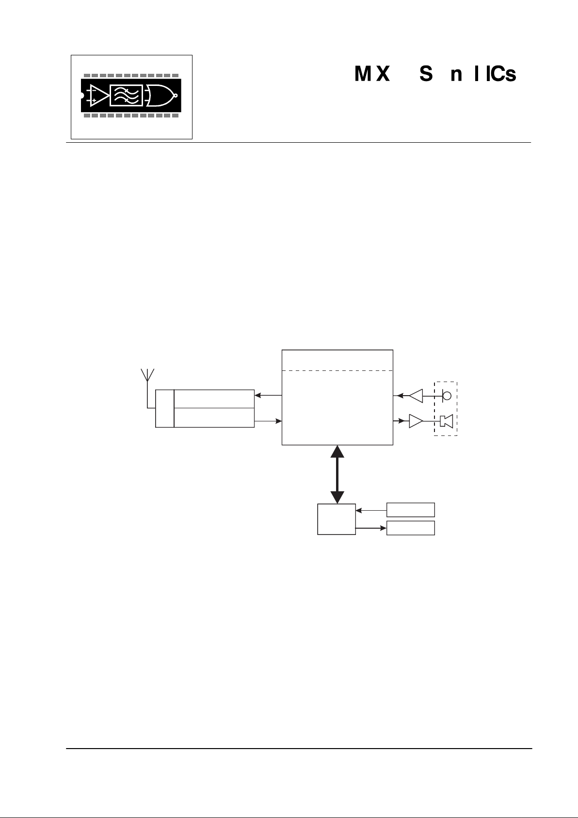
MODULATOR
DISCRIMINATOR
HOST
µC
KEYPAD
DISPLA Y
RADIO
CMX808A
RF
Tx
SERIAL 'C-BUS'
DATA & CONTR OL
Rx
FAST CTCSS
AUDIO FILTER
VOLUME CONTROL
The CMX808A is a programmable CTCSS encoder/decoder optimized for Family Radio Service transceivers
through a combination of leading edge performance, low cost, small size, and low power. With rapid
response time and the ability to decode one-of-many possible tones, the decoder enables practical tone
scanning to allow an FRS radio to quickly decode received CTCSS tones by 'listening' to the CTCSS tone
transmissions of other FRS radios. This feature can be used to:
1. Readily support both individual (one person) and group (e.g. children vs. adults) call codes.
2. Support quick and automatic resolution of radio user frustration caused by mismatched CTCSS tone
configurations in CTCSS-based FRS radios. In some cases, this approach can be used to match
CTCSS tone decoder configurations to different vendors' CTCSS-based FRS radios when supported
tone sets are not clearly documented or well understood.
With integrated digital volume control and a simple serial control interface, the CMX808A features very low
power consumption and small size. The CMX808A requires a 3.0V to 5.5V power supply and is available in
the following packages: 20-pin TSSOP (CMX808AE3) and 24-pin PDIP (CMX808AP4).
Page 2

Family Radio Service CTCSS Processor 2 CMX808A Preliminary Information
1999 MX-COM, Inc. www.mxcom.com tel: 800 638 5577 336 744 5050 fax: 336 744 5054 Doc. # 20480199.002
4800 Bethania Station Road, Winston-Salem, NC 27105-1201 USA All trademarks and service marks are held by their respective companies.
CONTENTS
Section Page
1 Block Diagram................................................................................................................3
2 Signal List.......................................................................................................................4
3 External Components....................................................................................................6
4 General Description.......................................................................................................7
4.1 Software Description ........................................................................................................... 7
4.1.1 Address/Commands...............................................................................................................7
4.1.2 Write Only Register Description .............................................................................................7
4.1.3 Read Only Register Description...........................................................................................12
5 Application Notes ........................................................................................................15
5.1 General.............................................................................................................................. 15
5.2 Transmitter ........................................................................................................................ 15
5.3 Tx Tone Table ................................................................................................................... 16
5.4 Receiver (Decode)............................................................................................................. 16
5.5 Rx Tone Table................................................................................................................... 17
6 Performance Specification..........................................................................................18
6.1 Electrical Performance ...................................................................................................... 18
6.1.1 Absolute Maximum Ratings.................................................................................................. 18
6.1.2 Operating Limits...................................................................................................................18
6.1.3 Operating Characteristics.....................................................................................................19
6.1.4 Timing Diagrams..................................................................................................................21
6.2 Packaging.......................................................................................................................... 22
MX-COM, Inc. reserves the right to change specification at any time and without notice.
Page 3
Family Radio Service CTCSS Processor 3 CMX808A Preliminary Information
1999 MX-COM, Inc. www.mxcom.com tel: 800 638 5577 336 744 5050 fax: 336 744 5054 Doc. # 20480199.002
4800 Bethania Station Road, Winston-Salem, NC 27105-1201 USA All trademarks and service marks are held by their respective companies.
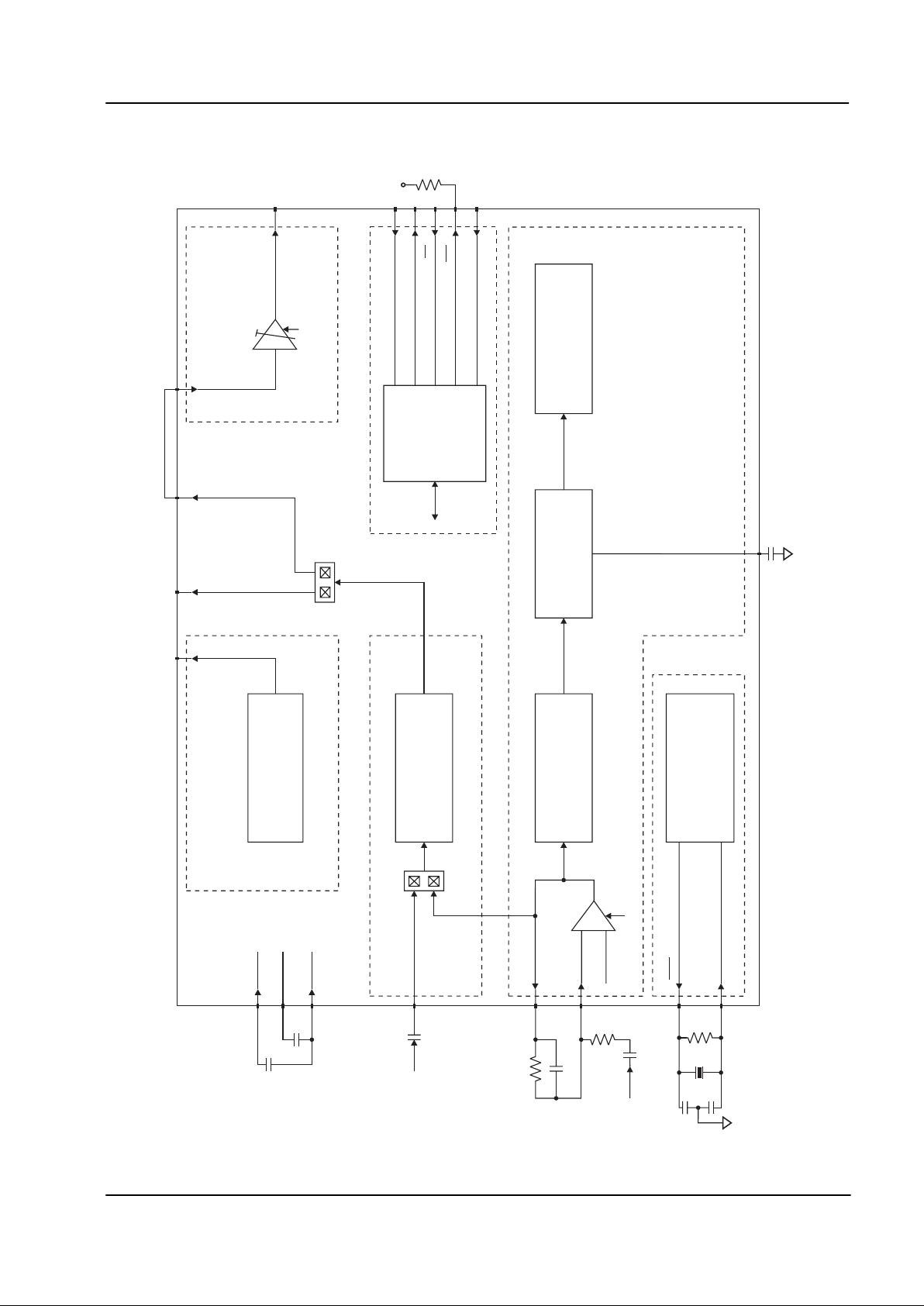
1 Block Diagram
CLOCK OSCILLATOR
AND DIVIDERS
SUB AUDIO
LPF
AUDIO
FILTER
CTCSS Tx TONE
GENERATOR
'C-BUS'
INTERFACE
AND
CONTROL
LOGIC
A to D
CONVERTER
CTCSS TONE
DECODER
V
BIASVSS
V
DD
C6
C4
TX AUDIO IN
TX AUDIO
INPUT
R1
-
+
CTCSSTx
AUDIOTx / Rx
RX AMP
Enable
V
BIAS
RXAMPOUT
RXAMPIN
C3
XT AL
XT AL/CLOCK
C5
R3
R4
C7
Input from
Demodulator
C1
C2
X1
C8
A/D CAP CTCSS Rx
TX SUB AUDIO OUT TX AUDIO OUT RX AUDIO OUT
VOLUME OUT
COMMAND DATA
REPLY DATA
CS
IRQ
SERIAL CLOCK
V
DD
R2
Enable
Volume
Control
VOLUME IN
Figure 1: Block Diagram
Page 4

Family Radio Service CTCSS Processor 4 CMX808A Preliminary Information
1999 MX-COM, Inc. www.mxcom.com tel: 800 638 5577 336 744 5050 fax: 336 744 5054 Doc. # 20480199.002
4800 Bethania Station Road, Winston-Salem, NC 27105-1201 USA All trademarks and service marks are held by their respective companies.
2 Signal List
Package /
Pin No
Signal
E3 P4 Name Type
Description
11
XTAL
output The inverted output of the on-chip oscillator.
2 2 XTAL/CLOCK input
The input to the on-chip oscillator, for external Xtal circuit or
clock.
3 3 SERIAL CLOCK input
The "C-BUS" serial clock input. This clock, produced by the
µC, is used for transfer timing of commands and data to and
from the device. See Figure 6.
4 4 COMMAND DATA input
The "C-BUS" serial data input from the µC. Data is loaded
into this device in 8-bit bytes, MSB (D7) first, and LSB (D0)
last, synchronized to the SERIAL CLOCK. See Figure 6.
5 5 REPLY DATA output
The "C-BUS" serial data output to the µC. The transmission
of REPLY DATA bytes is synchronized to the SERIAL
CLOCK under the control of the
CS
input. This 3-state
output is held at high impedance when not sending data to
the µC. See Figure 6.
66
CS
input
The "C-BUS" data loading control function: this input is
provided by the µC. Data transfer sequences are initiated,
completed or aborted by the
CS signal. See Figure 6.
77
IRQ
output
This output indicates an interrupt condition to the µC by
going to a logic "0". This is a "wire-ORable" output,
enabling the connection of up to 8 peripherals to 1 interrupt
port on the µC. This pin has a low impedance pulldown to
logic "0" when active and a high-impedance when inactive.
An external pull-up resistor is required. An interrupt is
effective if not masked out by the IRQ MASK (bit 0 in the
SUB-AUDIO CONTROL register $80).
88 NC
9NC
No internal connection. Do not make any connection to
these pins.
9 10 A/D CAP output
An internal reference voltage for the A to D converter,
decoupled to V
SS
by an external capacitor.
11 NC
No internal connection. Do not make any connection to this
pin.
10 12 V
SS
Power The negative supply rail (ground).
11 13 V
BIAS
output
A bias line for the internal circuitry, held at V
DD
/2. This pin
must be decoupled by a capacitor mounted close to the
device pins.
12 14 RX AMP IN input The inverting input to the Rx input amplifier.
13 15 RX AMP OUT output
The output of the Rx input amplifier and the input to the
audio filter section.
14 16 RX AUDIO OUT output Output of the Rx audio filter section.
17 NC
No internal connection. Do not make any connection to this
pin.
15 18 TX AUDIO IN input Input to the Tx audio filter section.
16 19 TX AUDIO OUT output Output of the Tx audio filter section.
17 20 VOLUME IN input Input to the audio volume control.
18 21 TX SUB AUDIO OUT output Output of the CTCSS tone generator.
19 22 VOLUME OUT output Output of the audio volume control.
Page 5

Family Radio Service CTCSS Processor 5 CMX808A Preliminary Information
1999 MX-COM, Inc. www.mxcom.com tel: 800 638 5577 336 744 5050 fax: 336 744 5054 Doc. # 20480199.002
4800 Bethania Station Road, Winston-Salem, NC 27105-1201 USA All trademarks and service marks are held by their respective companies.
Package /
Pin No
Signal
E3 P4 Name Type
Description
23 NC
No internal connection. Do not make any connection to this
pin.
20 24 V
DD
Power
The positive supply rail. Levels and voltages are dependent
upon this supply. This pin should be decoupled to V
SS
by a
capacitor.
Table 1: Signal List
Page 6
Family Radio Service CTCSS Processor 6 CMX808A Preliminary Information
1999 MX-COM, Inc. www.mxcom.com tel: 800 638 5577 336 744 5050 fax: 336 744 5054 Doc. # 20480199.002
4800 Bethania Station Road, Winston-Salem, NC 27105-1201 USA All trademarks and service marks are held by their respective companies.
3 External Components
V
DD
V
DD
V
SS
V
DD
V
BIAS
IRQ
XTAL
A/D CAP
SERIAL CLOCK
"C-BUS"
INTERFAC E
COMMAND DA TA
XTAL/CLOCK
RX AMP IN
R3
R4
R2
Input from
Demodulator
Tx Audio Input
CMX808AE3
TX SUB AUDIO OUT
C4
C8
C5
C3
C7
C6
REPLY DATA
CS
NC
RX AMP OUT
RX AUDIO OUT
VOLUME OUT
VOLUME IN
TX AUDIO IN
TX AUDIO OUT
1
2
3
4
5
6
8
9
10
11
12
13
14
7
20
19
18
17
16
15
XTAL
XTAL/CLOCK
C1
C2
X1
R1
Figure 2: Recommended External Components
R1 1M
: ±5% C4 0.1µF ±20%
R2 22k: ±10% C5 100pF ±20%
R3 100k: ±10% C6 0.1µF ±20%
R4 Note 1 ±10% C7 Note 1 ±20%
C1 22pF ±20% C8 0.1µF ±20%
C2 22pF ±20%
C3 0.1µF ±20% X1 Note 2 4.0MHz ±100ppm
Table 2: Recommended External Components
Recommended External Component Notes:
1. R3, R4, C5 and C7 form the gain components for the Rx Input Amplifier. R4 should be chosen as required
by the signal level, using the following formula:
R4
R3
- Gain =
C7 x R4 should be chosen so as not to compromise the low frequency performance of this product.
2. For best results, a crystal oscillator design should drive the clock inverter input with signal levels of at
least 40% of V
DD
, peak to peak. Tuning fork crystals generally cannot meet this requirement. To obtain
crystal oscillator design assistance, please consult your crystal manufacturer.
Page 7
Family Radio Service CTCSS Processor 7 CMX808A Preliminary Information
1999 MX-COM, Inc. www.mxcom.com tel: 800 638 5577 336 744 5050 fax: 336 744 5054 Doc. # 20480199.002
4800 Bethania Station Road, Winston-Salem, NC 27105-1201 USA All trademarks and service marks are held by their respective companies.
4 General Description
The CMX808A is a programmable CTCSS Processor for Family Radio Service, see Figure 1.
The receiver of the CMX808A decodes a user-programmable set of up to 7 tones with minimum software
intervention; the band-pass filter is designed to filter out the CTCSS sub-audio tones. A high-resolution tone
encoder performs accurate generation of CTCSS tones.
Each function, and the routing of signals, is flexible and may be configured or controlled by the user's
software.
4.1 Software Description
4.1.1 Address/Commands
Instructions and data are transferred, via "C-BUS", in accordance with the timing information given in Figure
6.
Instruction and data transactions to and from the CMX808A consist of an Address/Command (A/C) byte,
which may be followed by either:
(i) a further instruction or data (1 or 2 bytes) or
(ii) a status or Rx data reply (1 byte)
4.1.2 Write Only Register Description
HEX
ADDRESS/
COMMAND
REGISTER
NAME
BIT 7
(D7)
BIT 6
(D6)
BIT 5
(D5)
BIT 4
(D4)
BIT 3
(D3)
BIT 2
(D2)
BIT 1
(D1)
BIT 0
(D0)
$01
GENERAL
RESET
N/A N/A N/A N/A N/A N/A N/A N/A
CTCSS CTCSS DECODER BANDWIDTH
$80
SUB-AUDIO
CONTROL
TX
ENABLE
DECODER
ENABLE
MSB
BIT 3 BIT 2 BIT 1
LSB
BIT 0
0
CTCSS
IRQ
MASK
AUDIO ATTENUATION
$82
AUDIO
CONTROL
TX BPF
ENABLE
RX BPF
ENABLE
BPF
UN-
MUTE
MSB
BIT 4
BIT 3 BIT 2 BIT 1
LSB
BIT 0
Table 3: 8-bit Write Only Registers
HEX ADDRESS/
COMMAND
REGISTER
NAME
BIT 7
(D7)
BIT 6
(D6)
BIT 5
(D5)
BIT 4
(D4)
BIT 3
(D3)
BIT 2
(D2)
BIT 1
(D1)
BIT 0
(D0)
CTCSS TX FREQUENCY
CTCSS
TX FREQ.
(Byte 1)
CTCSS
TX
NOTONE
00
MSB
BIT 12 BIT 11 BIT 10 BIT 9 BIT 8
CTCSS TX FREQUENCY
$83
CTCSS
TX FREQ.
(Byte 2)
BIT 7 BIT 6 BIT 5 BIT 4 BIT 3 BIT 2 BIT 1
LSB
BIT 0
CTCSS TONE ADDRESS CTCSS FREQUENCY
CTCSS RX
PROGRAM
(Byte 1)
0
MSB
BIT2
BIT 1
LSB
BIT 0
MSB
BIT 11 BIT 10 BIT 9 BIT 8
CTCSS FREQUENCY
$84
CTCSS RX
PROGRAM
(Byte 2)
BIT 7 BIT6 BIT 5 BIT 4 BIT 3 BIT 2 BIT 1
LSB
BIT 0
Table 4: 16-bit Write Only Registers
4.1.2.1 GENERAL RESET (Hex address $01)
The reset command has no data attached to it. It sets the device registers to zero (all powersaved) with the
exception of Bits 2, 1 and 0 of the SUB-AUDIO STATUS register $81.
Page 8

Family Radio Service CTCSS Processor 8 CMX808A Preliminary Information
1999 MX-COM, Inc. www.mxcom.com tel: 800 638 5577 336 744 5050 fax: 336 744 5054 Doc. # 20480199.002
4800 Bethania Station Road, Winston-Salem, NC 27105-1201 USA All trademarks and service marks are held by their respective companies.
4.1.2.2 SUB-AUDIO CONTROL Register (Hex address $80)
This register is used to control the functions of the device as described below:
CTCSS TX ENABLE
and DECODER
ENABLE
(Bits 7 and 6)
These two bits enable and disable the CTCSS decoder (Rx) or transmitter (Tx)
according to Table 6.
CTCSS DECODER
BANDWIDTH
(Bits 5, 4, 3 and 2)
These four bits set the bandwidth of the CTCSS tone decoder according to Table 7.
(Bit 1)
Reserved for future use. This bit should be set to "0".
CTCSS IRQ MASK
(Bit 0)
When this bit is set to "1" it enables the interrupt.
When this bit is set to "0" the interrupt is masked.
Table 5: SUB-AUDIO CONTROL Register (Hex address $80)
Tx (Bit 7) Rx (Bit 6) Function
0 0 Tx disabled, Rx disabled
0 1 Tx disabled, Rx enabled
1 0 Tx enabled, Rx disabled
1 1 Tx enabled, Rx enabled
Table 6: CTCSS TX ENABLE and DECODER ENABLE
BANDWIDTH
Bit5Bit4Bit3Bit2Will Decode Will Not Decode
1000 ±1.1% ±2.4%
1001 ±1.3% ±2.7%
1010 ±1.6% ±2.9%
1011 ±1.8% ±3.2%
1100 ±2.0% ±3.5%
1101 ±2.2% ±3.7%
1110 ±2.5% ±4.0%
1111 ±2.7% ±4.2%
Table 7: CTCSS DECODER
Page 9

Family Radio Service CTCSS Processor 9 CMX808A Preliminary Information
1999 MX-COM, Inc. www.mxcom.com tel: 800 638 5577 336 744 5050 fax: 336 744 5054 Doc. # 20480199.002
4800 Bethania Station Road, Winston-Salem, NC 27105-1201 USA All trademarks and service marks are held by their respective companies.
4.1.2.3 AUDIO CONTROL Register (Hex address $82)
This register is used to control the functions of the device as described below:
Note: TX BPF ENABLE (Bit 7) and RX BPF ENABLE (Bit 6) should not be enabled at the same time.
TX BPF ENABLE
(Bit 7)
When this bit is "1" the audio band-pass filter is enabled and the output of the
filter is switched to TX AUDIO OUT. The output is then controlled by BPF UNMUTE. See Bit 5 below.
When this bit is “0” the audio band pass filter is disabled (powersaved) and the
output of the filter is disconnected from TX AUDIO OUT, which is then in a high
impedance state.
RX BPF ENABLE
(Bit 6)
When this bit is “1” the audio band-pass filter is enabled and the output of the
filter is switched to RX AUDIO OUT. The output is then controlled by BPF UNMUTE. See Bit 5 below.
When this bit is “0” the audio band-pass filter is disabled (powersaved) and the
output of the filter is disconnected from RX AUDIO OUT, which is then in a high
impedance state.
BPF UN-MUTE
(Bit 5)
When this bit is “1” and TX BPF ENABLE is “1” the audio band-pass filter output
is switched to the TX AUDIO OUT pin. When this bit is “0” the output of the
filter is disconnected from TX AUDIO OUT, which is then in a high impedance
state.
This control, along with TX BPF ENABLE, allows the filter to power up and
settle internally before switching the output on, when coming out of powersave.
When this bit is “1” and RX BPF ENABLE is “1” the audio band-pass filter output
is switched to the RX AUDIO OUT pin. When this bit is “0” the output of the
filter is disconnected from RX AUDIO OUT, which is then in a high impedance
state. This control, along with RX BPF ENABLE, allows the filter to power up
and settle internally before switching the output on, to avoid clicks when coming
out of powersave.
AUDIO ATTENUATION
(Bits 4, 3, 2, 1, and 0)
These five bits are used to set the attenuation of the audio volume control
according to Table 9.
Table 8: AUDIO CONTROL Register (Hex address $82)
Bits Audio
43210Attenuation
0 0 0 0 0 Off (V
BIAS
)
0 0 0 0 1 48.0dB
0 0 0 1 0 46.4dB
0 0 0 1 1 44.8dB
0 0 1 0 0 43.2dB
0 0 1 0 1 41.6dB
0 0 1 1 0 40.0dB
0 0 1 1 1 38.4dB
0 1 0 0 0 36.8dB
0 1 0 0 1 35.2dB
0 1 0 1 0 33.6dB
0 1 0 1 1 32.0dB
0 1 1 0 0 30.4dB
0 1 1 0 1 28.8dB
0 1 1 1 0 27.2dB
0 1 1 1 1 25.6dB
Page 10

Family Radio Service CTCSS Processor 10 CMX808A Preliminary Information
1999 MX-COM, Inc. www.mxcom.com tel: 800 638 5577 336 744 5050 fax: 336 744 5054 Doc. # 20480199.002
4800 Bethania Station Road, Winston-Salem, NC 27105-1201 USA All trademarks and service marks are held by their respective companies.
Bits Audio
43210Attenuation
1 0 0 0 0 24.0dB
1 0 0 0 1 22.4dB
1 0 0 1 0 20.8dB
1 0 0 1 1 19.2dB
1 0 1 0 0 17.6dB
1 0 1 0 1 16.0dB
1 0 1 1 0 14.4dB
1 0 1 1 1 12.8dB
1 1 0 0 0 11.2dB
11001 9.6dB
11010 8.0dB
11011 6.4dB
11100 4.8dB
11101 3.2dB
11110 1.6dB
11111 0dB
Table 9: AUDIO ATTENUATION
4.1.2.4 CTCSS TX FREQUENCY Register (Hex address $83)
This is a 16-bit register. Byte (1) is sent first. When the CTCSS transmitter is enabled, the bits 0 to 12 control
the frequency of the transmitted CTCSS tones according to the formula below.
A
f (Hz)
16xf (Hz)
XTAL
TONE
=
where A is the binary number programmed into the 13 bits.
When Bit 7 (in the first 8 bits) is set to "1" the tone output is set at V
BIAS
or NOTONE without regard to the
number "A" programmed. When Bit 7 is "0" the programmed tone is set on the output. Programming bits 0 to
12 to "0" sets the output to V
BIAS
. Powersave is achieved by disabling the Tx (Bit 7 in the SUB-AUDIO
CONTROL register $80).
Page 11

Family Radio Service CTCSS Processor 11 CMX808A Preliminary Information
1999 MX-COM, Inc. www.mxcom.com tel: 800 638 5577 336 744 5050 fax: 336 744 5054 Doc. # 20480199.002
4800 Bethania Station Road, Winston-Salem, NC 27105-1201 USA All trademarks and service marks are held by their respective companies.
4.1.2.5 CTCSS RX PROGRAM Register (Hex address $84)
This is a 16-bit register. Byte (1) is sent first. The two bytes are used to program the center frequencies of up
to 7 tones in the sub-audio band that will be decoded by the receiver.
Each tone is identified by its address in Bits 6, 5 and 4 of byte (1). The remaining 12 bits contain the data
representing the tone frequency according to the formula below. If a tone is not required, the 12 bits should
be set to zero.
Byte 1 Byte 2
Bit 7 Bit 6 Bit 5 Bit 4 Bit 3 Bit 2 Bit 1 Bit 0 Bit 7 Bit 6 Bit 5 Bit 4 Bit 3 Bit 2 Bit 1 Bit 0
0000
0001
0010
0011
0100
0101
0110
<----------------------- N ----------------------->
N is the binary representation of the
following decimal number (n):
×
=
XTAL
TONE
f
f948982
INTn
<----------------------- R ----------------------->
R is the nearest 6-bit binary
representation of (r), where:
8400
f4
n
f
237245
r
TONEXTAL
×
×
−=
Example: To program 100Hz when using the recommended 4.0MHz Xtal.
()
(binary) 001111R
15r
halfway)exactly if up (round 21.15r
8400
1004
23
100.4
237245
r
(binary) 010111N
2372.23INTn
100.4
100948982
INTn
6
6
=∴
=
=
×
×
−
×
=
=∴
==
×
×
=
Therefore the 12-bit code is 010111001111.
The Hex address represented by Bits 6, 5 and 4 in byte (1) is used as the code to indicate which tone has
been decoded. This code appears in Bits 2, 1 and 0 of the SUB-AUDIO STATUS register $81. The seven
programmed tones use Hex addresses $0 - $6. Address $7 should not be used.
4.1.2.6 TONE CLONING (Hex Address $9C)
This register enables and disables tone cloning as shown below:
$9C = $01 enables tone cloning
$9C = $00 disables tone cloning
The Tone Cloning Routine is shown in Figure 4.
Page 12

Family Radio Service CTCSS Processor 12 CMX808A Preliminary Information
1999 MX-COM, Inc. www.mxcom.com tel: 800 638 5577 336 744 5050 fax: 336 744 5054 Doc. # 20480199.002
4800 Bethania Station Road, Winston-Salem, NC 27105-1201 USA All trademarks and service marks are held by their respective companies.
4.1.3 Read Only Register Description
HEX
ADDRESS/COMMAND
REGISTER
NAME
BIT 7
(D7)
BIT 6
(D6)
BIT 5
(D5)
BIT 4
(D4)
BIT 3
(D3)
BIT 2
(D2)
BIT 1
(D1)
BIT 0
(D0)
CTCSS RX TONE
$81
SUB-AUDIO
STATUS
000 0
TONE
DECODE
MSB
BIT 2 BIT 1
LSB
BIT 0
Table 10: 8-bit Read Only Registers
4.1.3.1 SUB-AUDIO STATUS Register (Hex address $81)
Reading the SUB-AUDIO STATUS register clears the interrupt (
IRQ ).
This register is used to indicate the status of the device as described below:
(Bits 7, 6, 5 and 4)
Reserved for future use. These will be set to "0" but should be ignored by user's
software.
TONE DECODE
(Bit 3)
This bit indicates the status of the tone decoder. A "1" indicates a tone has been
detected (TONE DECODE) and a "0" indicates the loss of the tone (NOTONE).
TONE DECODE means that a tone has been decoded and its characteristics are
defined by the bandwidth (see SUB-AUDIO CONTROL register $80, Bits 5, 4, 3 and 2)
and the CTCSS RX TONE number (see SUB-AUDIO STATUS register $81, Bits 2, 1
and 0).
When Bit 6 in the SUB-AUDIO CONTROL register $80 is set to "0" the TONE DECODE
Bit 3 will be set to "0".
Identification of a valid tone which is not in the pre-programmed list of up to 7 tones will
cause the decoder to move to the TONE DECODE state with the RX TONE address of
"111" in Bits 2, 1 and 0; indicating a valid but unrecognized tone. Loss of tone will cause
the NOTONE timer to be started. If loss of tone continues for the duration of the timeout period, then the decoder will move to NOTONE state and the identification of preprogrammed tones will start again. The time-out period is not user adjustable.
CTCSS RX TONE
(Bits 2, 1 and 0)
These three bits hold a Hex number. Numbers $0 to $6 represent the address of the
CTCSS tone decoded according to the tones programmed in the CTCSS RX PROGRAM
register $84. The Hex number $7 indicates the presence of any tone that is not
described by CTCSS DECODER BANDWIDTH (Bits 5, 4, 3 and 2 in the SUB-AUDIO
CONTROL register $80) and CTCSS FREQUENCY (Bits 11 to 0 in the CTCSS RX
PROGRAM register $84).
Page 13

Family Radio Service CTCSS Processor 13 CMX808A Preliminary Information
1999 MX-COM, Inc. www.mxcom.com tel: 800 638 5577 336 744 5050 fax: 336 744 5054 Doc. # 20480199.002
4800 Bethania Station Road, Winston-Salem, NC 27105-1201 USA All trademarks and service marks are held by their respective companies.
4.1.3.2 Tx/Rx Enabled Set-up example
Power Up
Clear registers $01
Rx or Tx?
Tx (100Hz)
Rx
(Address 0, 100Hz, ±2.7% bandwidth,
IRQ enabled)
Program 100Hz
into address 0
$84 (1) = 00000101
$84 (2) = 11001111
Program bandwidth
to ±2.7%
Enable IRQ mask
Enable Decoder
$80 = 01111101
Enable Tx
$80 = 10000000
Program Tx
Frequency to 100Hz
$83 (1) = 00001001
$83 (2) = 11000100
Note: $8X is the Hex address/command
Figure 3: Tx/Rx Enabled
Page 14

Family Radio Service CTCSS Processor 14 CMX808A Preliminary Information
1999 MX-COM, Inc. www.mxcom.com tel: 800 638 5577 336 744 5050 fax: 336 744 5054 Doc. # 20480199.002
4800 Bethania Station Road, Winston-Salem, NC 27105-1201 USA All trademarks and service marks are held by their respective companies.
4.1.3.3 Tone Cloning Routine
The flow chart shows the tone cloning routine. The first programmed tone set ($0-$6) will decode after
typically 140ms, subsequent tone sets will decode almost instantly (i.e. the information is available at the
Reply Data Output in less than 100µs).
Note: $8X and $9C is the Hex address/command
Enable Tone
Cloning $9C=$01
Waitfor In te rrupt
Read Status
Register ($81)
Is it a
Programmed
Tone?
Tone Decoded
Yes
No
Mask Interrupt
$80=$7C
ProgramTones
($84) into
Addresses $0-$6
Read Status
Register ($81)
No
Yes
Tone Decoded
Program Bandwidth
Enable IRQ Mask
Enable Decoder
$80=$7D
Is it a
Programmed
Tone?
ProgramTones
($84) into
Addresses $0-$6
Wait 100µs
Figure 4: Tone Cloning Routine
Page 15

Family Radio Service CTCSS Processor 15 CMX808A Preliminary Information
1999 MX-COM, Inc. www.mxcom.com tel: 800 638 5577 336 744 5050 fax: 336 744 5054 Doc. # 20480199.002
4800 Bethania Station Road, Winston-Salem, NC 27105-1201 USA All trademarks and service marks are held by their respective companies.
5 Application Notes
5.1 General
The CMX808A is intended for use in radio systems where subaudio tone signaling is required for functions
such as Family Radio Service (FRS) Hand-helds, Amateur Radio Equipment, General Mobile Radio Service
(GMRS) and Short Range Business Radio.
The facility to decode any one of 7 programmed tones (or one-of-any if tone sets are dynamically
reconfigured) allows designers to offer attractive end features to:
•
Simultaneously support multiple calling tone codes e.g. children, parents and family with unique paging
and/or visual alerts used to identify each calling party or group.
•
Effectively scan and 'learn' received tones to make Rx tone configuration easy and nearly automatic.
Configurable decoder bandwidths provide the flexibility to optimize performance under different operating
conditions such as when congestion or long distances alter signal quality.
5.2 Transmitter
The transmitter is enabled with Bit 7 in the SUB-AUDIO CONTROL register $80.
The Tx frequency is set using bits 0 to 12 in the CTCSS TX FREQUENCY register $83, using the formula
below:
)Hz(f16
)Hz(f
A
TONE
XTAL
×
=
Where A is the binary number programmed into the 13 bits.
When Bit 7 (in the first 8 bits) is set to "1" the tone output is set at V
BIAS
or NOTONE without regard to the
number "A" programmed. When Bit 7 is "0" the programmed tone is set on the output. Programming bits 0 to
12 to "0" sets the output to V
BIAS
. Powersave is also achieved by disabling the Tx (Bit 7 in the SUB-AUDIO
CONTROL register $80).
Page 16

Family Radio Service CTCSS Processor 16 CMX808A Preliminary Information
1999 MX-COM, Inc. www.mxcom.com tel: 800 638 5577 336 744 5050 fax: 336 744 5054 Doc. # 20480199.002
4800 Bethania Station Road, Winston-Salem, NC 27105-1201 USA All trademarks and service marks are held by their respective companies.
5.3 Tx Tone Table
The following table lists the commonly used CTCSS tones and the corresponding values for programming the
CTCSS TX FREQUENCY register $83.
STANDARD TONES
Freq. Byte 1 Byte 2 Freq. Byte 1 Byte 2 Freq. Byte 1 Byte 2
(Hz) (Hex) (Hex) (Hz) (Hex) (Hex) (Hz) (Hex) (Hex)
67.0 0E 93 103.5 09 6F 162.2 06 05
69.3 0E 18 107.2 09 1C 167.9 05 D1
71.9 0D 95 110.9 08 CE 173.8 05 9E
74.4 0D 20 114.8 08 82 179.9 05 6E
77.0 0C AF 118.8 08 38 186.2 05 3F
79.7 0C 41 123.0 07 F1 192.8 05 11
82.5 0B D6 127.3 07 AC 203.5 04 CD
85.4 0B 6F 131.8 07 69 210.7 04 A3
88.5 0B 09 136.5 07 28 218.1 04 7A
91.5 0A AC 141.3 06 E9 225.7 04 54
94.8 0A 4D 146.2 06 AE 233.6 04 2E
97.4 0A 07 151.4 06 73 241.8 04 0A
100.0 09 C4 156.7 06 3B 250.3 03 E7
NON-STANDARD TONES
Freq. Byte 1 Byte 2 Freq. Byte 1 Byte 2 Freq. Byte 1 Byte 2
(Hz) (Hex) (Hex) (Hz) (Hex) (Hex) (Hz) (Hex) (Hex)
62.5 0F A0 183.5 05 52 199.5 04 E5
64.7 0F 18 189.9 05 24 206.5 04 BB
159.8 06 1C 196.6 04 F8 229.1 04 43
5.4 Receiver (Decode)
The CTCSS Receiver (Decoder) should first be set up according to the desired characteristics. This entails
setting the CTCSS DECODER BANDWIDTH in the SUB-AUDIO CONTROL register $80, also programming
the center frequencies of the desired tones in the CTCSS RX PROGRAM register $84. (It can hold up to 7
different tones). Any tone can be in any location. During operation when the device is receiving, the tones
are scanned in the sequence of their location, i.e. $0 first and $6 last and once a tone is detected the
remaining tones are not checked. Therefore, if two tones are close enough in frequency for their bandwidths
to overlap then the one in the lowest location will be detected.
The CTCSS IRQ MASK in the SUB-AUDIO CONTROL register $80 should also be set as required.
The CTCSS DECODER ENABLE in the SUB-AUDIO CONTROL register $80 should then be set to "1".
The TONE CLONING register $9C should be set as required.
When the receiver detects a change in its present state an interrupt will be generated. The change that
occurred can be read from Bit 3 of the SUB-AUDIO STATUS register $81 and if a tone is indicated by these
bits then the number of that tone can be read from Bits 2, 1 and 0 of the same register. The interrupt is
cleared by reading the SUB-AUDIO STATUS register.
Page 17

Family Radio Service CTCSS Processor 17 CMX808A Preliminary Information
1999 MX-COM, Inc. www.mxcom.com tel: 800 638 5577 336 744 5050 fax: 336 744 5054 Doc. # 20480199.002
4800 Bethania Station Road, Winston-Salem, NC 27105-1201 USA All trademarks and service marks are held by their respective companies.
5.5 Rx Tone Table
The following table lists the commonly used CTCSS tones together with the values for programming the
CTCSS RX PROGRAM register $84 for tone address 0. (Tone addresses 1 to 6 are also available.) Other
tones within the supported tone range can also be configured as described in Section 4.1.2.5.
NOTE: The most significant nibble (four bits) of Byte 1 determines the tone register address being configured
and is independent of the configured tone frequency. For example, this nibble (left hex character of Byte 1) is
set to $0 (hex), corresponding to tone address 0, for all entries in the table below. As another example the
same tone table for tone address 5 would require this nibble to be set to $5 (hex) for all values in the table
e.g. 67.0Hz would be $53 (Byte 1) $DC (Byte 2).
STANDARD TONES
Freq. Byte 1 Byte 2 Freq. Byte 1 Byte 2 Freq. Byte 1 Byte 2
(Hz) (Hex) (Hex) (Hz) (Hex) (Hex) (Hz) (Hex) (Hex)
67.0 03 DC 103.5 06 0B 162.2 09 86
69.3 04 0D 107.2 06 48 167.9 09 CA
71.9 04 42 110.9 06 86 173.8 0A 43
74.4 04 52 114.8 06 C4 179.9 0A 88
77.0 04 87 118.8 07 03 186.2 0B 02
79.7 04 98 123.0 07 43 192.8 0B 48
82.5 04 CF 127.3 07 83 203.5 0C 03
85.4 05 06 131.8 07 C4 210.7 0C 4A
88.5 05 18 136.5 08 06 218.1 0C C7
91.5 05 50 141.3 08 48 225.7 0D 45
94.8 05 8B 146.2 08 8A 233.6 0D C4
97.4 05 C2 151.4 08 CD 241.8 0E 43
100.0 05 CF 156.7 09 42 250.3 0E C3
NON-STANDARD TONES
Freq. Byte 1 Byte 2 Freq. Byte 1 Byte 2 Freq. Byte 1 Byte 2
(Hz) (Hex) (Hex) (Hz) (Hex) (Hex) (Hz) (Hex) (Hex)
62.5 03 9C 183.5 0A C6 199.5 0B C3
64.7 03 CB 189.9 0B 41 206.5 0C 0A
159.8 09 4C 196.6 0B 87 229.1 0D 83
Page 18

Family Radio Service CTCSS Processor 18 CMX808A Preliminary Information
1999 MX-COM, Inc. www.mxcom.com tel: 800 638 5577 336 744 5050 fax: 336 744 5054 Doc. # 20480199.002
4800 Bethania Station Road, Winston-Salem, NC 27105-1201 USA All trademarks and service marks are held by their respective companies.
6 Performance Specification
6.1 Electrical Performance
6.1.1 Absolute Maximum Ratings
Exceeding these maximum ratings can result in damage to the device.
Min. Max. Units
Supply (VDD - VSS) -0.3 7.0 V
Voltage on any pin to V
SS
-0.3 V
DD
+ 0.3 V
Current into or out of:
V
DD
-30 +30 mA
V
SS
-30 +30 mA
Any other pin -20 +20 mA
E3 Package
Total Allowable Power Dissipation at T
AMB
= 25°C 300 mW
Derating above 25°C 5 mW/°C above 25°C
Storage Temperature -55 +125 °C
Operating Temperature -40 +85 °C
P4 Package
Total Allowable Power Dissipation at T
AMB
= 25°C 800 mW
Derating above 25°C 13 mW/°C above 25°C
Storage Temperature -55 +125 °C
Operating Temperature -40 +85 °C
6.1.2 Operating Limits
Correct operation of the device outside these limits is not implied.
Notes Min. Max. Units
Supply (VDD - VSS)3.05.5V
Operating Temperature -40 85 °C
Xtal Frequency 3.9996 4.0004 MHz
Page 19

Family Radio Service CTCSS Processor 19 CMX808A Preliminary Information
1999 MX-COM, Inc. www.mxcom.com tel: 800 638 5577 336 744 5050 fax: 336 744 5054 Doc. # 20480199.002
4800 Bethania Station Road, Winston-Salem, NC 27105-1201 USA All trademarks and service marks are held by their respective companies.
6.1.3 Operating Characteristics
For the following conditions unless otherwise specified:
Xtal Frequency = 4.0MHz, Audio Level 0dB ref. = 308mV
RMS
at 1kHz
V
DD
= 3.0V to 5.0V, T
AMB
= -40°C to +85°C,
Composite Signal = 308mV
RMS
at 1kHz + 75mV
RMS
Noise + 31mV
RMS
Sub-Audio Signal
Noise Bandwidth = 5kHz Band Limited Gaussian
Notes Min. Typ. Max. Units
DC Parameters
At V
DD
= 3.0V
IDD (powersaved) 2 0.2 0.3 mA
IDD (Encoder or Decoder only Operating) 2 1.3 2.0 mA
At V
DD
= 5.0V
IDD (powersaved) 2 0.5 0.8 mA
IDD (Encoder or Decoder only Operating) 2 3.2 4.8 mA
"C-BUS" Interface
Input Logic "1" 70% V
DD
Input Logic "0" 30% V
DD
Input Leakage Current (Logic "1" or "0") -1.0 1.0 µA
Input Capacitance 7.5 pF
Output Logic "1" (IOH = 120µA) 90% V
DD
Output Logic "0" (IOL = 360µA) 10% V
DD
"Off" State Leakage Current (V
OUT
= VDD) 3 10.0 µA
AC Parameters
CTCSS Decoder
Sensitivity (Pure CTCSS Tone) 5 -26.0 dB
Response Time (Composite Signal) 140 ms
De-Response Time (Composite Signal) 145 ms
Frequency Range 60.0 251 Hz
CTCSS Encoder
Frequency Range 60.0 251 Hz
Tone Frequency Resolution 0.3 %
Tone Amplitude Tolerance 1 -1.0 0 1.0 dB
Total Harmonic Distortion 3.0 %
Audio Band-Pass Filter
Passband 6 350 3000 Hz
Passband Gain (at 1.0kHz) 6 - 0 dB
Passband Ripple (with respect to gain at 1.0kHz) 6 -2.0 +0.5 dB
Stopband Attenuation 6 30.0 dB
Residual Hum and Noise -50.0 dBp
Alias Frequency 62.5 kHz
Audio Attenuator
Nominal Adjustment Range 0 48 dB
Attenuation Accuracy -1.5 1.5 dB
Step Size 1.6 dB
Page 20

Family Radio Service CTCSS Processor 20 CMX808A Preliminary Information
1999 MX-COM, Inc. www.mxcom.com tel: 800 638 5577 336 744 5050 fax: 336 744 5054 Doc. # 20480199.002
4800 Bethania Station Road, Winston-Salem, NC 27105-1201 USA All trademarks and service marks are held by their respective companies.
Notes Min. Typ. Max. Units
Output Impedances
TX SUB-AUDIO OUT (Enabled) 2.0
k
Ω
TX/RX AUDIO OUT (Enabled) 600
Ω
TX/RX AUDIO OUT (Disabled) 500
k
Ω
VOLUME OUT (Enabled) 7 600
Ω
Rx Amplifier
Open Loop Gain (input = 1mV at 100Hz) 70.0 dB
Unity Gain Bandwidth 5.0 MHz
Input Impedance (at 100Hz) 10.0
M
Ω
Output Impedance (Open Loop) 6.0
k
Ω
Xtal/Clock Input
Pulse Width ('High' or 'Low') 4 40.0 ns
Input Impedance (at 100Hz) 10.0
M
Ω
Gain (input = 1mV
RMS
at 100Hz) 20.0 dB
Notes:
1. At V
DD
= 5.0V only. Signal levels or currents are proportional to VDD.
2. Not including any current drawn from the device pins by external circuitry.
3.
IRQ pin.
4. Timing for an external input to the XTAL/CLOCK pin.
5. With input gain components set as recommended in Figure 2.
6. See filter response (Figure 5).
7. Small signal impedance V
DD
= 5.0V and T
AMB
= 25°C. A minimum load resistance of 6kΩ is suggested.
-50
-45
-40
-35
-30
-25
-20
-15
-10
-5
0
5
10 100 1,000 10,000 100,000
Frequency (Hz)
Gain (dB)
350Hz
250Hz
3kHz
Figure 5: Audio Band-Pass Filter Frequency Response
Page 21

Family Radio Service CTCSS Processor 21 CMX808A Preliminary Information
1999 MX-COM, Inc. www.mxcom.com tel: 800 638 5577 336 744 5050 fax: 336 744 5054 Doc. # 20480199.002
4800 Bethania Station Road, Winston-Salem, NC 27105-1201 USA All trademarks and service marks are held by their respective companies.
6.1.4 Timing Diagrams
For the following conditions unless otherwise specified:
Xtal Frequency = 4.0MHz, V
DD
= 3.0V to 5.0V, T
AMB
= -40°C to 85°C.
Parameter Notes Min. Typ. Max. Units
t
CSE
"CS-Enable to Clock-High" 2.0 µs
t
CSH
Last "Clock-High to CS-High" 4.0 µs
t
HIZ
"CS-High to Reply Output 3-state" 2.0 µs
t
CSOFF
"CS-High" Time between transactions 2.0 µs
t
NXT
"Inter-Byte" Time 4.0 µs
t
CK
"Clock-Cycle" Time 2.0 µs
Notes:
1. Depending on the command, 1 or 2 bytes of COMMAND DATA are transmitted to the peripheral MSB
(Bit 7) first, LSB (Bit 0) last. REPLY DATA is read from the peripheral MSB (Bit 7) first, LSB (Bit 0) last.
2. Data is clocked into and out of the peripheral on the rising SERIAL CLOCK edge.
3. Loaded commands are acted upon at the end of each command.
4. To allow for differing µC serial interface formats "C-BUS" compatible ICs are able to work with either
polarity SERIAL CLOCK pulses.
7
6
5
4321
0
7
6
5
4321
0
7
6
5
4321
0
0
12
3
4
5
6
77
6
5
4321
0
MSB
LSB
FIRST REPL Y DATA BYTE LAST REPLY DATA BYTE
Logic level is not important
REPLY DA TA
MSB LSB
ADDRESS/COMMAND BYTE
COMMAND DATA
SERIAL CLOCK
t
CSE
FIRST DATA BYTE LAST DATA BYTE
t
HIZ
t
CK
t
NXT
t
NXT
t
CSH
t
CSOFF
CS
Figure 6: "C-BUS" Timing
Page 22

Family Radio Service CTCSS Processor 22 CMX808A Preliminary Information
1999 MX-COM, Inc. www.mxcom.com tel: 800 638 5577 336 744 5050 fax: 336 744 5054 Doc. # 20480199.002
4800 Bethania Station Road, Winston-Salem, NC 27105-1201 USA All trademarks and service marks are held by their respective companies.
6.2 Packaging
Figure 7: 20-pin TSSOP Mechanical Outline:
Order as part no. CMX808AE3
NOTE: All dimensions in inches (mm.)
Angles are in degrees
PackageTolerances
A
B
C
E
E1
H
TYP. MAX.MIN.DIM.
J
J1
P
Y
T
K
L
0.220 (5.59)
0.555 (14.04)
0.670 (17.02)
7°
0.160 (4.05)
1.270 (32.26)
0.151 (3.84)
0.100 (2.54)
0.121 (3.07)
0.600 (15.24)
0.590 (14.99) 0.625 (15.88)
0.015 (0.38) 0.045 (1.14)
0.008 (0.20) 0.015 (0.38)
0.015 (0.38) 0.023 (0.58)
0.040 (1.02) 0.065 (1.65)
0.066 (1.67) 0.074 (1.88)
1.200 (30.48)
0.500 (12.70)
H
K
L
J1J1
JJ
PP
CC
BB
AA
PIN1PIN1
TT
EE
E1E1
Y
Figure 8: 24-pin PDIP Mechanical Outline:
Order as part no. CMX808AP4
 Loading...