

Page 1
CMX673
Call Progress
Tone Detector
2001 Consumer Microcircuits Limited
D/673/5 June 2001 Provisional Issue
Features Applications
• Worldwide Tone Compatibility • Worldwide Payphone Systems
• Single and Dual Tones Detected • Telephone Redialling Systems
• Wide Dynamic Signal Range • Dialling Modems
• Fast Response Time • Banking and Billing Systems
• Low Power Operation 500µA at 3.0V • Telecom Test Equipment
• 3.58MHz Xtal/Clock Oscillator • Telecom Security Systems
1.1 Brief Description
The CMX673 is a general purpose call progress tone detector for use in Public Switched Telephone
System (PSTN) applications. Call progress detection allows equipment which dials into the PSTN
network to monitor the progress of the resulting call. Ringing, Busy, Not available and Answer states can
be determined. The CMX673 uses advanced digital signal processing techniques to detect tones in the
frequency band 315Hz to 650Hz. The use of DSP techniques allows the CMX673 to distinguish between
valid call progress tone signals and line noise or voice, low false detection rates result. This is in contrast
to other call progress detection devices which are based on simple filtering techniques. The detection
timing of the CMX673 allows it to operate with almost any call progress system. In particular the ‘stuttered
dial tone’ of voice mail messaging systems is supported. The use of digital processing and small
geometry CMOS design techniques allows the CMX673 to offer a complete call progress detector which
analyses both frequency and amplitude in a single 8 pin package. This, coupled with industry leading
performance and substantially lower power supply requirements than comparable devices, demonstrates
CML’s unique capability in this area. A single 3.58MHz crystal ensures accurate and repeatable
performance. With supply requirements between 2.7V and 5.5V the CMX673 can be easily integrated
into a wide range of telecom equipments. The CMX673 is pin to pin compatible with the M980 and TSC
75T980 and SSI980. It is available in DIP, TSSOP and SOIC packages. The CMX673 integrated circuit
coupled with cadence measurement of the signals detected can identify virtually all call progress tones
used worldwide.
Page 2

2001 Consumer Microcircuits Limited 2 D/673/5
CONTENTS
Section Page
1.0 Features and Applications............................................................. 1
1.1 Brief Description.................................................................................2
1.2 Block Diagram ...................................................................................... 3
1.3 Signal List.............................................................................................. 4
1.4 External Components....................................................................... 5
1.5 General Description........................................................................... 6
1.5.1 Overall Function Description..................................................... 6
1.5.1 Software Description.................................................................. 6
1.5.2 Glossary........................................................................................ 6
1.5.3 Block Diagram Description........................................................7
1.5.4 Decode Output Truth Table ....................................................... 7
1.6 Application Notes............................................................................... 8
1.6.1 General.......................................................................................... 8
1.7 Performance Specification.............................................................9
1.7.1 Electrical Performance............................................................... 9
1.7.2 Packaging...................................................................................12
Page 3
2001 Consumer Microcircuits Limited 3 D/673/5
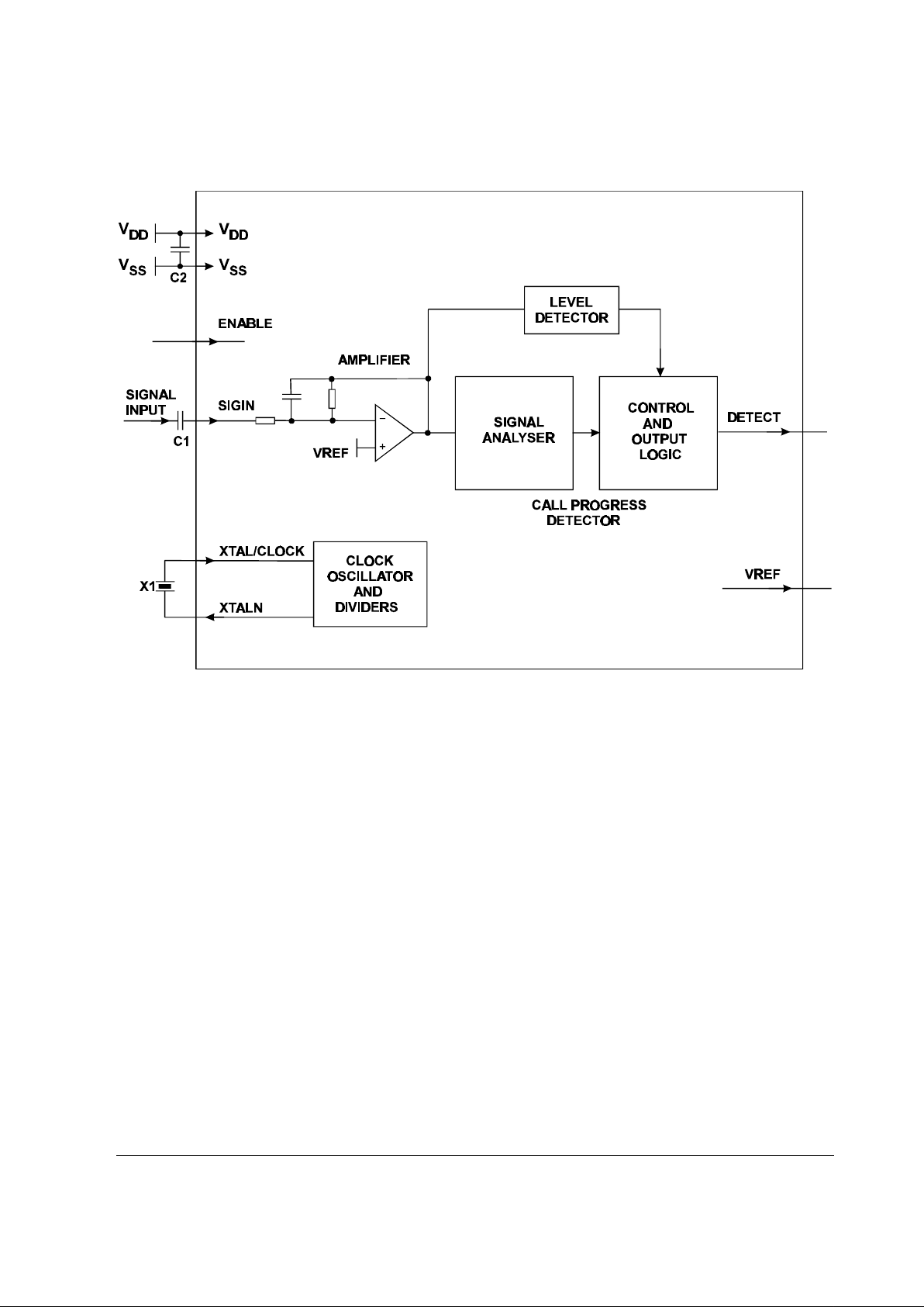
1.2 Block Diagram
Figure 1 Block Diagram
Page 4

2001 Consumer Microcircuits Limited 4 D/673/5
1.3 Signal List
Package
D4 E3 P1
Signal Description
Pin
No.
Pin
No.
Pin
No.
Name Type
2 3 1 XTAL/CLOCK I/P The input to the on-chip oscillator and external
clock input. Components are on chip.
4 5 2 XTALN O/P The inverted output of the on-chip oscillator.
5 7 3 ENABLE I/P A logic ‘1’ applied to this input enables the
DETECT output. A logic ‘0’ will reset
DETECT output to a logic ‘0’.
7 8 4 DETECT O/P When a call progress signal is detected, this
output goes to a logic ‘1’.
10 13 5 SIGIN I/P Signal input. Signals to this pin should be ac
coupled. The dc bias of this pin is set
internally.
12 15 6 VSS Power The negative supply rail (ground).
14 17 7 VREF O/P Internally generated reference voltage, held at
½VDD.
15 18 8 VDD Power The positive supply rail. This pin should be
decoupled to V
SS
by a capacitor.
1, 3, 6,
8, 9,
11, 13,
16
1, 2, 4,
6, 9,
10, 11,
12, 14,
16, 19,
20
NC Internal Connection. Do not make any
connection to these pins.
Notes: I/P = Input
O/P = Output
BI = Bidirectional
Page 5

2001 Consumer Microcircuits Limited 5 D/673/5
1.4 External Components
Typical Values:
C1 0.1µF ± 20%
C2 1µF ± 20%
X1 3.579545MHz (refer to Section 1.7.1)
Note: C1 is not required if the input is referenced to VREF.
Figure 2 Recommended External Components
Page 6

2001 Consumer Microcircuits Limited 6 D/673/5
1.5 General Description
1.5.1 Overall Function Description
The CMX673 Call Progress Tone Detector uses different tone detection methods from those
commonly found with other products.
Many traditional devices from other suppliers use a bandpass filter followed by an energy
detector. The filter is usually designed to pass input signals with a frequency between about
300Hz and 700Hz, and the amplitudes of signals in this range are then checked against a level
threshold. Any signal of acceptable level in this frequency band is classed as a Call Progress
tone, including signals due to speech and noise. False outputs caused by speech are a common
feature with these products, and background noise may lead to a stuck “detect” output.
The CMX673, by contrast, uses a stochastic signal processing technique based on analysis in
both the frequency and time domains, with signal amplitude forming part of the decision process.
This analysis includes checks on whether the signal has a “profile” which matches international
standards for Call Progress tone, or a profile more likely to match that of speech, noise or no
signal.
The following Glossary, and the Decode Truth Table in Section 1.5.4 provide a simple
explanation of the decoding functions and features offered by the CMX673.
1.5.2 Glossary
Call Progress Tones: The single and dual frequency tones in the range 350Hz to 620Hz
specified widely for call progress signalling.
Call Progress Band: The nominal range 315Hz to 650Hz within which the CMX673 will detect
Call Progress tones. The detection algorithm requires that the tones have the characteristics
typical of Call Progress Tones.
No Signal: The absence of an input signal or
A signal below 250Hz or
A signal between 750Hz and 10kHz.
Note that signals above 10kHz should be at a level below -38dBm so as to avoid
aliasing.
Nominal: Subject to dynamic tolerances within the signal analysis process. Absolute values are
not material or adverse to performance.
Page 7

2001 Consumer Microcircuits Limited 7 D/673/5
1.5.3 Block Diagram Description
Amplifier
The input signal is amplified by a self-biased inverting amplifier. The dc bias of this input is
internally set at ½V
DD.
Signal Analyser
The frequency range, quality and consistency of the input signal is analysed by this functional
block. To be classified as a call progress signal the input signal frequencies should lie between
315Hz and 650Hz. The signal to noise ratio must be 16dB or greater. The signal must be
consistent over a period of about 80ms. These decode criteria are continuously monitored and
the assessment is updated every 6ms; reference Figure 4.
Control Logic
This block categorises the nature of the signal into two decoded output states and controls the
output pin. See the Decode Output Truth Table in Section 1.5.4.
Level Detector
The level detector operates by measuring the level of the amplified input signal and comparing it
with a preset threshold. The level detector output goes to the Control and Output Logic block.
The data output is gated with the level detector’s output. The data output is valid only if the level
detector output is true.
Xtal/Clock Oscillator
If the on-chip Xtal oscillator is to be used, then external component X1 is required. If an external
clock source is to be used, then it should be connected to the XTAL/CLOCK input pin and the
XTALN pin should be left unconnected.
1.5.4 Decode Output Truth Table
“DETECT” CONDITIONS
0 No Signal
1 Call Progress Band:
Will detect 350+440, 400+450, 440+480
400, 425,440, 450, 480+620, 600 and 620Hz tones
Note that DETECT responds to the whole range of call progress tones from 315Hz to 650Hz.
Table 1 Decode Output Truth Table
Page 8

2001 Consumer Microcircuits Limited 8 D/673/5
1.6 Application Notes
1.6.1 General
On power-up, it will take 80ms to initialise the internal state, this delay should be accounted for
before the DETECT output is valid.
C3
C4
R2
R3
R5
R1
Phon
e
Line
To/FromµC
R4
C2
X1
XTALN
XTAL/CLOCK
8
7
2
3
4
5
6
DETECT
CMX673P1
ENABLE
SIGIN
VREF
1
+
_
Figure 3 A typical Telephone Line Circuit Application
R1 470kΩ R5 160kΩ
R2 470kΩ
C3 0.01µF 250V
R3 240kΩ
C4 0.01µF 250V
R4 470kΩ
Note: 1. Resistors ±1%, Capacitors ±20% unless otherwise stated.
2. A low offset opamp is needed.
An alternative set of component values can be used:
R1 499kΩ R5 49.9kΩ
R2 499kΩ
C3 0.001µF 300V
R3 54.9kΩ
C4 0.001µF 300V
R4 499kΩ
Note: 3. Resistors ±1%, Capacitors ±2% unless otherwise stated.
4. A higher value of C3 and C4 will reduce the level sensitivity tolerance at around -38dBm.
Page 9

2001 Consumer Microcircuits Limited 9 D/673/5
1.7 Performance Specification
1.7.1 Electrical Performance
Absolute Maximum Ratings
Exceeding these maximum ratings can result in damage to the device.
Min. Max. Units
Supply (VDD - VSS) -0.3 7.0 V
Voltage on any pin to VSS -0.3 V
DD
+ 0.3 V
Current into or out of VDD and V
SS
pins -30 +30 mA
Current into or out of any other pin -20 +20 mA
P1 Package Min. Max. Units
Total Allowable Power Dissipation at Tamb = 25°C 800 mW
... Derating 13.0 mW/°C
Storage Temperature -55 +125 °C
Operating Temperature -40 +85 °C
E3 Package Min. Max. Units
Total Allowable Power Dissipation at Tamb = 25°C 300 mW
... Derating 5.0 mW/°C
Storage Temperature -55 +125 °C
Operating Temperature -40 +85 °C
D4 Package Min. Max. Units
Total Allowable Power Dissipation at Tamb = 25°C 800 mW
... Derating 13.0 mW/°C
Storage Temperature -55 +125 °C
Operating Temperature -40 +85 °C
Operating Limits
Correct operation of the device outside these limits is not implied.
Notes Min. Max. Units
Supply (VDD - VSS) 2.7 5.5 V
Xtal Frequency 3.57 3.59 MHz
Page 10

2001 Consumer Microcircuits Limited 10 D/673/5
Operating Characteristics
For the following conditions unless otherwise specified:
Xtal Frequency = 3.579545MHz, S/N = 16dB, Noise Bandwidth = 5kHz,
V
DD
= 3.0V to 5.0V, Tamb = -40°C to +85°C. 0dB = 775mVrms.
Notes Min. Typ. Max. Units
DC Parameters
IDD (ENABLE = ‘1’) (VDD = 5.0V) 1 1.0 1.5 mA
IDD (ENABLE = ‘1’) (VDD = 3.0V) 1 0.5 1.0 mA
AC Parameters
SIGIN pin
Input Impedance 2 0.1
MΩ
Minimum Input Signal Level -38.0 dB
Input Signal Dynamic Range 40.0 dB
Signal to Noise Ratio 16.0
Xtal/Clock Input
‘High’ Pulse Width 3 100 ns
‘Low’ Pulse Width 3 100 ns
Gain (I/P = 1mVrms at 100Hz) 20.0 dB
Level Detector
Must Detect Signal Level 4 -38.0 dB
Must Not Detect Signal Level 4 -50.0 dB
Call Progress Band 7
Must Detect Range 315 650 Hz
Must Not Detect Range 750 250 Hz
Logic Interface
Input Logic “1” Level 5 80% VDD
Input logic "0" level 5 20% VDD
Input leakage current (Vin = 0 to VDD) 5 -5.0 +5.0 µA
Input Capacitance 5 10.0 pF
Output logic "1" level (lOH = 120µA) 6 90% VDD
Output logic "0" level (l
OL
= 360µA) 6 10% VDD
Notes: 1. Not including any current drawn from the detector pins by external circuitry.
2. Small signal impedance over the frequency range 100Hz to 2000Hz and at V
DD
= 5.0V.
3. Timing for an external input to the XTAL/CLOCK pin.
4. Input signal level at V
DD
= 5.0V, scale signal for different VDD.
5. ENABLE pin.
6. DETECT pin.
7. Nominal values which are subject to dynamic tolerances within the signal analysis process,
as a result of using stochastic signal processing techniques.
Page 11

2001 Consumer Microcircuits Limited 11 D/673/5
Electrical Performance (continued)
Figure 4 µµ C Parallel Interface Timings
For the following conditions unless otherwise specified:
Xtal Frequency = 3.579545MHz, V
DD
= 3.0V to 5.0V, Tamb = -40°C to +85°C, S/N = 20dB.
Notes Min. Typ. Max. Units
Signal Timings (ref. Figures 3, 4 and 5)
tl Burst Length Ignored 40.0 ms
tL Burst Length Detected 80.0 ms
tGI Call Progress Tone Gap Length
Ignored
8 20.0 ms
tGD
Call Progress Tone Gap Length
Detected
8 40.0 ms
tRP Call Progress Tone Response Time 9 80.0 ms
t
DRP
Call Progress Tone De-Response
Time
9 80.0 ms
Notes: 8. Only applies to bursts of the same frequency.
9. Measured with 350+440Hz tone pair.
Page 12

2001 Consumer Microcircuits Limited 12 D/673/5
1.7.2 Packaging
Figure 5 P1 Mechanical Outline: Order as part no. CMX673P1
Figure 6 E3 Mechanical Outline: Order as part no. CMX673E3
Page 13

Call Progress Tone Detector CMX673
Handling precautions: This product includes input protection, however, precautions should be taken to prevent device damage from
electro-static discharge. CML does not assume any responsibility for the use of any circuitry described. No IPR or circuit patent
licences are implied. CML reserves the right at any time without notice to change the said circuitry and this product specification.
CML has a policy of testing every product shipped using calibrated test equipment to ensure compliance with this product
specification. Specific testing of all circuit parameters is not necessarily performed.
Oval Park - LANGFORD
MALDON - ESSEX
CM9 6WG - ENGLAND
Telephone: +44 (0)1621 875500
Telefax: +44 (0)1621 875600
e-mail: sales@cmlmicro.co.uk
http://www.cmlmicro.co.uk
Figure 7 D4 Mechanical Outline: Order as part no. CMX673D4
 Loading...