

Page 1
DATA BULLETIN
CMX654
¤1998 MX-COM, Inc. www.mxcom.com Tel: 800 638 5577 336 744 5050 Fax: 336 744 5054 Doc. # 20480186.001
4800 Bethania Station Road, Winston-Salem, NC 27105-1201 USA All Trademarks and Service marks are held by their respective companies.
V.23 TRANSMIT
MODULATOR
PRELIMINARY INFORMATION
Features Applications
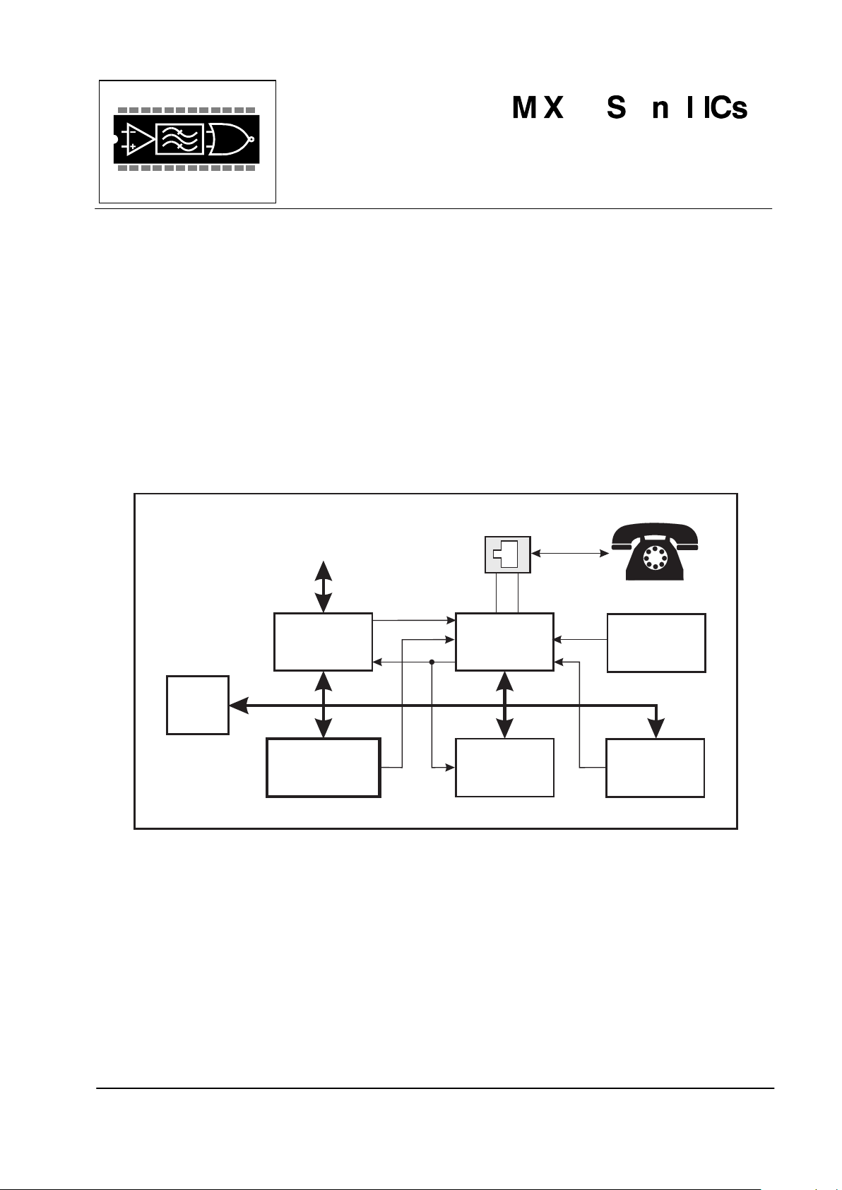
x 1200bits/sec, V.23 Transmit Modulator
x 3.0V to 5.5V Supply:
1mA typical at 3V
x Zero Power Mode:
1µA typical
x 1200bits/sec Tx Data Retiming
x 3.58MHz Xtal/Clock Rate
x Meets ITU and ETSI Specifications
x Caller ID generation for:
ISDN Terminal Adapters
Wireless Local Loop System
ISDN PABX Applications
Pair-Gain Systems
Public Switched Telephone
Networks
Trunk Exchanges
Digital
Line Circuit
CODEC
µC
V23T ransmit
Modulator
SLIC
DTMF
DECODER
RINGING
GENERATOR
DC-to-DC
CONVERTER
POTS
CMX654
The CMX654 is a low power integrated circuit, designed for the transmission of asynchronous 1200bits/sec
data in accordance with ITU, V.23 and ETSI specifications.
The device incorporates an optional Tx data retiming function. This device may be operated so that only the
mark or space tone is produced.
The CMX654 may be used in a wide range of telephone telemetry systems. With a low voltage requirement of
3.0V it is suitable for both portable terminal and line powered applications. A very low current 'sleep' mode
(1PA typ.) and an operating current of 1mA typ. makes the CMX654 ideal for line powered applications.
This device requires a standard 3.58MHz Xtal/Clock rate and operates from a 3.0 to 5.5V supply. Available
packages are: 16-pin SOIC (CMX654D4) and 16-pin PDIP (CMX654P3). Additional package styles may be
available to meet specific design requirements.
Page 2

V.23 Transmit Modulator 2 CMX654 PRELIMINARY INFORMATION
¤1998 MX-COM, Inc. www.mxcom.com Tel: 800 638 5577 336 744 5050 Fax: 336 744 5054 Doc. # 20480186.001
4800 Bethania Station Road, Winston-Salem, NC 27105-1201 USA All Trademarks and Service marks are held by their respective companies.
CONTENTS
Section Page
1 Block Diagram................................................................................................................3
2 Signal List.......................................................................................................................4
3 External Components....................................................................................................5
4 General Description.......................................................................................................6
4.1 Xtal Oscillator and Clock Dividers ....................................................................................... 6
4.2 Mode Control Logic ............................................................................................................. 6
4.3 FSK Modulator and Transmit Filter...................................................................................... 6
4.4 Tx Data Retiming................................................................................................................. 7
5 Application Notes ..........................................................................................................8
5.1 Line Interface....................................................................................................................... 8
6 Performance Specification............................................................................................9
6.1 Electrical Performance ........................................................................................................ 9
6.1.1 Absolute Maximum Ratings....................................................................................................9
6.1.2 Operating Limits.....................................................................................................................9
6.1.3 Operating Characteristics.....................................................................................................10
6.2 Timing................................................................................................................................ 11
6.3 Packaging.......................................................................................................................... 12
MX-COM, Inc reserves the right to change specification at any time and without notice.
Page 3
V.23 Transmit Modulator 3 CMX654 PRELIMINARY INFORMATION
¤1998 MX-COM, Inc. www.mxcom.com Tel: 800 638 5577 336 744 5050 Fax: 336 744 5054 Doc. # 20480186.001
4800 Bethania Station Road, Winston-Salem, NC 27105-1201 USA All Trademarks and Service marks are held by their respective companies.
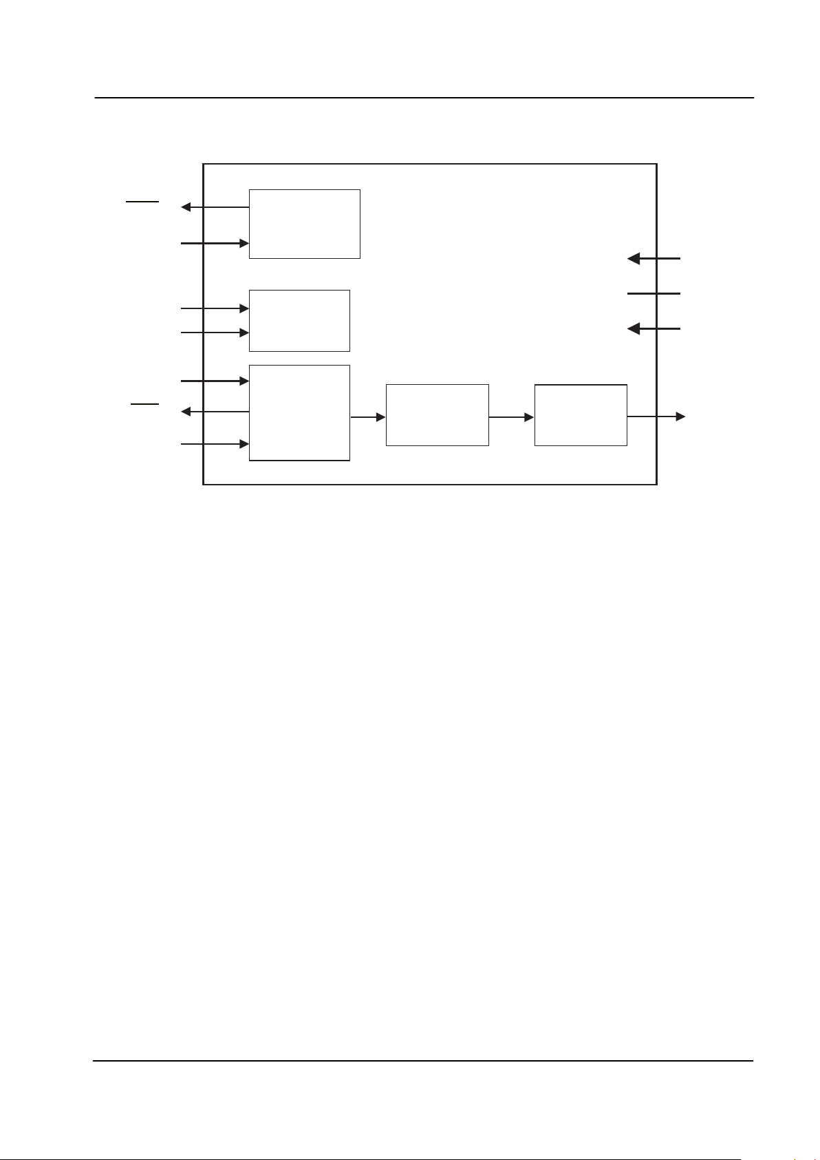
1 Block Diagram
TXD
M0
CLK
RDY
M1
Mode
Control
Logic
Tx Data
Re-timing
Transmit
Filter and
Output Buffer
FSK
Modulator
TXOUT
Xtal Osc and
Clock Dividers
XTAL/
CLOCK
XTAL
V
DD
V
BIAS
V
S
S
CMX654
Figure 1: Block Diagram
Page 4
V.23 Transmit Modulator 4 CMX654 PRELIMINARY INFORMATION
¤1998 MX-COM, Inc. www.mxcom.com Tel: 800 638 5577 336 744 5050 Fax: 336 744 5054 Doc. # 20480186.001
4800 Bethania Station Road, Winston-Salem, NC 27105-1201 USA All Trademarks and Service marks are held by their respective companies.
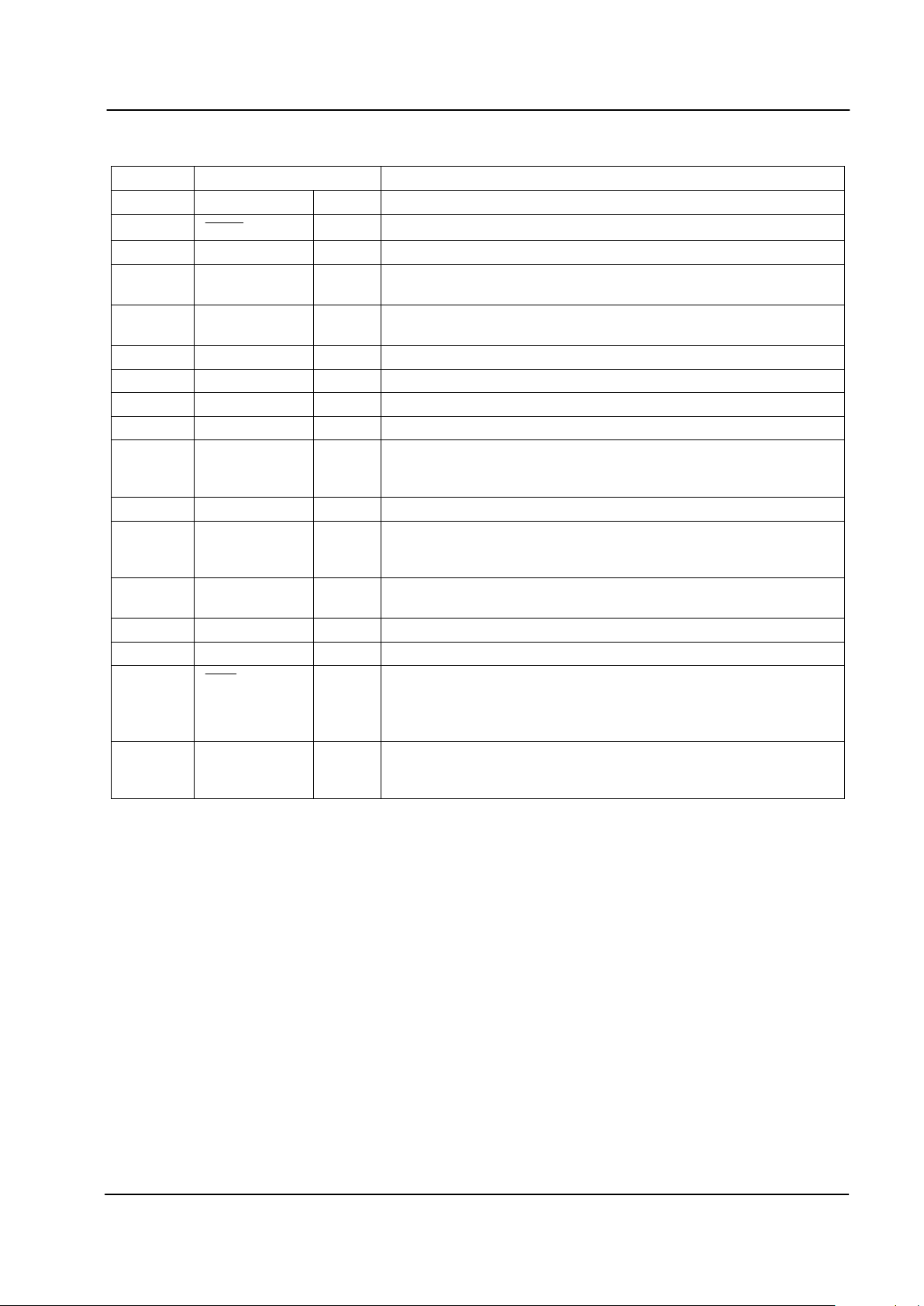
2 Signal List
D4/P3 Signal Description
Pin No. Name Type
1
XTAL
input The output of the on-chip Xtal oscillator inverter.
2 XTAL/CLOCK input The input to the on-chip Xtal oscillator inverter.
3 M0 input A logic level input for setting the mode of the device.
See Section 4.2.
4 M1 input A logic level input for setting the mode of the device.
See Section 4.2.
5 Connect to VSS.
6 N/C No connection, do not connect to this pin.
7 TXOUT output The output of the FSK generator.
8V
SS
Power The negative supply rail (ground).
9V
BIAS
output Internally generated bias voltage, held at VDD/2 when the device is
not in 'Zero-Power' mode. Should be decoupled to V
SS
by a
capacitor mounted close to the device pins.
10 - - Connect to V
DD
.
11 TXD input A logic level input for either the raw input to the FSK Modulator or
data to be re-timed depending on the state of the M0, M1 and CLK
inputs. See Section 4.3.
12 CLK input A logic level input which may be used to clock data bits into the Tx
FSK Data Retiming block.
13 - N/C No connection, do not connect to this pin.
14 - N/C No connection, do not connect to this pin.
15
RDY
output "Ready for Tx data transfer" output of the on-chip data retiming
circuit. This open-drain active low output may be used as an
Interrupt Request/Wake-up input to the associated PC. An external
pull-up resistor should be connected between this output and V
DD
.
16 V
DD
Power The positive supply rail. Levels and thresholds within the device
are proportional to this voltage. Should be decoupled to V
SS
by a
capacitor mounted close to the device pins.
VDD and V
BIAS
decoupling is very important. It is recommended that the decoupling capacitors be placed
so that connections between them and the device pins are as short as practicable.
Table 1: Signal List
Page 5

V.23 Transmit Modulator 5 CMX654 PRELIMINARY INFORMATION
¤1998 MX-COM, Inc. www.mxcom.com Tel: 800 638 5577 336 744 5050 Fax: 336 744 5054 Doc. # 20480186.001
4800 Bethania Station Road, Winston-Salem, NC 27105-1201 USA All Trademarks and Service marks are held by their respective companies.
3 External Components
V
DD
V
DD
V
BIAS
V
SS
CMX654
D4/P3
16
15
14
13
12
11
10
98
7
6
5
4
3
2
1
N/C
N/C
N/C
RDY
CLK
TXD
M1
TXOUT
M0
To/From µC
From µC
C1
C2
C3
C4
X1
R1
XTAL/CLOCK
XTAL
Figure 2: External Components
R1
100k
:
C1, C2 18pF
C3
0.1PF
C4
0.1PF
X1 Note 1 3.579545MHz
Resistors r5%, capacitors r10% unless otherwise stated
Table 2: External Components for Typical Application
External Components Notes:
1. A crystal frequency of 3.579545MHzr0.1% is required for correct FSK operation. For best results, a
crystal oscillator design should drive the clock inverter input with signal levels of at least 40% of V
DD
,
peak-peak. Tuning fork crystals generally cannot meet this requirement. To obtain crystal oscillator
design assistance, consult your crystal manufacturer. Operation of this device without a Xtal or Clock
input may cause device damage.
Page 6

V.23 Transmit Modulator 6 CMX654 PRELIMINARY INFORMATION
¤1998 MX-COM, Inc. www.mxcom.com Tel: 800 638 5577 336 744 5050 Fax: 336 744 5054 Doc. # 20480186.001
4800 Bethania Station Road, Winston-Salem, NC 27105-1201 USA All Trademarks and Service marks are held by their respective companies.
4 General Description
4.1 Xtal Oscillator and Clock Dividers
Frequency and timing accuracy of the CMX654 is determined by a 3.579545MHz clock present at the
XTAL/CLOCK pin. This may be generated by the on-chip oscillator inverter using the external components
C1, C2 and X1 of Figure 2, or may be supplied from an external source to the XTAL/CLOCK input. If supplied
from an external source, C1, C2 and X1 should not be fitted.
The on-chip oscillator is turned off in the 'Zero-Power' mode.
If the clock is provided by an external source, which is not always running, then the 'Zero-Power' mode must
be set when the clock is not available. Failure to observe this rule may cause a significant rise in the supply
current drawn by CMX654 as well as generating undefined states of the
RDY output.
4.2 Mode Control Logic
The CMX654's operating mode is determined by the logic levels applied to the M0 and M1 input pins:
M1 M0 Tx Mode Data Retime
[1]
0 1 1200bits/sec Tx
10 off 1 1 'Zero-Power' -
[1] If enabled
In the 'Zero-Power' mode, power is removed from all internal circuitry. When leaving 'Zero-Power' mode there
must be a delay of 20ms before any Tx data is passed to the device to allow the bias level, filters and
oscillator to stabilize. On applying power to the device the mode must be set to 'ZP', i.e. M0=1, M1=1, until
V
DD
has stabilized.
4.3 FSK Modulator and Transmit Filter
These blocks produce a tone according to the TXD, M0 and M1 inputs as shown in the table below, assuming
data retiming is not being used:
M1 M0 TXD = '0' TXD = '1'
1 1 ‘Zero Power’ ‘Zero Power’
10 0Hz 0Hz
[1]
0 1 2100Hz 1300Hz
[1] TXOUT held at approx. VDD/2.
When modulated at the appropriate baud rates, the Transmit Filter and associated external components (see
Section 5.1) limit the FSK out of band energy sent to the line in accordance with Figure 3 assuming that the
signal on the line is at -6dBm or less.
Page 7

V.23 Transmit Modulator 7 CMX654 PRELIMINARY INFORMATION
¤1998 MX-COM, Inc. www.mxcom.com Tel: 800 638 5577 336 744 5050 Fax: 336 744 5054 Doc. # 20480186.001
4800 Bethania Station Road, Winston-Salem, NC 27105-1201 USA All Trademarks and Service marks are held by their respective companies.
Figure 3: Tx Limits
4.4 Tx Data Retiming
The Data Retiming block, when enabled in 1200bits/sec transmit mode, requires the controlling PC to load 1
bit at a time into the device by a pulse applied to the CLK input. The timing of this pulse is not critical and it
may easily be generated by a simple software loop. This facility removes the need for a UART in the PC
without incurring an excessive software overhead.
The Tx re-timing circuit consists of two 1-bit registers in series, the input of the first is connected to the TXD
pin and the output of the second feeds the FSK modulator. The second register is clocked by an internally
generated 1200Hz signal and when this occurs the CLK input is sampled. If the CLK input is high the TXD pin
directly controls the FSK modulator, if the CLK input is low the FSK modulator is controlled by the output of
the second register and the
RDY pin is pulled low. The RDY output is reset by a high level on the CLK input
pin. A low to high change on the CLK input pin will latch the data from the TXD input pin into the first register
ready for transfer to the second register when the internal 1200Hz signal next occurs.
So to use the retiming option the CLK input should be held low until the
RDY output is pulled low. When the
RDY pin goes low the next data bit should be applied at the TXD input and the CLK input pulled high and then
low within the time limits set out in Figure 7.
To ensure synchronization between the controlling device and the CMX654 when entering Tx retiming mode,
the TXD pin must be held at a constant logic level from when the CLK pin is first pulled low to the end of
loading in the second retimed bit. Similarly when exiting Tx retiming mode the TXD pin should be held at the
same logic level as the last retimed bit for at least 2 bit times after the CLK line is pulled high.
If the data retiming facility is not required, the CLK input to the CMX654 should be kept high at all times. The
asynchronous data to the FSK modulator will then be connected directly to the TXD input pin. This is
illustrated in Figure 4.
N-2
N-2
N-1
N-1NN
N+1
N+1
N+2
N+2
FSK Modulator input:
TXD input:
Figure 4: FSK Operation without Tx Data Retiming (CLK always high)
Page 8

V.23 Transmit Modulator 8 CMX654 PRELIMINARY INFORMATION
¤1998 MX-COM, Inc. www.mxcom.com Tel: 800 638 5577 336 744 5050 Fax: 336 744 5054 Doc. # 20480186.001
4800 Bethania Station Road, Winston-Salem, NC 27105-1201 USA All Trademarks and Service marks are held by their respective companies.
5 Application Notes
5.1 Line Interface
The signals on the telephone line are not suitable for direct connection to the CMX654. A Line Interface
circuit is necessary to:
x
Provide high voltage and DC isolation
x
Provide the low impedance drive necessary for the line
x
Filter the Tx and Rx signals
LINE
1:1
R3
R6
Z
TXOUT
POSSIBLE
RECEIVE - HYBRID
CIRCUITRY
V
BIAS
A
B
C
A1
0V
C5
C7
+
Figure 5: Line Interface Circuit
R3 Note 3 C5
22PF (r20%)
R6
100k
:
C7 330pF
Resistors r1%, capacitors r10% unless otherwise stated.
Notes:
1. The component(s) 'Z' between points B and C should match the line impedance.
2. Device A1 must be able to drive 'Z' and the line.
3. R3: The levels in dB (relative to a 775mV
RMS
signal) at 'A', 'B' and 'C' in the line interface circuit are:
‘A' = 20Log(V
DD
/5)
'B' = 'A' + 20Log(100k:/R3)
'C' = 'B' - 6
V
DD
'A' R3 'B' 'C'
3.3V -3.6dB
100k
:
-3.6dB -9.6dB
5.0V 0dB
150k
:
-3.5dB -9.5dB
Page 9

V.23 Transmit Modulator 9 CMX654 PRELIMINARY INFORMATION
¤1998 MX-COM, Inc. www.mxcom.com Tel: 800 638 5577 336 744 5050 Fax: 336 744 5054 Doc. # 20480186.001
4800 Bethania Station Road, Winston-Salem, NC 27105-1201 USA All Trademarks and Service marks are held by their respective companies.
6 Performance Specification
6.1 Electrical Performance
6.1.1 Absolute Maximum Ratings
Exceeding these maximum ratings can result in damage to the device.
Min. Max. Units
Supply (VDD - VSS) -0.3 7.0 V
Voltage on any pin to V
SS
-0.3 V
DD
+ 0.3 V
Current into or out of:
V
DD
-30 30 mA
V
SS
-30 30 mA
Any other pin -20 20 mA
D4 / P3 Package
Total Allowable Power Dissipation at T
AMB
= 25°C 800 mW
Derating above 25°C 13 mW/°C above 25°C
Storage Temperature -55 125 °C
Operating Temperature -40 85 °C
6.1.2 Operating Limits
Correct operation of the device outside these limits is not implied.
Notes Min. Max. Units
Supply (VDD - VSS)3.05.5V
Operating Temperature -40 85 °C
Xtal Frequency 1 3.575965 3.583125 MHz
Notes:
1. A Xtal frequency of 3.579545MHz ±0.1% is required for correct FSK operation.
Page 10

V.23 Transmit Modulator 10 CMX654 PRELIMINARY INFORMATION
¤1998 MX-COM, Inc. www.mxcom.com Tel: 800 638 5577 336 744 5050 Fax: 336 744 5054 Doc. # 20480186.001
4800 Bethania Station Road, Winston-Salem, NC 27105-1201 USA All Trademarks and Service marks are held by their respective companies.
6.1.3 Operating Characteristics
For the following conditions unless otherwise specified:
V
DD
= 3.0V at T
AMB
= 25°C and V
DD
= 3.3V to 5.5V at T
AMB
= -40 to +85°C,
Xtal Frequency = 3.579545MHz r 0.1%, 0dBV corresponds to 1.0V
RMS
,
0dBm corresponds to 775mV
RMS
into 600:.
Notes Min. Typ. Max. Units
DC Parameters
IDD (M0='1', M1='1') 1, 2 1
P
A
IDD (M0 or M1='0') at VDD = 3.0V 1 1.0 1.25 mA
IDD (M0 or M1='0') at VDD= 5.0V 1 1.7 2.5 mA
Logic '1' Input Level 70% V
DD
Logic '0' Input Level 30% V
DD
Logic Input Leakage Current (VIN = 0 to VDD), Excluding
XTAL/CLOCK Input
-1.0 1.0
P
A
Output Logic '1' Level (lOH = 360PA)
V
DD
-0.4 V
Output Logic '0' Level (l
OL
= -360PA)
0.4 V
RDY Output 'off' State Current (V
OUT
= VDD)
1.0
P
A
FSK Retiming
Tx Data Rate 1194 1206 Baud
FSK Modulator
TXOUT Level 3 -1.0 0 1.0 dB
Twist (Mark Level WRT Space Level) -2.0 0 2.0 dB
Tx 1200bits/sec (M1='0', M0='1').
Bit Rate 0 1200 1212 Baud
Mark (Logical 1) Frequency 1297 1303 Hz
Space (Logical 0) Frequency 2097 2103 Hz
XTAL/CLOCK Input
'High' Pulse Width 4 100 ns
'Low' Pulse Width 4 100 ns
Operating Characteristics Notes:
1. At 25
qC, not including any current drawn from the CMX654 pins by external circuitry other than X1, C1
and C2.
2. TXD and CLK inputs at V
SS
, M0 and M1 inputs at VDD.
3. Relative to 775mV
RMS
at VDD= 5.0V for load resistance greater than 40k:.
4. Timing for an external input to the XTAL/CLOCK pin.
Page 11

V.23 Transmit Modulator 11 CMX654 PRELIMINARY INFORMATION
¤1998 MX-COM, Inc. www.mxcom.com Tel: 800 638 5577 336 744 5050 Fax: 336 744 5054 Doc. # 20480186.001
4800 Bethania Station Road, Winston-Salem, NC 27105-1201 USA All Trademarks and Service marks are held by their respective companies.
6.2 Timing
Data and Mode Timing Min. Typ. Max. Units
Delay to reliable data at TXOUT after ZP to Tx mode change 20.0 ms
Data Retiming Disabled (reference Figure 6)
Tx Data Delay (TXD to TXOUT) 0.1 ms
Data Retiming Enabled (reference Figure 7)
tD = Internal CMX654 delay 1
P
s
tcHI = CLK High time 1
P
s
tR = RDY low to CLK going low 800
P
s
tS = Data Set-up time 1
P
s
tH = Data Hold time 1
P
s
TXD
TXOUT (FSK Signal)
Tx Data D e lay
F
HI
F
LO
F
LO
F
HI
Note: M0 and M1 are preset and stable. F
LO
and FHI are the two FSK signaling frequencies.
Figure 6: TXD to TXOUT Delay time
1
1
1
2
3
4
32
FSK Modulator input
RDY
CLK
TXD
t
S
t
H
t
D
t
R
tc
HI
RDY
CLK
TXD
Figure 7: FSK Operation with Tx Data Retiming
Page 12

V.23 Transmit Modulator 12 CMX654 PRELIMINARY INFORMATION
¤1998 MX-COM, Inc. www.mxcom.com Tel: 800 638 5577 336 744 5050 Fax: 336 744 5054 Doc. # 20480186.001
4800 Bethania Station Road, Winston-Salem, NC 27105-1201 USA All Trademarks and Service marks are held by their respective companies.
6.3 Packaging
PIN 1
A
B
ALTERNATIVE
PIN
LOCATION
MARKING
X
P
J
Y
C
K
H
E
L
T
W
Z
NOTE: All dimensions in inches (mm.)
Angles are in degrees
PackageTolerances
A
B
C
E
H
TYP.
MAX.MIN.
DIM.
J
P
X
W
T
Y
K
L
0.105 (2.67)0.093 (2.36)
0.419 (10.64)
45°
7°
0° 10°
0.050 (1.27)
0.041 (1.04)
0.413 (10.49)
0.299 (7.59)
0.050 (1.27)
0.016 (0.41)
0.390 (9.90)
0.020 (0.51)0.003 (0.08)
0.009 (0.23) 0.0125 (0.32)
0.013 (0.33) 0.020 (0.51)
0.395 (10.03)
0.286 (7.26)
Z
5°
5°
Figure 8: 16-pin SOIC (D4) Mechanical Outline:
Order as part no. CMX654D4
PackageTolerances
NOTE: All dimensions in inches (mm.)
Angles are in degrees
TYP. MAX.MIN.
A
B
C
E
E1
H
DIM.
J
J1
P
Y
T
K
L
0.200 (5.06)
0.262 (6.63)
0.390 (9.91).
7°
0.150 (3.81)
0.810 (20.57)
0.135 (3.43)
0.100 (2.54)
0.121 (3.07)
0.300 (7.62)
0.290 (7.37) 0.325 (8.26)
0.015 (0.38) 0.070 (1.77)
0.008 (0.20) 0.015 (0.38)
0.014 (0.35) 0.023 (0.58)
0.040 (1.02) 0.065 (1.65)
0.056 (1.42) 0.064 (1.63)
0.740 (18.80)
0.240 (6.10)
B
A
PIN 1
E
Y
E1
T
K
H
J1
J
C
P
L
Figure 9: 16-pin PDIP (P3) Mechanical Outline:
Order as part no. CMX654P3
 Loading...